

Page 1

DATA SHEET
BIPOLAR ANALOG INTEGRATED CI RCUIT
µµµµ
PC3211GR
AGC AMPLIFIER FOR DIGITAL CATV RETURN PASS
DESCRIPTION
The µPC3211GR is a silicon monolithic integrated circuit designed as AGC amplifier for digital CATV systems. This
IC is the AGC amplifier with 55 dB gain control range which is packaged in 20-pin SSOP. The device is able to use
for digital QPSK system, therefore it contributes to make design of transmission system simplicity.
FEATURES
• Wide gain control range 55 dB TYP.
• Low distortion IM3 = 57 dBc TYP. @P
IM2 = 44 dBc TYP. @P
• Supply Voltage 9 V
• Packaged in 20-pin SSOP suitable for high-density surface mount.
out
= −10 dBm
out
= −10 dBm
ORDERING INFORMATION
Part Number Package Supplying Form
µ
PC3211GR-E1 20-pin plastic SSOP (225 m i l ) Embossed tape 12 mm wide.
Pin 1 indicates pull-out di rection of tape.
Qty 2.5 kp/reel
To order evaluation samples, please contact your local NEC office. (Part number for sample order: µPC3211GR)
The information in this document is subject to change without notice. Before using this document, please
confirm that this is the latest version.
Not all devices/types available in every country. Please check with local NEC representative for
availability and additional information.
Document No. P13564EJ3V0DS00 (3rd edition)
Date Published October 1999 N CP(K)
Printed in Japan
Caution electro-static sensitive device
The mark shows major revised points.
©
1998, 1999
Page 2
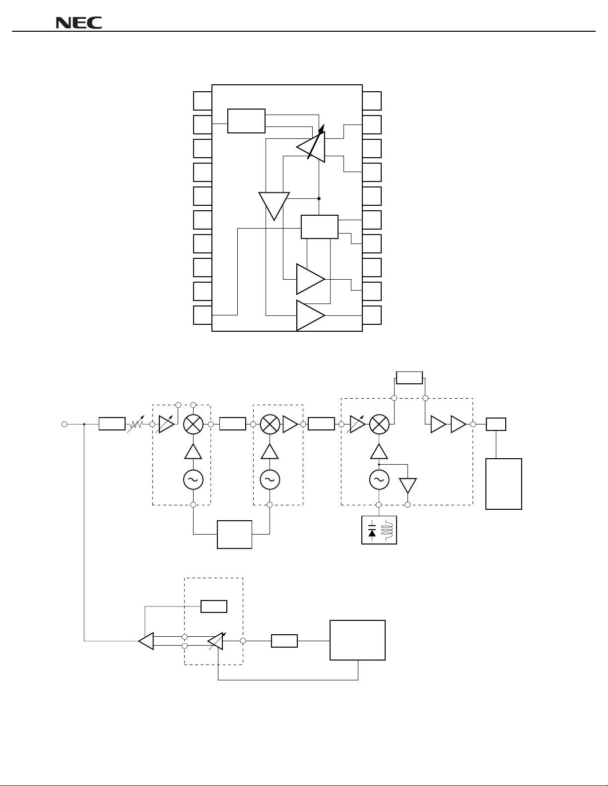
INTERNAL BLOCK DIAGRAM AND PIN CONFIGURATION (TOP VIEW)
BY1
BY2
1
20
µµµµ
PC3211GR
TYPICAL APPLICATION
RF IN
50-750 MHz
RF Return
5-42 MHz
HPF SAW SAW
VAGC
GND2A
GND2B
CC1
V
CC2
V
GND2C
GND2D
GND2E
BY3
PC2799GR
µ
10
2
Cont.
3
4
5
6
REG
7
8
9
PC2798GR
µ
1st IF
PC1686GV
µ
2nd IF
19
18
17
16
15
14
13
12
11
AGC IN1
GND1A
AGC IN2
GND1B
PSAVE
PA_BIAS
GND3
OUT1
OUT2
LPF
DC-10 MHz
A/D
Video Amplifier
QAM
Demo.
&FEC
DUAL
PLL
PC3211GR
µ
Bias
Digital
LPF
2
Data Sheet P13564EJ3V0DS00
QPSK
Modulator
Page 3
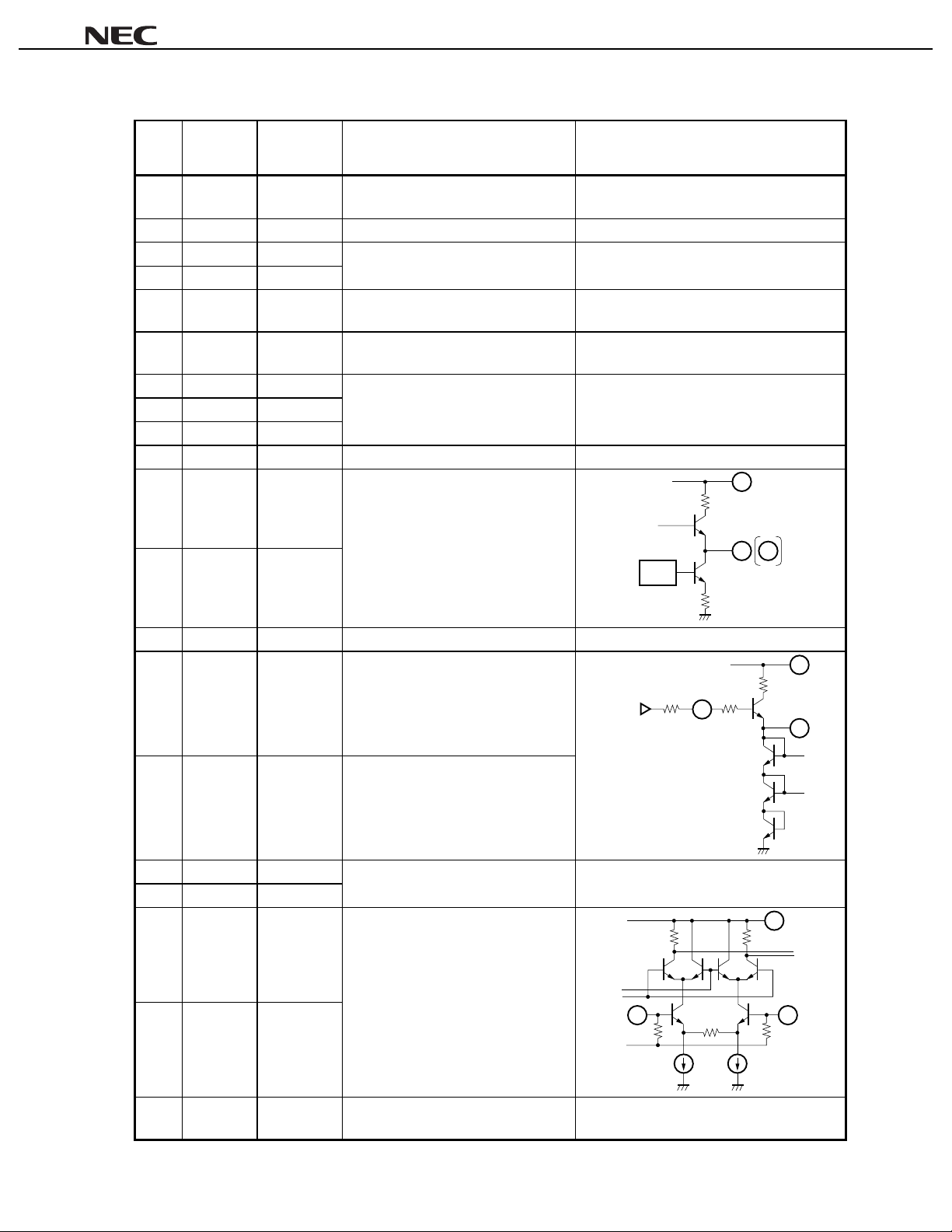
PIN FUNCTIONS
µµµµ
PC3211GR
Pin
No.
Pin
Name
Pin
Voltage
TYP. (V)
Function and Explanation Equivalent Circuit
1 BY2 – Non Connection pin.
This pin should be opened.
2 VAGC 0 to 3 Automatic gain control pi n.
3 GND2A 0.0
Ground pins of differential ampl i fier.
4 GND2B 0.0
5V
cc
1 9.0 Power supply pin of AGC ampli f i er
block.
6V
cc
2 9.0 Power supply pin of differential
amplifier and output block .
7 GND2C 0.0
Ground pins of differential ampl i fier.
8 GND2D 0.0
9 GND2E 0.0
10 BY3 1.64 Bypass pi n of regulator block.
11 OUT2 6.9
Signal output pins.
This pins feature low-impedanc e
because of its emitter-follower output
port.
12 OUT1 6.9
The pin that is not used should be
grounded through 50 ohm resistor.
6
11 12
REG
13 GND3 0.0 Ground pin of output block.
14 PA_BIAS 2.45 This is the pin to feed base bias i n
case of connection to transistor as
power amplifier.
15 Psave 9.0
(+5 kΩ)
Power-save pin.
cc
:ON
V
GND : SLEEP
The 5 kΩ resistor should be
connected between 15 pin and V
16 GND1B 0.0
Ground pin of AGC amplifier block.
18 GND1A 0.0
17 AGC IN2 2.43
Signal input pin.
In the case of single input, 17 or 19
pin should be grounded through
capacitor.
19 AGC IN1 2.43
5
V
CC
(9 V)
cc
.
5 kΩ
15
14
5
1719
20 BY1 – Non Connection pin.
This pin should be opened.
Data Sheet P13564EJ3V0DS00
3
Page 4
ABSOLUTE MAXIMUM RATINGS (TA = +25°C unless otherwise specified)
Parameter Symbol Test Condition Rating Unit
µµµµ
PC3211GR
Supply Voltage V
Power-save Voltage V (Psave)
AGC Voltage V
Power Dissipation P
Operating Ambient Temperature T
Storage Temperature T
CC
AGC
stg
D
A
TA = +75°C
Note 1
Note 2
11.0 V
11.0 V
3.6 V
500 mW
40 to +75 °C
−
55 to +150 °C
−
Maximum Input Level Pin (MAX) +5 dBm
Notes 1.
Bias to 15 pin through 5 kΩ resistor.
Mounted on 50 mm × 50 mm × 1.6 mm double epoxy glass board.
2.
RECOMMENDED OPERATING RANGE
Parameter Symbol Test Condition MIN. TYP. MAX. Unit
Supply Voltage V
Power-save Voltage V (Psave)
AGC Control Voltage V
Operating Ambient Temperature T
Input Frequency f
Maximum Input Level Pin (MAX) – – 0 dBm
CC
AGC
in
8.0 9.0 10.0 V
Note
0 – 10.0 V
0–3.3V
A
40 +25 +75 °C
−
5 – 100 MHz
Bias to 15 pin through 5 kΩ resistor.
Note
ELECTRICAL CHARACTERISTICS (TA = +25°C, VCC = 9 V, V
AGC
= 0 V, V (Psave) = 9 V (+5 k
specified)
Parameter Symbol Test Conditions MIN. TYP. MAX. Unit
Circuit Current 1 ICC1
Maximum Gain G
MAX
Gain Control Range GCR fin = 65 MHz, Pin = −20 dBm,
Isolation at sleep mode Isol fin = 65 MHz, Pin = −20 dBm,
2nd
order intermodulation distorti on IM
3rd order intermodulation distorti on IM
Notes 1.
By measurement circuit 1
By measurement circuit 2
2.
No input signal
fin = 65 MHz, Pin = −20 dBm
AGC
= 0 to 3 V
V
V (Psave) = 0 V (+5 kΩ)
2
fin1 = 65 MHz, fin2 = 66.8 MHz,
out
= −10 dBm
P
3
fin1 = 65 MHz, fin2 = 66.8 MHz,
out
= −10 dBm
P
Note 1
Note 2
Note 2
Note 2
Note 2
Note 2
), unless otherwise
ΩΩΩΩ
29 38 51 mA
14 16 18 dB
47 55 – dB
60 65 – dB
– –44 –40 dBc
– –57 –50 dBc
4
Data Sheet P13564EJ3V0DS00
Page 5
µµµµ
PC3211GR
in
= 65 MHz
in
= −20 dBm
AGC
= 0 V, V (Psave) = 9 V (+5 k
AGC
= 3 V
STANDARD CHARACTERISTICS (TA = +25°C, VCC = 9 V, V
Parameter Symbol Test Conditions Reference Value Unit
Maximum Output Power P
Circuit Current at Power-save mode ICC (P/S) No input signal, V (Psave) = 0 V (+5 kΩ)
Noise Figure NF
Output Intercept Point OIP
Gain Flatness G
Circuit Current 2 ICC2
ON Time t
OFF Time t
Notes 1.
By measurement circuit 2
By measurement circuit 1
2.
By measurement circuit 3
3.
By measurement circuit 4
4.
O (sat)
ON
OFF
fin = 65 MHz, Pin = −5 dBm
f
fin1 = 65 MHz, fin2 = 66.8 MHz
3
flat
fin = 5 to 100 MHz, 6 MHz Band width
P
No input signal, V
fin = 65 MHz,
V (Psave) = 0 → 9 V (+5 kΩ)
fin = 65 MHz,
V (Psave) = 9 → 0 V (+5 kΩ)
Note 1
Note 2
Note 3
Note 1
Note 1
Note 2
Note 4
Note 4
), unless otherwise specified)
ΩΩΩΩ
+5 dBm
3mA
10 dB
+16 dBm
±0.1 dB
43 mA
200
1.7 msec
µ
sec
Data Sheet P13564EJ3V0DS00
5
Page 6

TYPICAL CHARACTERISTICS (TA = +25°C)
µµµµ
PC3211GR
CIRCUIT CURRENT vs. SUPPLY VOLTAGE
50
40
(mA)
30
CC
20
Circuit Current I
10
no input signal
measurement
0
246
0
circuit1
81012
Supply Voltage VCC (V)
Power-sa ve Voltage V(Psav e) (V)
CIRCUIT CURRENT vs. AGC VOLTAGE
45
44
43
42
(mA)
41
CC
40
39
38
Circuit Current I
37
36
35
0 0.5 1 1.5
AGC V oltage V
no input signal
CC
V
V(Psave) = 9V
measurement
circuit1
2 2.5 3 3.5
AGC
(V)
= 9 V
CIRCUIT CURRENT vs. POWER-SAVE VOLTAGE
40
35
30
(mA)
25
CC
20
15
Circuit Current I
10
5
0
0
246
no input signal
V
measurement
circuit1
81012
Power-sa ve Voltage V(Psave) (V)
14PIN VOLTAGE vs. SUPPLY VOLTAGE
3
2.5
2
1.5
1
14 pin Voltage V(14) (V)
0.5
no input signal
V
measurement
0
246
0
circuit1
81012
Supply Voltage VCC (V)
Power-sa ve Voltage V(Psave) (V)
CC
AGC
= 9 V
= 0 V
20
GAIN vs. INPUT FREQUENCY
−20
GAIN vs. INPUT FREQUENCY
Pin = −20 dBm
V
AGC
= 3 V
measurement
18
−30
circuit2
16
−40
Gain (dB)
14
Gain (dB)
VCC = V(Psave)
= 8 to 10 V
12
in
= −20 dBm
P
V
AGC
= 0 V
measurement
circuit2
10
02040
Input Frequency f
6
60 80 100
in
(MHz)
Data Sheet P13564EJ3V0DS00
−50
−60
02040
Input Frequency f
Vcc = V(Psave) = 8 V
Vcc = V(Psave) = 9 V
Vcc = V(Psave) = 10 V
60 80 100
in
(MHz)
Page 7

µµµµ
PC3211GR
20
GAIN vs. AGC VOLTAGE
10
0
−10
−20
Gain (dB)
−30
−40
VCC = V(Psave) = 8 V
VCC = V(Psave) = 9 V
−50
VCC = V(Psave) = 10 V
0 0.5 1 1.5
2 2.5 3.53
AGC V oltage V
OUTPUT POWER vs. INPUT POWER
20
0
V
AGC
= 0 V
V
AGC
(dBm)
−20
out
= 1.1 V
−40
V
AGC
= 2.2 V
Output Power P
−60
−80
−30 −25 −20 −15
V
AGC
= 3 V
Input Power P
fin = 65 MHz
in
= −20 dBm
P
measurement
circuit2
AGC
(V)
V
AGC
= 1.5 V
VCC = 9 V
V(Psave) = 9 V
f
in
= 65 MHz
measurement
circuit2
−10 −50
in
(dBm)
OUTPUT POWER vs. INPUT POWER
10
fin = 65 MHz
AGC
= 0 V
V
measurement
5
circuit2
0
(dBm)
out
−5
−10
Output Power P
−15
VCC = V(Psave) = 8 V
VCC = V(Psave) = 9 V
−20
−30 −25 −20 −15
Input Power P
NOISE FIGURE vs. INPUT FREQUENCY
12
V
AGC
= 0 V
VCC = V(Psave) = 10 V
−10 −50
in
(dBm)
measurement
circuit3
11
10
Noise Figure NF (dB)
9
VCC = V(Psave) = 8 V
CC
= V(Psave) = 9 V
V
V
CC
8
02040
Input Frequency f
= V(Psave) = 10 V
60 80 100
in
(MHz)
30
GAIN vs. INPUT FREQUENCY
20
10
0
−10
−20
−30
Gain (dB)
−40
−50
−60
−70
−80
02040
Input Frequency f
V
AGC
= 0 V
V
AGC
= 1.1 V
V
AGC
= 1.5 V
V
AGC
= 2.2 V
V
AGC
= 3 V
V
AGC
= 3.3 V
VCC = 9 V
V(Psave) = 9 V
in
= −20 dBm
P
measurement
circuit2
60 80 100
in
(MHz)
Data Sheet P13564EJ3V0DS00
7
Page 8

STANDARD CHARACTERISTICS (TA = +25°C)
µµµµ
PC3211GR
3rd ORDER INTERMODULATION DISTORTION
20
10
0
−10
−20
/ tone (dBm)
out
−30
−40
−50
−60
Output Power P
−70
−80
−40 −30 −20 −10
Input Power P
−10
(dBc)
3
−20
−30
IM3 vs. OUTPUT POWER
VCC = V(Psave) = 9 V
f
in
1 = 65 MHz
in
2 = 66.8 MHz
f
V
AGC
= 0 V
out
= −13 dBm/tone
P
= −
10 dBm(total)
measurement
VCC = V(Psave) = 9 V
in
1 = 65 MHz
f
in
2 = 66.8 MHz
f
AGC
= 0 V
V
out
P
= −13 dBm/tone
= −10 dBm(total)
measurement circuit2
in (dBm)
circuit2
−40
2nd ORDER INTERMODULATION DISTORTION
20
10
0
−10
−20
/ tone (dBm)
out
−30
−40
−50
−60
Output Power P
−70
−80
−40 −30 −20 −10
Input Power P
0
(dBc)
2
−10
−20
IM2 vs. OUTPUT POWER
VCC = V(Psave) = 9 V
in
1 = 65 MHz
f
in
2 = 66.8 MHz
f
AGC
= 0 V
V
P
out
= −13 dBm/tone
= −10 dBm(total)
measurement
VCC = V(Psave) = 9 V
f
in1 = 65 MHz
f
in2 = 66.8 MHz
V
AGC = 0 V
P
out = −13 dBm/tone
= −10 dBm(total)
measurement circuit2
in (dBm)
circuit2
−30
−50
−60
3rd Order Intermodulation Distortion IM
−70
−20
−15 0−10
Output Power Pout/tone (dBm)
ON/OFF TIME OF POWERSAVE
REF 0.0 dBm
10 dB/
RBW
3 MHz
VBW
3 MHz
SWP
7.5 ms
CENTER 65.000000 MHz SPAN 0 Hz
ATT 10 dB
VCC = 9 V
in
f
P
Input Voltage = 9 V
measurement
circuit4
−5
= 65 MHz
in
= −20 dBm
−40
−50
2nd Order Intermodulation Distortion IM
−60
−20
−15 0−10
−5
Output Power Pout/tone (dBm)
8
Data Sheet P13564EJ3V0DS00
Page 9

THERMAL CHARACTERISTICS (FOR REFERENCE)
µµµµ
PC3211GR
CIRCUIT CURRENT vs. AMBIENT TEMPERATURE
50
V
AGC
= 3 V
40
V
AGC
(mA)
30
CC
= 0 V
20
Circuit Current I
10
no input signal
CC
= 9 V
V
V(Psave) = 9 V
measurement
0
circuit1
−50 −25 0 25 50 75 100
A
(°C)
20
Ambient T emperature T
GAIN vs. AGC VOLTAGE
VCC = 9 V
10
0
V(Psave) = 9 V
f
in
= 65 MHz
P
in
= −20 dBm
measurement
circuit2
20
GAIN vs. INPUT FREQUENCY
TA = −40 °C
T
18
T
16
14
Gain (dB)
VCC = 9 V
V(Psave) = 9 V
in
= −20 dBm
P
12
AGC
= 0 V
V
measurement
circuit2
10
0 20 40 60 80 100
Input Frequency f
in
(MHz)
A
= +25 °C
A
= +75 °C
−10
−20
Gain (dB)
−30
−40
−50
TA = −40 °C
A
= +25 °C
T
A
= +75 °C
T
0 0.5 1.51 2 2.5 3 3.5
AGC
AGC V oltage V
(V)
Data Sheet P13564EJ3V0DS00
9
Page 10

STANDARD CHARACTERISTICS
INPUT IMPEDANCE (19 PIN)
S
11
1 U FS
hp
3
START .100 000 MHz STOP 100.000 000 MHz
1: 5 MHz
∆
533.6
Ω
16.4
−
Ω
2: 40 MHz
∆
515.2
Ω
81.4
−
Ω
3: 65 MHz
∆
493.7
Ω
123.3
−
Ω
4: 100 MHz
∆
455.9
Ω
190.3
−
Ω
TA = +25°C
VCC = 9 V
V (Psave) = 9 V
Pin = −20 dBm
µµµµ
PC3211GR
OUTPUT IMPEDANCE (11 PIN)
S
22
1 U FS
hp
3
4
2
1
START 5.000 000 MHz STOP 100.000 000 MHz
1: 5 MHz
∆
9.779
Ω
2.306
−
Ω
2: 40 MHz
∆
10.066
Ω
3.033
Ω
3: 65 MHz
∆
10.574
Ω
5.237
Ω
4: 100 MHz
∆
11.88
Ω
7.805
Ω
TA = +25°C
VCC = 9 V
V (Psave) = 9 V
Pin = −20 dBm
10
Data Sheet P13564EJ3V0DS00
Page 11

MEASUREMENT CIRCUIT 1
µµµµ
PC3211GR
V
AGC
V
CC
The pin that is not connected to Spectrum Analyzer should be grounded through 50 Ω resistor.
Note
100 pF
100 pF
0.01 F
µ
0.1 F
MEASUREMENT CIRCUIT 2
0.01 F
µ
µ
10
1
2
3
4
5
6
7
8
9
Cont.
REG
20
19
18
17
16
15
14
13
12
11
0.1 F
0.1 F
100 pF
10 kΩ
0.1 F
0.1 F
µ
µ
5 kΩ 0.01 F
µ
µ
µ
AGC IN
V(Psave)
AGC OUT
AGC OUT
Note
Note 1
SG1
(50 Ω)
1
0.01 F
0.1 F
µ
µ
2
3
4
5
6
7
8
9
10
AGC
V
V
CC
100 pF
100 pF
0.01 F
µ
Cont.
REG
20
19
18
17
16
15
14
13
12
11
0.1 F
0.1 F
100 pF
10 kΩ
0.1 F
0.1 F
µ
µ
5 kΩ 0.01 F
µ
µ
µ
Note 2
MIXPAD
SG2
(50 Ω)
V(Psave)
Spectrum
Analyzer
(50 Ω)
Notes 1.
2
3
Connect in the case of measurement of IM
The pin that is not connected to Spectrum Analyzer should be grounded through 50 Ω resistor.
2.
Data Sheet P13564EJ3V0DS00
/IM
11
Page 12

MEASUREMENT CIRCUIT 3
µµµµ
PC3211GR
V
AGC
V
CC
Note
100 pF
0.01 F
100 pF
The pin that is not connected to Spectrum Analyzer should be grounded through 50 Ω resistor.
0.01 F
µ
0.1 F
MEASUREMENT CIRCUIT 4
1
µ
2
3
4
5
6
7
8
9
10
Cont.
REG
20
19
18
17
16
15
14
13
12
11
0.1 F
0.1 F
100 pF
10 kΩ
0.1 F
0.1 F
µ
µ
5 kΩ 0.01 F
µ
µ
µ
Noise
Source
NF
METER
V(Psave)
Note
µ
1
µ
AGC
V
V
CC
100 pF
0.01 F
100 pF
0.01 F
µ
0.1 F
2
3
4
5
6
7
8
9
10
µ
Cont.
REG
20
19
18
17
16
15
14
13
12
11
0.1 F
0.1 F
5 kΩ 0.01 F
100 pF
10 kΩ
0.1 F
0.1 F
µ
SG1
(50 Ω)
µ
µ
Pulse
Generator
(9 V, 2.3 msec)
Spectrum
µ
µ
Analyzer
(50 Ω)
50 Ω
12
Data Sheet P13564EJ3V0DS00
Page 13

ILLUSTRATION OF THE EVALUATION BOARD FOR MEASUREMENT CIRCUIT
V(Psave)
AGC IN1 OUT 1
µµµµ
PC3211GR
0.1
100 p
µ
0.1
0.01
µ
100 p
µ
5 k
0.01
µ
10 k
100 p
0.01
PC3211GR
µ
0.1
µ
0.1
µ
OUT 2
0.1
µ
µ
Notes 1.
V
AGC
CC
V
50 × 50 × 1.6 mm double sided copper clad polyimide board.
Back side: GND pattern
2.
Solder plated on pattern
3.
: Through holes
4.
Data Sheet P13564EJ3V0DS00
13
Page 14

PACKAGE DIMENSIONS
20 PIN PLASTIC SSOP (225 mil) (UNIT: mm)
µµµµ
PC3211GR
20
110
6.7 ± 0.3
1.8 MAX.
1.5 ± 0.1
11
detail of lead end
3˚
6.4 ± 0.2
4.4 ± 0.1
+7˚
–3˚
1.0 ± 0.2
NOTE
0.5 ± 0.2
0.15
+0.10
–0.05
0.1 ± 0.1
0.65
0.22
+0.10
–0.05
0.10
0.15
M
0.575 MAX.
Each lead centerline is located within 0.10 mm of its true position (T.P.) at maximum material condition.
14
Data Sheet P13564EJ3V0DS00
Page 15

µµµµ
PC3211GR
RECOMMENDED SOLDERING CONDITIONS
This product should be soldered under the following recommended conditions. For soldering methods and
conditions other than those recommended below, contact your NEC sales representative.
Soldering Method Soldering Conditions
Infrared Reflow Package peak temperature: 235°C or below
Time: 30 seconds or less (at 210°C)
Count: 3, Exposure limi t
VPS Package peak temperature: 215° C or bel ow
Time: 40 seconds or less (at 200°C)
Count: 3, Exposure limi t
Partial Heating Pin temperature: 300°C
Time: 3 seconds or less (per side of device)
Exposure limit
After opening the dry pack, keep it in a place below 25°C and 65% RH for the allowable storage period.
Note
Note
: None
Note
Note
: None
: None
Recommended Condition
Symbol
IR35-00-3
VP15-00-3
–
Caution Do not use different soldering methods together (except for partial heating).
For details of the recommended soldering conditions for surface mounting, refer to infor mation document
SEMICONDUCTOR DEVICE MOUNTING TECHNOLOGY MANUAL (C10535E)
.
Data Sheet P13564EJ3V0DS00
15
Page 16

µµµµ
PC3211GR
• The information in this document is subject to change without notice. Before using this document, please
confirm that this is the latest version.
• No part of this document may be copied or reproduced in any form or by any means without the prior written
consent of NEC Corporation. NEC Corporation assumes no responsibility for any errors which may appear in
this document.
• NEC Corporation does not assume any liability for infringement of patents, copyrights or other intellectual property
rights of third parties by or arising from use of a device described herein or any other liability arising from use
of such device. No license, either express, implied or otherwise, is granted under any patents, copyrights or other
intellectual property rights of NEC Corporation or others.
• Descriptions of circuits, software, and other related information in this document are provided for illustrative
purposes in semiconductor product operation and application examples. The incorporation of these circuits,
software, and information in the design of the customer's equipment shall be done under the full responsibility
of the customer. NEC Corporation assumes no responsibility for any losses incurred by the customer or third
parties arising from the use of these circuits, software, and information.
• While NEC Corporation has been making continuous effort to enhance the reliability of its semiconductor devices,
the possibility of defects cannot be eliminated entirely. To minimize risks of damage or injury to persons or
property arising from a defect in an NEC semiconductor device, customers must incorporate sufficient safety
measures in its design, such as redundancy, fire-containment, and anti-failure features.
• NEC devices are classified into the following three quality grades:
"Standard", "Special", and "Specific". The Specific quality grade applies only to devices developed based on a
customer designated "quality assurance program" for a specific application. The recommended applications of
a device depend on its quality grade, as indicated below. Customers must check the quality grade of each device
before using it in a particular application.
Standard: Computers, office equipment, communications equipment, test and measurement equipment,
audio and visual equipment, home electronic appliances, machine tools, personal electronic
equipment and industrial robots
Special: Transportation equipment (automobiles, trains, ships, etc.), traffic control systems, anti-disaster
systems, anti-crime systems, safety equipment and medical equipment (not specifically designed
for life support)
Specific: Aircraft, aerospace equipment, submersible repeaters, nuclear reactor control systems, life
support systems or medical equipment for life support, etc.
The quality grade of NEC devices is "Standard" unless otherwise specified in NEC's Data Sheets or Data Books.
If customers intend to use NEC devices for applications other than those specified for Standard quality grade,
they should contact an NEC sales representative in advance.
M7 98. 8
 Loading...