

Page 1

DATA SHEET
BIPOLAR ANALOG INTEGRATED CIRCUIT
µ
10-BIT D/A CONVERTER
The µPC667 is high-speed and high-precision 10-bit D/A converter.
Clock rate of the µPC667 is 60 Msps. Conversion precision of the µPC667 is ±1.0 LSB.
FEATURES
• Resolution 10-bit
• Clock rate 60 Msps
• Technology Bi-CMOS
• Power supply +5 V
• D/A conversion method R-2R ladder resistance and segment summing system
• Analog output form Voltage output type
• Built-in reference voltage generating circuit
PC667
ORDERING INFORMATION
Part Number Package
µ
PC667CT 30-pin plastic shrink DIP (400 mil)
The information in this document is subject to change without notice.
Document No. S11099EJ2V0DS00 (2nd edition)
(Previous No. IC-3250)
Date Published February 1996 P
Printed in Japan
The mark ★ shows major revised points.
©
1993, 1996
Page 2
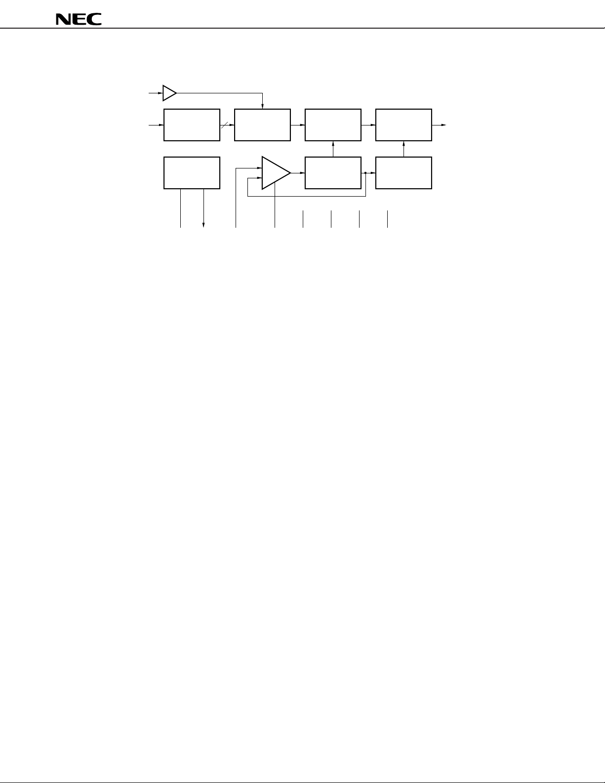
BLOCK DIAGRAM
CLK
D1 to D10 Input buffer
10
Master-slave
F.F.
Current switch R-2R ladder A
OUT
µ
PC667
Reference
voltage
generator
V
RSETVROUT
Amp.
V
REF
COMP AVCCDVCCAGND DGND
Reference
current source
Reference
resistor
2
Page 3
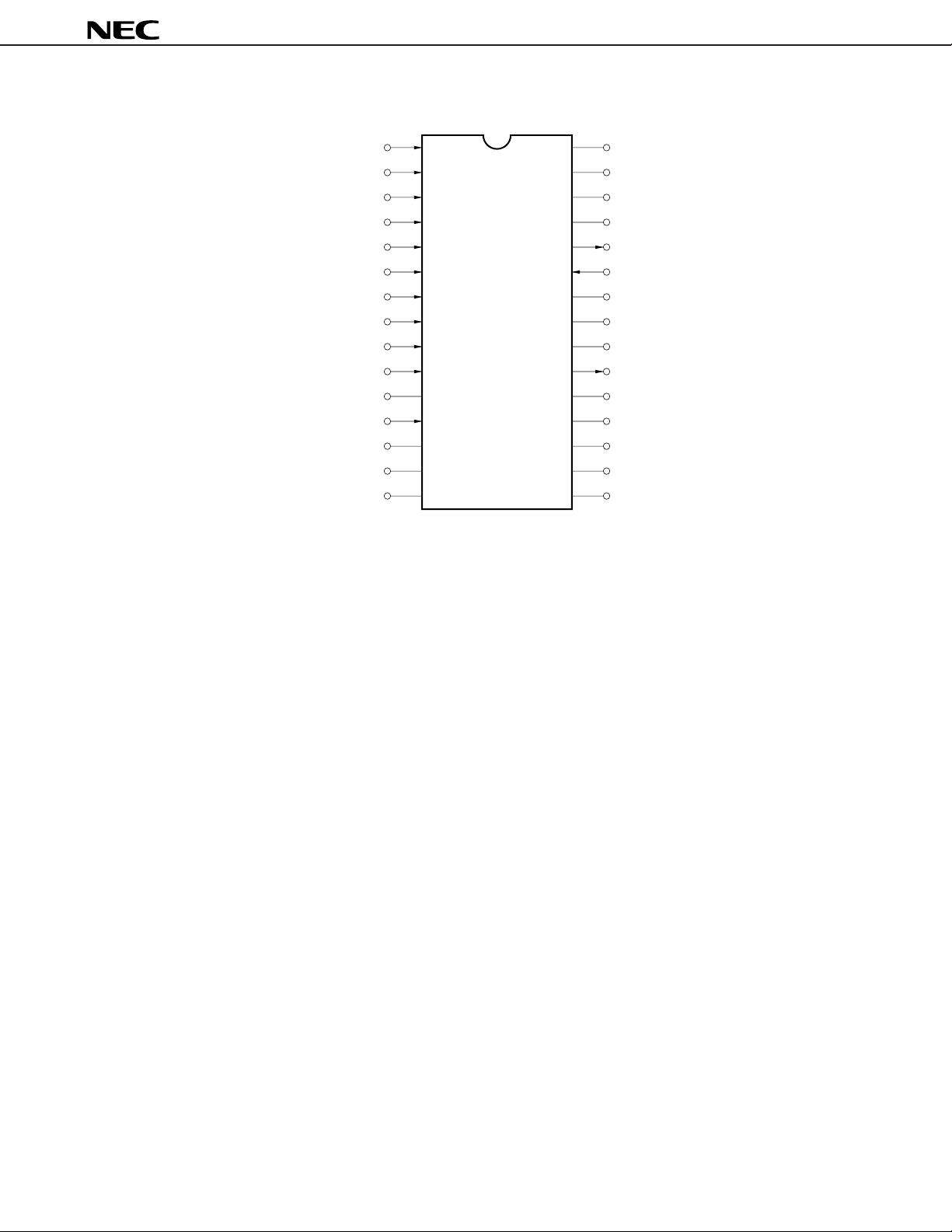
PIN CONFIGURATION (Top View)
µ
PC667
D1
D2
D3
D4
D5
D6
D7
D8
D9
D10
DGND
CLK
NC
DGND
NC
1
2
3
4
5
6
7
8
9
10
11
12
13
14
15
µ
PC667CT
30
29
28
27
26
25
24
23
22
21
20
19
18
17
16
AGND : Ground for Analog Circuit
AOUT : Analog Output
AVCC : Power Supply for Analog Circuit
CLK : Clock
COMP : Phase Compensation
D1 to D10 : Digital Signal
DGND : Ground for Digital Circuit
CC : Power Supply for Digital Circuit
DV
NC : No Connection
REF : Reference Voltage
V
VROUT : Reference Voltage Output
VRSET : Reference Voltage Adjustment
DV
CC
AGND
CC
AV
COMP
OUT
A
V
REF
AV
CC
AGND
DGND
ROUT
V
V
RSET
NC
NC
NC
NC
3
Page 4
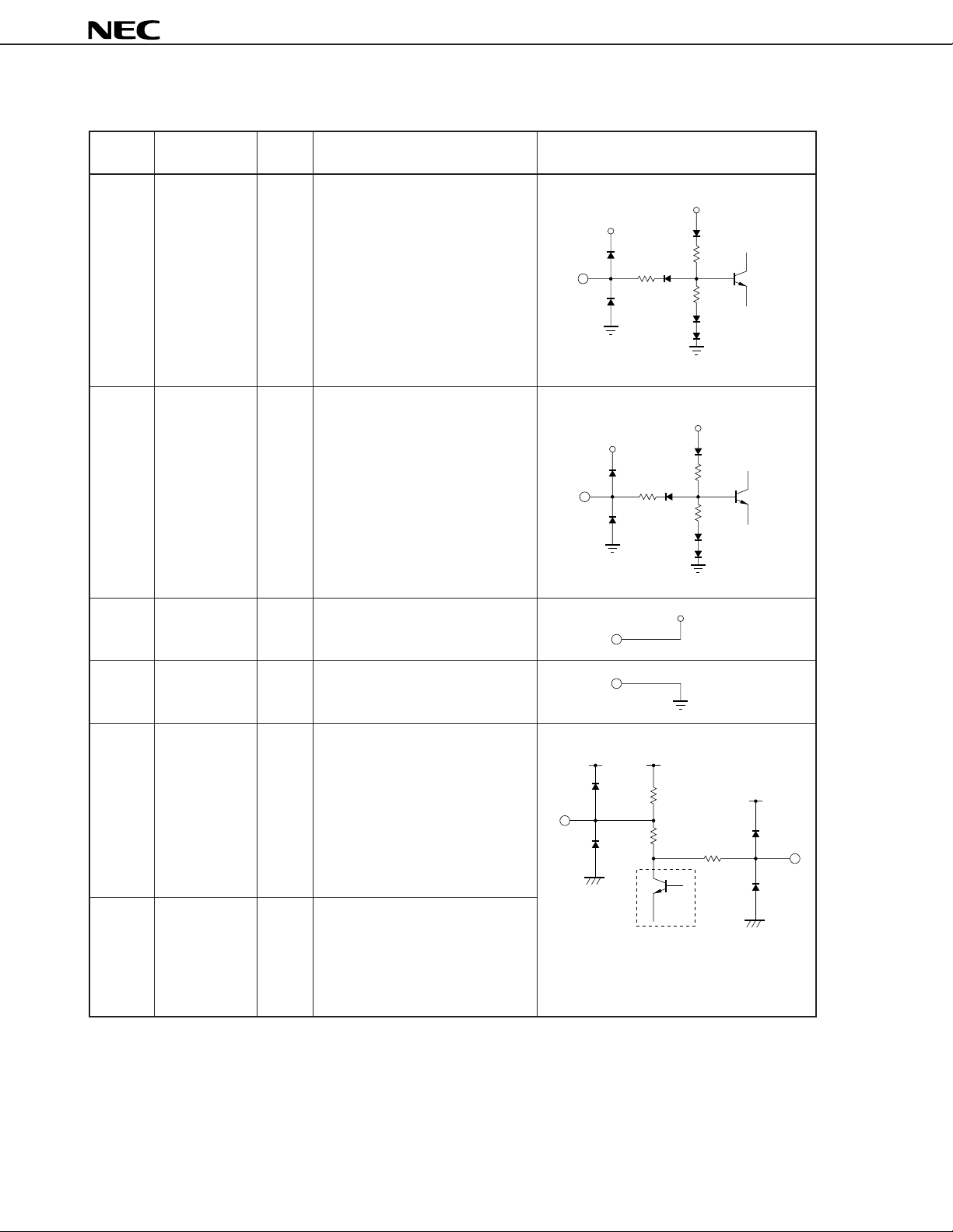
PIN FUNCTIONS
DV
CC
500 Ω
DGND
DGND
DV
CC
DV
CC
500 Ω
DGND
DGND
DV
CC
DVCC
DGND
µ
PC667
Pin Name Pin No.
D1 to D10
1 to 10 Input Digital signal
Input/
Output
D1 is MSB, D10 is LSB.
CLK 12 Input Clock
The rising edge of signal input to
this pin triggers analog output.
Function Equivalent Circuit
DVCC 30 — Power supply for digital circuit
DGND 11, 14, 22 — Ground for digital circuit
VRSET 20 — Reference voltage adjustment
Voltage adjusting pin for the
AV
CC
AV
CC
incorporated reference voltage
generating circuit. The output
7.5 kΩ
AV
CC
voltage of VROUT pin varies according
to the voltage applied to this pin.
When no adjustment is necessary,
connect approx. 0.1 µF capacitance
between this pin and GND pin.
VROUT 21 Output Reference voltage output
Voltage output pin of the incorporated reference voltage generating
V
ROUT
Reference
voltage
generator
AGND
3 kΩ
2 kΩ
RSET
V
AGND
circuit. This pin has high output
impedance, and must be connected
with a high impedance element.
4
Page 5
µ
AGND
AGND
5 kΩ
20 A
µ
AV
CC
AGND
PC667
Pin Name Pin No.
Input/
Output
Function Equivalent Circuit
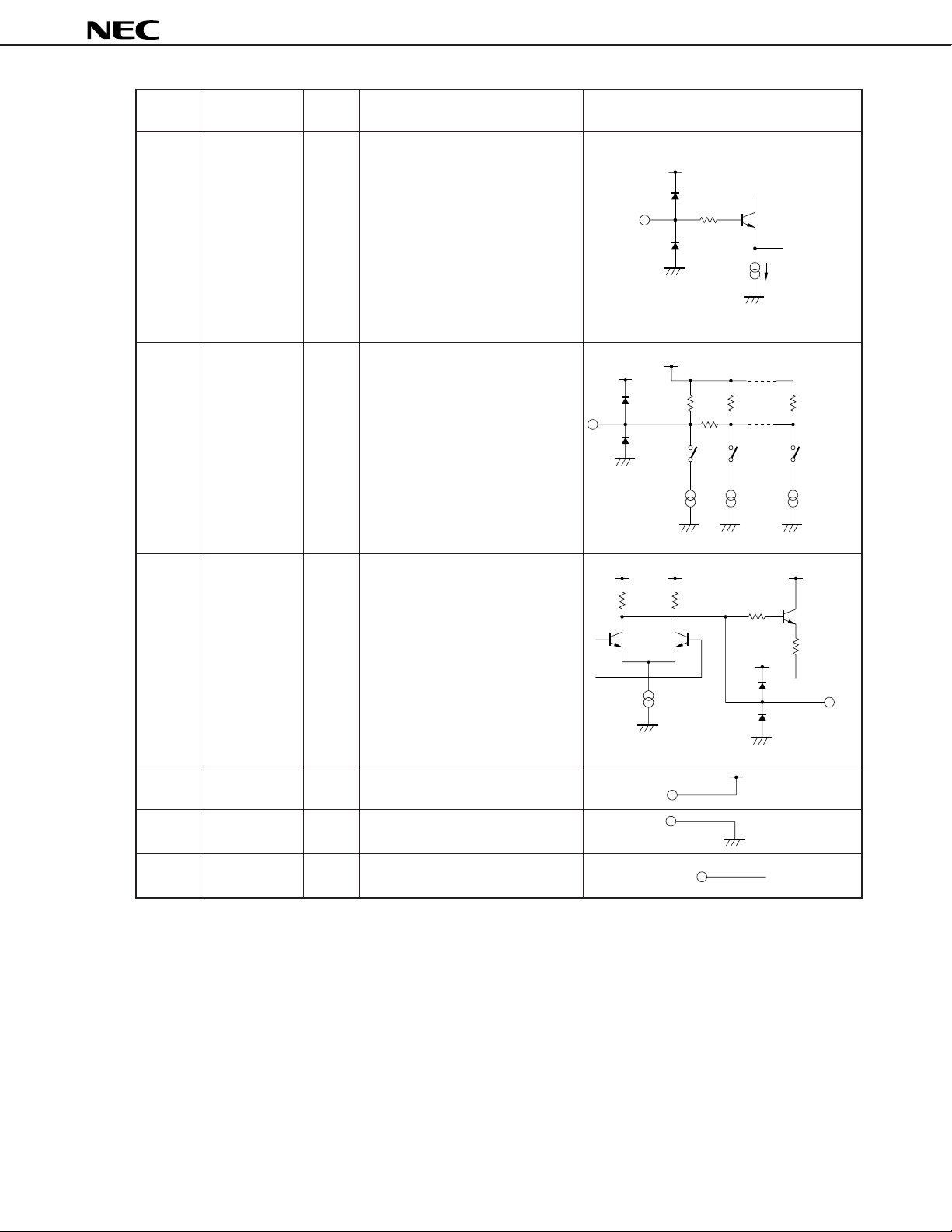
VREF 25 Input Reference voltage
The output full-scale range is set
according to the voltage applied to
this pin. Apply standard 4.0 V.
When no adjustment is necessary,
connect the output from VROUT pin
directly to this pin.
AOUT 26 Output Analog signal
Analog signal output pin.
COMP 27 — Phase compensation
Phase compensating capacitor
connection pin for full-scale amplifier. Approx. 0.1 µF capacitor must
be connected between this pin and
AVCC pin.
AV
AV
CC
112.5 Ω
AGND
AV
CC
AV
9.7 kΩ 9.7 kΩ
CC
CC
112.5 Ω
225 Ω
AV
CC
AGNDAGNDAGND
AV
112.5 Ω
R-2R
Ladder
resistance
CC
AVCC 24, 28 — Power supply for analog circuit
AGND 23, 29 — Ground for analog circuit
NC 13, 15 to 19 — No Connection
AGND
AGND
AV
CC
COMP
5
Page 6
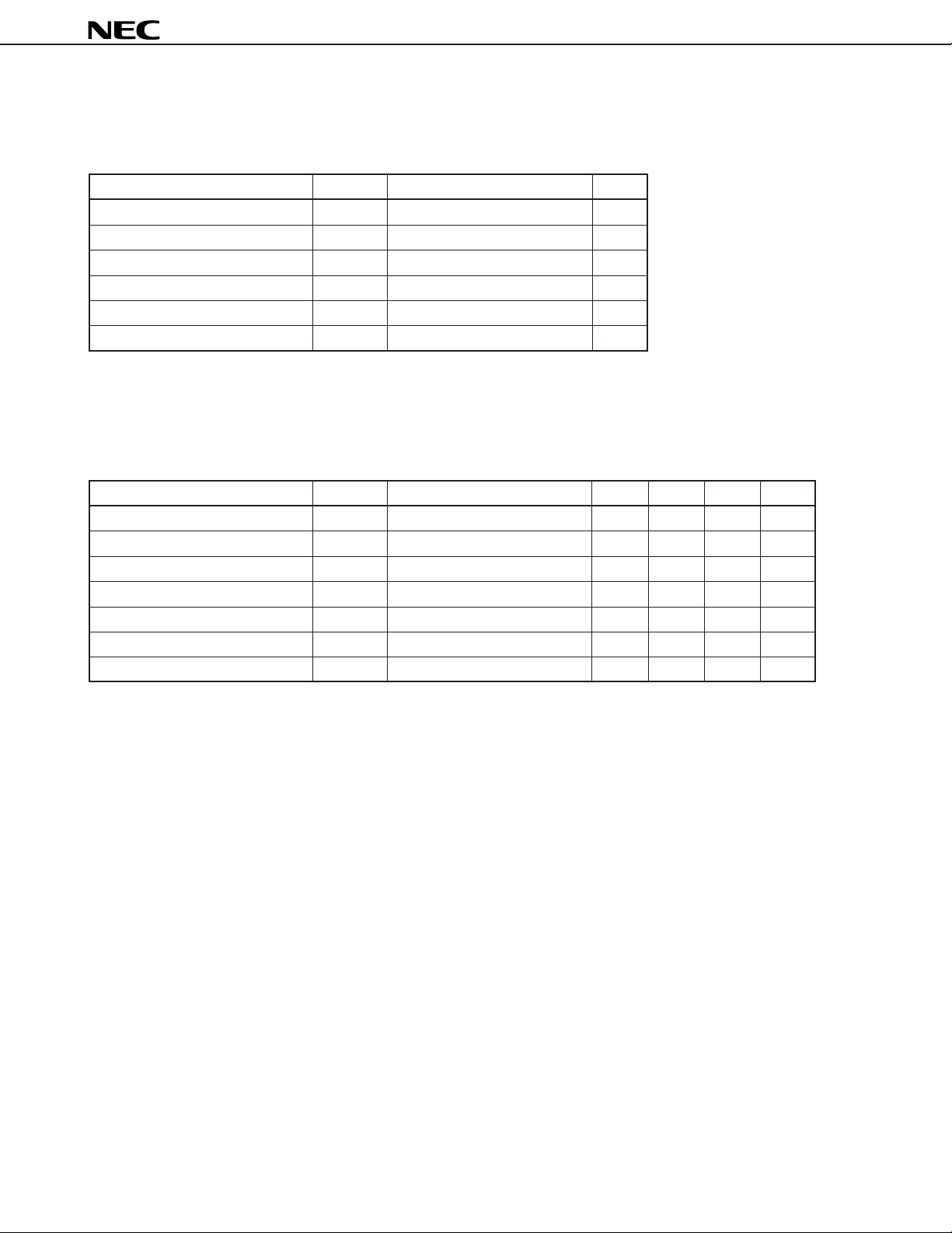
ELECTRICAL SPECIFICATIONS
Absolute Maximum Ratings (TA = 25 ˚C)
Parameter Symbol Ratings Unit
Supply voltage for digital circuit DVCC –0.3 to +6.0 V
Input voltage VI –0.3 to VCC +0.3 V
Operating ambient temperature TA –20 to +70 ˚C
Storage temperature Tstg –40 to +125 ˚ C
Power dissipation PD 0.8 (TA = +60 ˚C) W
Supply voltage for analog circuit AVCC DVCC –0.3 to DVCC +0.3 V
µ
PC667
★
Caution Exposure to Absolute Maximum Rating for extended periods may affect device reliability;
exceeding the ratings could cause permanent damage. The parameters apply independently.
Recommended Operating Conditions
Parameter Symbol Conditions MIN. TYP. MAX. Unit
Supply voltage for digital circuit DVCC 4.75 5.0 5.25 V
Supply voltage for analog circuit AVCC 4.75 5.0 5.25 V
Reference voltage input pin voltage VREF 3.8 4.0 4.2 V
High-level voltage of digital input VIH 2.0 V
Low-level voltage of digital input VIL 0.8 V
Conversion clock frequency fCLK 60 MHz
Phase compensation capacitance CCOMP 1.0
µ
F
6
Page 7
µ
PC667
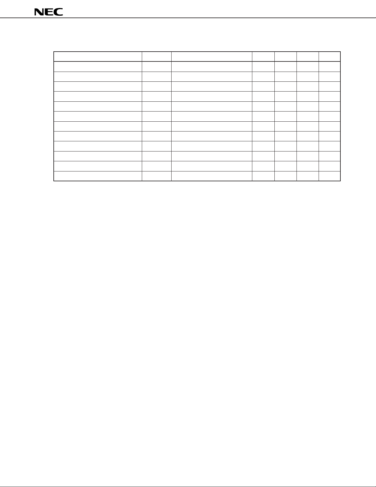
DC Characteristics and AC Characteristics (TA = –10 to +70 ˚C, DVCC = AVCC = +5 ±0.25 V)
Parameter Symbol Conditions MIN. TYP. MAX. Unit
Resolution RSL 10 Bit
Integral linearity error ILE TA = 0 to 60 ˚C, VREF = 4.0 V –1.0 +1.0 LSB
Differential linearity error DLE TA = 0 to 60 ˚C, VREF = 4.0 V –1.0 +1.0 LSB
Supply current ICC 50 71 mA
Set-up time ts 37ns
Hold time th 1.5 7 ns
Settling time tSET
Output delay time td VREF = 4.0 V 9 13 ns
Full-scale voltage output Vofs VREF = 4.0 V, RL > 100 kΩ 4.95 5.0 V
Zero-scale voltage output Vozs VREF = 4.0 V, RL > 100 kΩ 3.95 4 4.05 V
Output resistance Zout VREF = 4.0 V 70 85 100 Ω
Internal reference voltage output voltage
VROUT AVCC = 5.0 V 3.8 4.0 4.2 V
TA = 25 ˚C, RL = 375 Ω, VREF = 4.0 V
13 ns
Cautions 1. As for the phase compensation capacitance, capacitor of 1 µF should be connected between
the phase compensation capacitance pin (COMP) and the power supply pin for analog circuit
(AVCC).
2. The internal reference voltage output pin (V
ROUT) and the reference voltage input pin (VREF)
should be shorted.
3. The power supply and GND lines for analog circuit (AVCC and AGND) and those for digital
circuit (DV
CC and DGND) should be located as separately as possible.
7
Page 8
µ
PC667
★
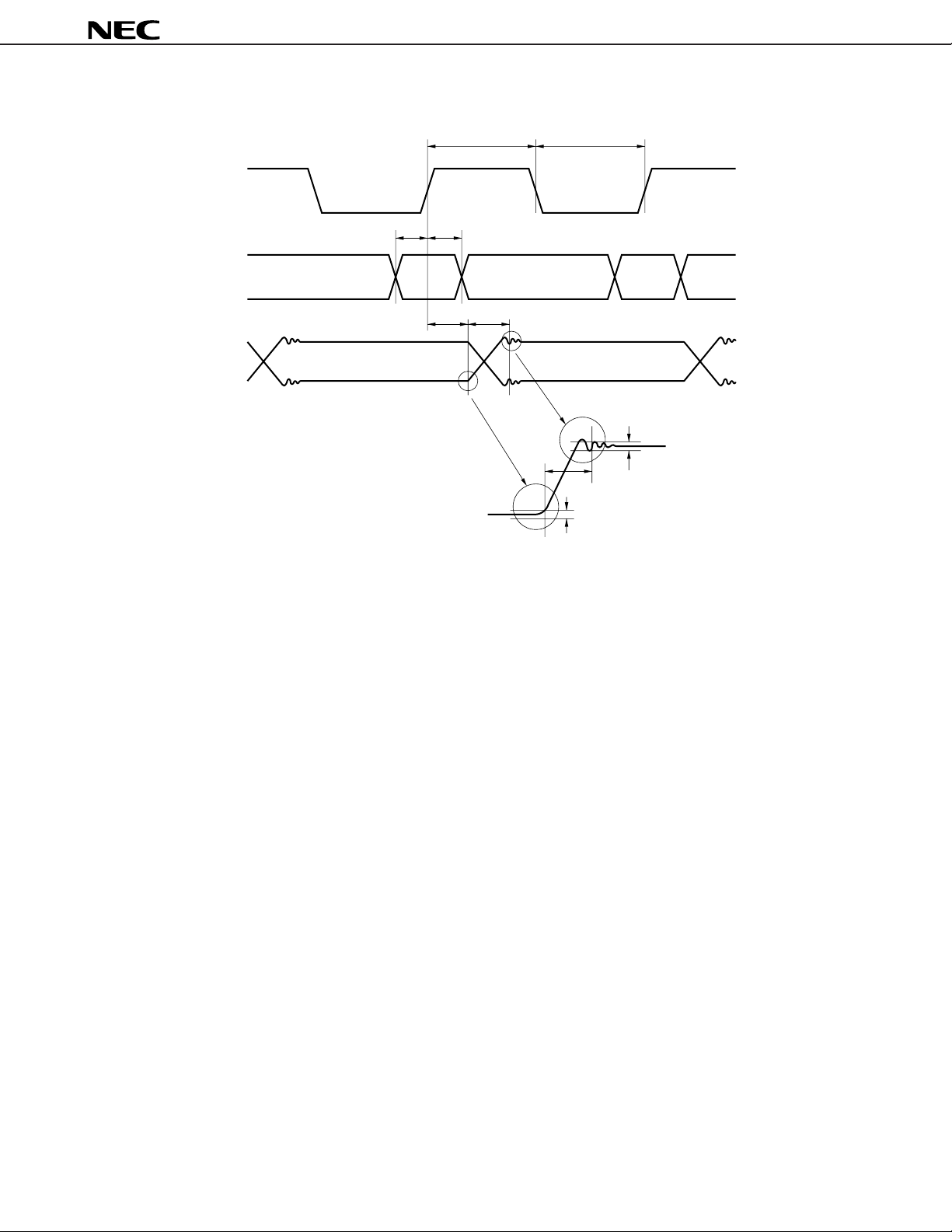
Timing Chart
t
PWH
t
PWL
CLK
tst
h
D
D1 to D10
A
OUT
n
t
SET
t
D
A
n-1
D
n+1
A
n
A
n+1
Final value ± 1/2 LSB
SET
t
± 1/2 LSB
8
Page 9
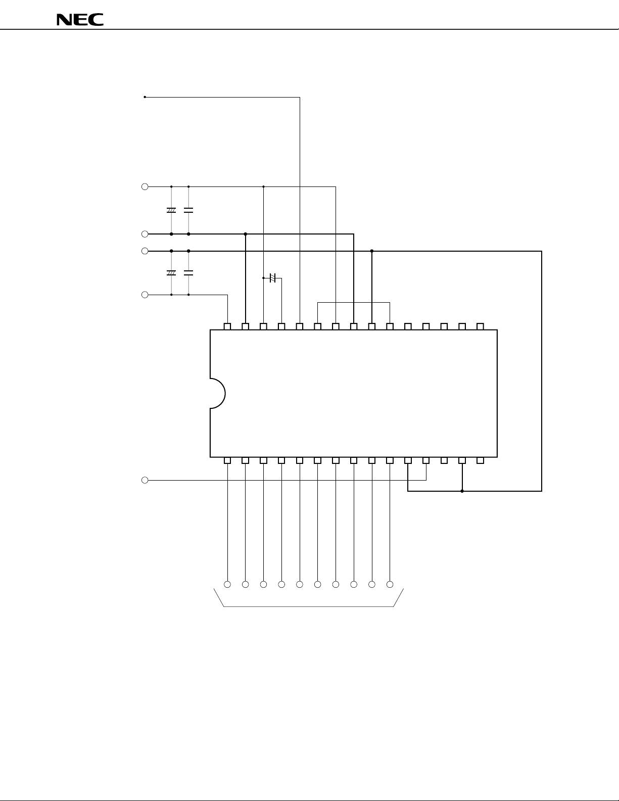
APPLICATION CIRCUIT EXAMPLE
Analog output
Power supply for
analog circuit
++
µµ
4.7 F
AGND
DGND
1000 pF
µ
PC667
4.7 F
Power supply for
digital circuit
Conversion clock
1000 pF
CC
DV
AGND
CC
AV
D1 (MSB)D2D3
+
µ
1 F
COMP
D4
OUT
A
D5
REF
V
D6
CC
AV
PC667CT
µ
D7
AGND
D8
DGND
D9
RSET
ROUT
V
V
D10 (LSB)
DGND
NC
CLK
NC
NC
NC
DGND
NC
NC
10-bit digital input
9
Page 10
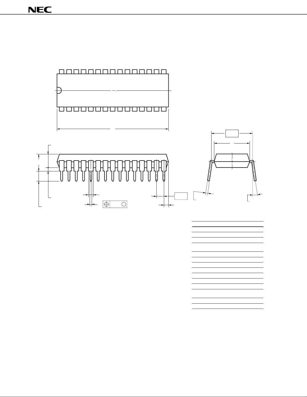
PACKAGE DRAWING
30PIN PLASTIC SHRINK DIP (400 mil)
30 16
115
µ
PC667
A
I
J
H
G
NOTES
1) Each lead centerline is located within 0.17 mm (0.007 inch) of
its true position (T.P.) at maximum material condition.
2) ltem "K" to center of leads when formed parallel.
F
DN
M
C
B
K
L
M
ITEM MILLIMETERS INCHES
A 28.46 MAX. 1.121 MAX.
B 1.78 MAX. 0.070 MAX.
C 1.778 (T.P.) 0.070 (T.P.)
D 0.50±0.10 0.020
F 0.85 MIN. 0.033 MIN.
G 3.2±0.3 0.126±0.012
H 0.51 MIN. 0.020 MIN.
I 4.31 MAX. 0.170 MAX.
J 5.08 MAX. 0.200 MAX.
K 10.16 (T.P.) 0.400 (T.P.)
L 8.6 0.339
M 0.25 0.010
N 0.17 0.007
R 0~15° 0~15°
+0.10
–0.05
R
+0.004
–0.005
+0.004
–0.003
S30C-70-400B-1
10
Page 11
µ
PC667
RECOMMENDED SOLDERING CONDITIONS
When soldering this product, it is highly recommended to observe the conditions as shown below. If other soldering
processes are used, or if the soldering is performed under different conditions, please make sure to consult with our
sales offices.
For more details, refer to our document “SEMICONDUCTOR DEVICE MOUNTING TECHNOLOGY MANUAL”
(IEI-1207).
Through-hole device
µ
PC667CT: 30-pin plastic Shrink DIP (400 mil)
Process Conditions
Wave soldering Solder temperature: 260 ˚C or below,
(only to leads) Flow time: 10 seconds or less.
Partial heating method Terminal temperature: 300 ˚C or below,
Heat time: 3 seconds or less (Per each lead).
★
Caution For through-hole devices, the wave soldering process must be applied only to leads, and make
sure that the package body does not get jet soldered.
11
Page 12

µ
[MEMO]
The application circuits and their parameters are for references only and are not intended for use in actual design-in's.
No part of this document may be copied or reproduced in any form or by any means without the prior written
consent of NEC Corporation. NEC Corporation assumes no responsibility for any errors which may appear in this
document.
NEC Corporation does not assume any liability for infringement of patents, copyrights or other intellectual
property rights of third parties by or arising from use of a device described herein or any other liability arising
from use of such device. No license, either express, implied or otherwise, is granted under any patents,
copyrights or other intellectual property rights of NEC Corporation or others.
While NEC Corporation has been making continuous effort to enhance the reliability of its semiconductor devices,
the possibility of defects cannot be eliminated entirely. To minimize risks of damage or injury to persons or
property arising from a defect in an NEC semiconductor device, customer must incorporate sufficient safety
measures in its design, such as redundancy, fire-containment, and anti-failure features.
NEC devices are classified into the following three quality grades:
“Standard“, “Special“, and “Specific“. The Specific quality grade applies only to devices developed based on
a customer designated “quality assurance program“ for a specific application. The recommended applications
of a device depend on its quality grade, as indicated below. Customers must check the quality grade of each
device before using it in a particular application.
Standard: Computers, office equipment, communications equipment, test and measurement equipment,
audio and visual equipment, home electronic appliances, machine tools, personal electronic
equipment and industrial robots
Special: Transportation equipment (automobiles, trains, ships, etc.), traffic control systems, anti-disaster
systems, anti-crime systems, safety equipment and medical equipment (not specifically designed
for life support)
Specific: Aircrafts, aerospace equipment, submersible repeaters, nuclear reactor control systems, life
support systems or medical equipment for life support, etc.
The quality grade of NEC devices in “Standard“ unless otherwise specified in NEC's Data Sheets or Data Books.
If customers intend to use NEC devices for applications other than those specified for Standard quality grade,
they should contact NEC Sales Representative in advance.
Anti-radioactive design is not implemented in this product.
PC667
M4 94.11
 Loading...