

Page 1

DATA SHEET
BIPOLAR ANALOG INTEGRATED CIRCUIT
µ
PC7073
µ
PC7073 ANALOG SUBSCRIBER LINE LSI (BS-SLIC)
The µPC7073 is a BS-SLIC that can be used in analog subscriber circuits such as private branch exchangers
(PBXs) and switching equipment for central offices. It features two of the functions required for analog subscriber
circuits: subscriber line feed control and subscriber line supervision.
µ
Use of the
required in analog subscriber circuits.
FEATURES
• Single-chip, monolithic LSI (bipolar)
• Constant-resistance feed or semi constant-current feed
• 200-Ω feed, 400-Ω feed, or Tip-to-Ring pin feedout status (HIGH and WET)
• On-chip metering signal superposing circuit
• On-hook sending and receiving
• Loop detection
• Ground detection and ground-fault/power contact protection
• Three on-chip relay drivers (flyback prevention diode must be externally provided)
• Two power supply voltages (–48 V and +5 V)
• Low power consumption: 110 mW (TYP., when on hook)
PC7073 in combination with a digital CODEC (µPD9903) can reduce the number of components
Note
Note
Note
µ
Note Requires
ORDERING INFORMATION
Part Number Package
µ
PC7073GT 48-pin plastic shrink SOP (375 mil)
PD9903.
The information in this document is subject to change without notice.
Document No. S10896EJ2V0DS00 (2nd edition)
(Previous No. ID-3576)
Date Published June 1996 P
Printed in Japan
©
1996
Page 2
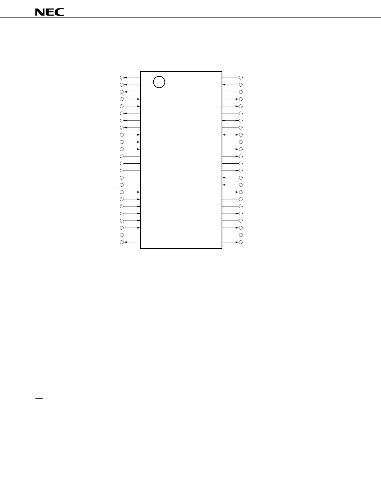
PIN CONFIGURATION
48-pin plastic shrink SOP (375 mil)
DC
OUT3
DC
OUT2
DC
OUT1
DC
IN1
DC
IN2
BB
OUT
ASCN
AGDT
BIAS
R
X
ACOM
NC
NC
NC
GND1
NC
PD
ALM
BCUT
1
RC
RC
2
RC
3
V
BB
T
EF
1
2
3
4
5
6
7
8
9
10
11
12
13
14
15
16
17
18
19
20
21
22
23
24
µ
PD7073GT
48
47
46
45
44
43
42
41
40
39
38
37
36
35
34
33
32
31
30
29
28
27
26
25
V
CC
TTX
C
PSR
R
B
R
E
NC
S
R
NC
T
S
NC
E
T
T
B
C
DC
T
X
OP
IN–
OP
IN+
R
EF
GND2
NC
3
RY
NC
2
RY
NC
1
RY
µ
PC7073
IN
ACOM : ANALOG COMMON VOLTAGE RB : RING BASE
AGDT : ANALOG GROUND DETECTION SIGNAL OUT RC
1-RC3 : RELAY CONTROL IN
ALM : ALARM IN RE : RING EMITTER
ASCN : ANALOG LOOP DETECTION SIGNAL OUT REF : RING EMITTER PROTECT FEED
OUT :VBB VOLTAGE INFORMATION OUT RS : RING SENSE
BB
BCUT : BATTERY FEED CUT SIGNAL IN RX : SIGNAL RECEPTION IN
BIAS : BIAS LEVEL RY1-RY3 : RELAY DRIVER OUT
CDC : DC FEEDBACK CAPACITOR T
B : TIP BASE
CPSR : POWER SUPPLY REJECTION CAPACITOR TE : TIP EMITTER
DCIN1, DCIN2 : DC FEEDBACK CONTROL IN TEF : TIP EMITTER PROJECT FEED
OUT1-DCOUT3 : DC FEEDBACK CONTROL OUT TS : TIP SENSE
DC
GND1, GND2 : GROUND TTXIN : TELETAX SIGNAL IN
NC : NO CONNECTION TX : TRANSSMISSION OUTPUT
IN+ : TELETAX SIGNAL CANCEL IN (+) VBB :
OP
NEGATIVE POWER SUPPLY (–48 V)
OPIN– : TELETAX SINGAL CANCEL IN (–) VCC : POSITIVE POWER SUPPLY (+5 V)
PD : POWER DOWN CONTROL IN
2
Page 3
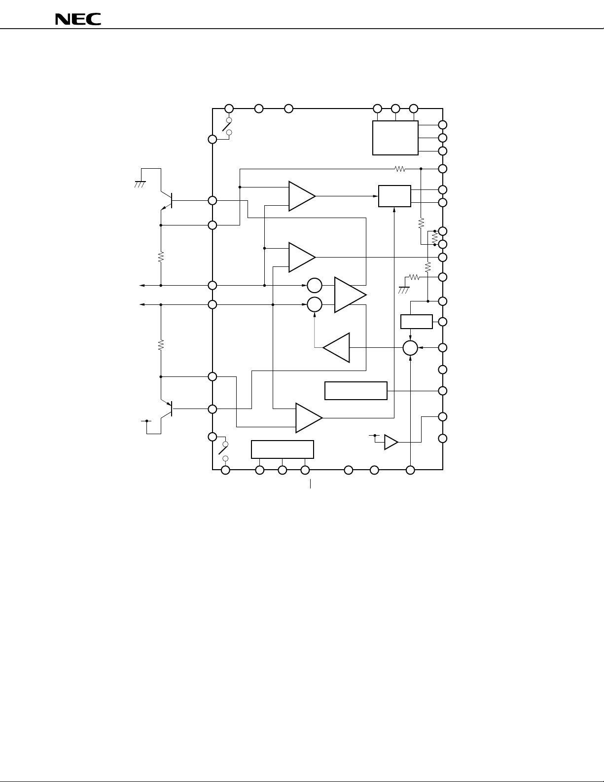
BLOCK DIAGRAM
µ
PC7073
RY
3
RY
2
RY
GND2V
GND1
T
EF
CC
1
Relay
drivers
RC
RC
RC
DC
1
2
3
OUT2
Tip
Ring
T
B
T
E
T
S
R
S
+
+
Σ
L.P.F
+
R
E
Bias circuit
R
B
R
V
BB
EF
V
BB
AGDT
ASCN
DC
OUT3
DC
OUT1
T
X
DC
IN1
DC
IN2
CDC
R
X
BIAS
ACOM
BB
OUT
C
PSR
Logic circuits
V
BB
BCUT
ALM
PD
OP
IN–OPIN+
TTX
IN
3
Page 4

µ
PC7073
CONTENTS
1. PIN FUNCTIONS ............................................................................................................................. 5
2. USE CAUTIONS.............................................................................................................................. 7
3. ELECTRICAL SPECIFICATIONS ................................................................................................... 8
3.1 Discrete unit ratings............................................................................................................................... 8
3.2 Combined specifications with µPD9903 .............................................................................................. 10
4. SYSTEM APPLICATION EXAMPLE USING µPC7073 AND µPD9903 .................................... 14
5. PACKAGE DRAWING ..................................................................................................................... 15
6. RECOMMENDED SOLDERING CONDITIONS ............................................................................ 16
4
Page 5
µ
PC7073
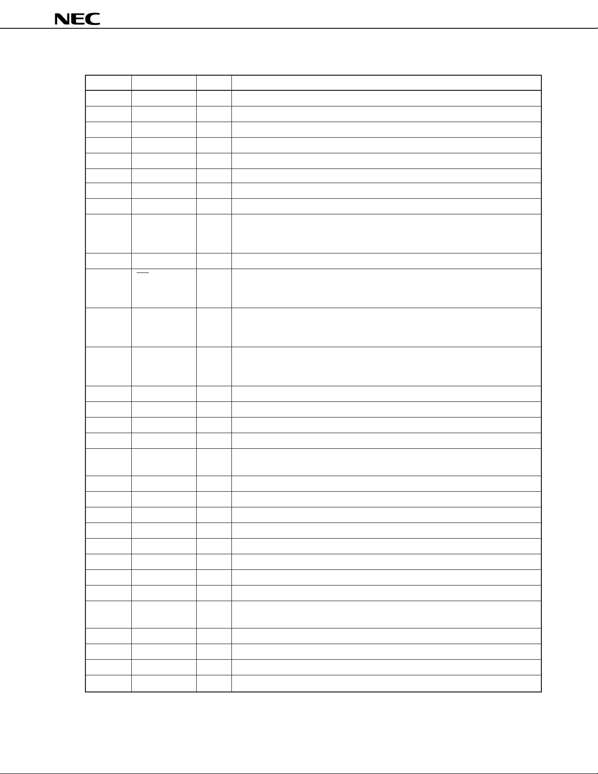
1. PIN FUNCTIONS
Number Pin Name I/O Function
1-3 DCOUT1-DCOUT3 O DC feedback control output [to the µPD9903’s pin 48-46]
4, 5 DCIN1, DCIN2 I DC feedback control input [to the µPD9903’s pin 45, 44]
6BBOUT OVBB voltage information output [to the µPD9903’s pin 43]
7 ASCN O Tip-Ring difference current detection signal output [to the µPD9903’s pin 42]
8 AGDT O Tip-Ring sum current detection signal output [to the µPD9903’s pin 41]
9 BIAS I Bias level input. Connect to µPD9903’s AIN pin [to the µPD9903’s pin 40]
10 RX I Receiving input for 4W side [to the µPD9903’s pin 39]
11 ACOM I
12-14, 16, NC – No-connection pins. Leave these pins unconnected.
26, 28, 30,
39, 41, 43
15 GND1 – Ground pin 1, for circuit grounding
17 PD I Power-down control
18 ALM I Ground-fault/power line contact protection mode select input
19 BCUT I Feed-out select input
20 RC1 I Relay control for ringer transmission, high active [to the µPD9903’s pin 29]
21 RC2 I Relay control for line test, high active [to the µPD9903’s pin 28]
22 RC3 I Relay control for network test, high active [to the µPD9903’s pin 27]
23 VBB – Negative power supply (–48 V)
24 TEF O Feed resistor pin connection for Tip side during ground-fault/power line contact
25 RY1 O Relay control for ringer transmission, open collector
27 RY2 O Relay control for line testing, open collector
29 RY3 O Relay control for network testing, open collector
31 GND2 – Ground pin 2, relay driver
32 REF O
33 OPIN+ I TTX (Teletax) signal cancel circuit input pin (+)
34 OPIN– I TTX signal cancel circuit input pin (–)
35 TX O Transmission output for 4W side. Connect with BIAS pin via CAC capacitor.
36 CDC – Connect to DC feedback capacitor
37 TB O Tip-side auxiliary power transistor base connection pin
38 TE O Tip-side feed amplifier output pin. Connect with TS pin via RFT resistor.
40 TS I/O Tip pin for 2W side
42 RS I/O Ring pin for 2W side
Signal reference voltage (2.4 V TYP) input for 4W side
H: Power-up
L: Power-down [to the µPD9903’s pin 32]
H: Protect mode
L: Normal feed [to the µPD9903’s pin 31]
H: Feed-out
L: Normal feed [to the µPD9903’s pin 30]
detection
Ring feed resistor pin connection for ground-fault/power line contact detection
Connect CDC capacitor to this pin
TTL level
TTL level
TTL level
[to the µPD9903’s pin 37, 38]
5
Page 6

Number Pin Name I/O Function
44 RE O Ring-side feed amplifier output pin. Connect with RS pin via RFR resistor.
45 RB O Ring-side auxiliary power transistor base connection pin
46 CPSR – Connect a capacitor for power supply noise eliminator
47 TTXIN I TTX signal input pin
48 VCC – Positive power supply (+5 V)
µ
PC7073
6
Page 7

µ
PC7073
2. USE CAUTIONS
(1) Combined characteristics of µPC7073 and µPD9903
• The µPC7073 is designed to be used in combination with the µPD9903. Therefore, first half of the electrical
µ
characteristics described below are ratings for the
combined ratings that include the µPD9903.
• Subscriber circuit constants that are determined by factors such as termination impedance are configured to
enable setting by external order parameters. Consequently, input of an order that is not suitable for the target
impedance may result in failure to obtain the required characteristics.
(2) Absolute maximum ratings
Application of voltage or current in excess of the absolute maximum ratings may result in damage. Be
especially cautious about surges, etc.
(3) Load of by-pass capacitor
µ
Because the
supply impedance can cause instability (such as oscillation) in these internal operational amplifiers. To
suppress such instability and eliminate power supply noise, connect by-pass capacitors (CACOM = approx.
µ
F) having superior high frequency characteristics as close as possible to the µPC7073’s power supply
0.1
pins (VBB and VCC) and the µPD9903’s power supply pins (AVDD and DVDD).
PC7073 and µPD9903 use several internal high-frequency operational amplifiers, high power
PC7073 as a discrete unit while the second half are
(4) Addition of ACOM pin connection capacitor
µ
The voltage of the ACOM pin between the
for the µPC7073. Superposition of noise on this pin may have adverse effects on transmission characteristics. Therefore, make the wires between the ACOM pin and the two LSIs as short as possible, and connect
capacitors (C
the pins.
(5) Overcurrent prevention measures
Due to its structure, power to the
Accordingly, if power is supplied first to a power supply pin other than V
the µPC7073 (an overcurrent will not flow if power is input to all power supply pins).
Therefore, if feeding to a power supply pin other than VBB first, connect an external diode and limiting resistor
(rated at several Ω) in the directions described below.
• Reverse-bias direction between V
• Reverse-bias direction between V
• Reverse-bias direction between VCC pin and GND.
ACOM = approx. 0.1
µ
F) having superior high frequency characteristics as close as possible to
µ
BB pin and VCC pin.
BB pin and GND.
PC7073 and µPD9903 is the signal source reference voltage
PC7073 must first be supplied to a low-voltage potential (VBB).
BB, an overcurrent will flow within
7
Page 8
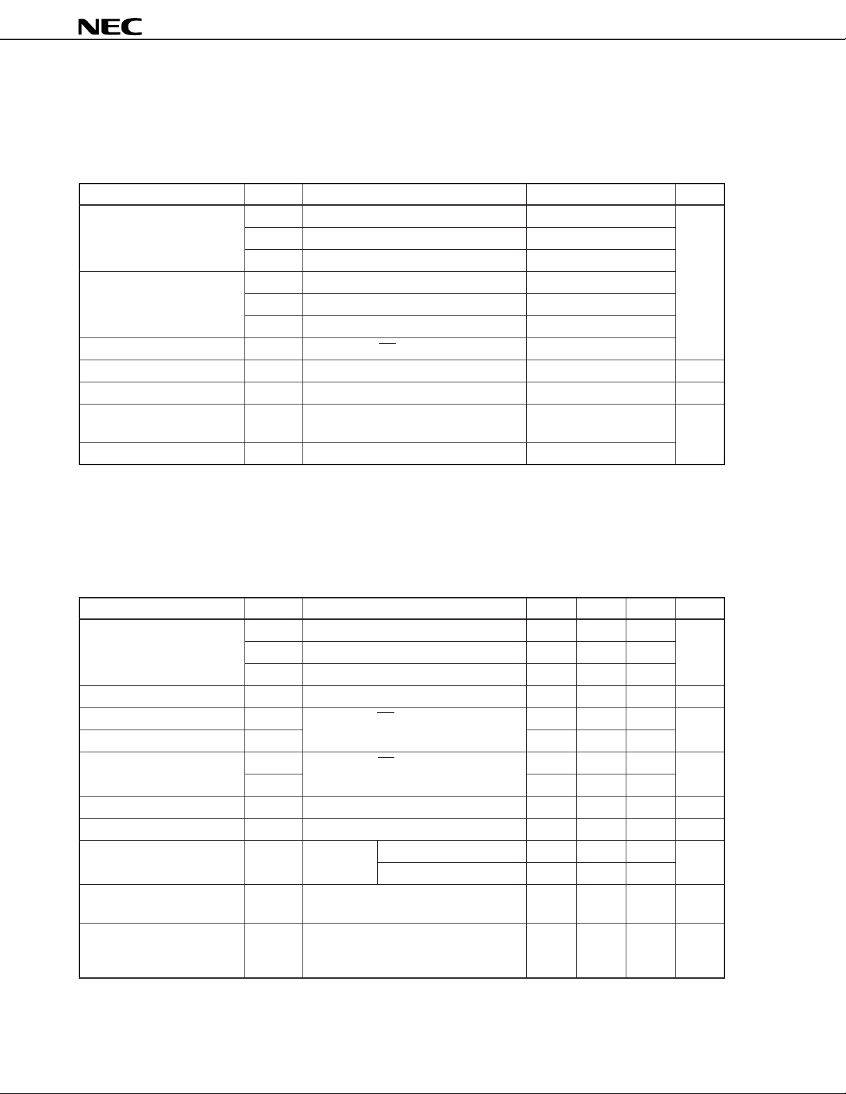
3. ELECTRICAL SPECIFICATIONS
3.1 Discrete unit ratings
Absolute maximum ratings (TA = +25 °C)
Parameter Symbol Conditions Rating Units
Power supply voltage VBB Including spike voltage –63 to +0.3 V
VCC Including spike voltage –0.3 to +7.0
VACOM ACOM pin –0.3 to VCC + 0.3
Input voltage VIN0 RX pin –0.3 to VCC + 0.3
VIN1 TS, RS, TE, and RE pins VBB – 0.3 to VCC + 0.3
VIN2 TTXIN pin To be defined
Logic input voltage VIN3 BCUT, ALM, PD, RC1, RC2, and RC3 pins –0.3 to VCC + 0.3
Relay driver output current IOL RY1, RY2, and RY3 pins 40 mA
Power consumption PT
Ambient operating TA 0 to 70 ˚C
temperature
Storage temperature Tstg –65 to +150
Thermal resistance: 160 °C/W, TA = 70 °C
1W
µ
PC7073
Caution If the absolute maximum rating for any of the above parameters is exceeded even momentarily,
it may adversely affect the quality of this product. In other words, these absolute maximum
ratings have been set to prevent physical damage to the product. Do not use the product in such
a way as to exceed any of these ratings.
Recommended operating conditions
Parameter Symbol Conditions MIN. TYP. MAX. Units
Power supply voltage VBB –58 –48 –42 V
VCC 4.75 5.0 5.25
VACOM ACOM pin 2.38 2.4 2.42
Ambient operating temperature
High level input voltage VIH BCUT, ALM, PD, RC1, RC2, and RC3 pins 2.0 VCC V
Low level input voltage VIL 0 0.8
Digital input rise and fall times
RX drive impedance 050Ω
RX-ACOM offset voltage –0.1 +0.1 V
Loop resistance (line resistance
+ termination resistance)
Terminal leakage current ION-LEAK 08mA
during on-hook transmission
AC inductive current Ilong f = 60 Hz, 2Pw-Tr
TA 0 2570˚C
tR BCUT, ALM, PD, RC1, RC2, and RC3 pins 200 ns
tF 200
RL VBB = –51 V 200 Ω × 2 feeding modes 1900 Ω
400 Ω × 2 feeding modes 1500
Note
During loop detection (one line),
during ground detection (one line)
5.0 mArms
Note Pw-Tr is a power transistor for feeding.
8
Page 9
µ
PC7073
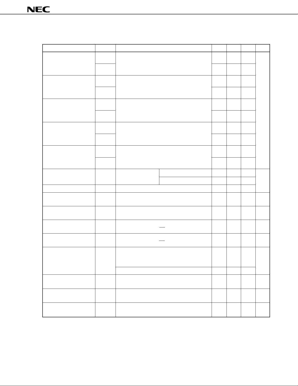
DC Characteristics
(VBB = –42 to –58 V, VCC = 5 V ± 0.25 V, TA = 0 to 70 ˚C, combined characteristics with µPD9903)
Parameter Symbol Conditions MIN. TYP. MAX. Units
On-hook supply current 1 IBB1 On-hook, including IPw-Tr
CC1
I
Ilong = 0 mA, VBB = –48 V
Off-hook supply current 1 IBB2 Off-hook, not including IPw-Tr
CC2
I
On-hook supply current 2 IBB3
CC3
I
Off-hook supply current 2 IBB4
CC4
I
Power current during IBB6
on-hook transmission
CC6
I
Ilong = 0 mA, VBB = –48 V
On-hook, including IPw-Tr
Ilong = 0 mA, VBB = –58 V
Off-hook, not including IPw-Tr
Ilong = 0 mA, VBB = –58 V
On-hook, including IPw-Tr
Ilong = 0 mA, VBB = –58 V
ACOM input current IACOM ACOM pin On-hook –100 –16 +100
RX input current IRX RX, VRX = 2.4 V 8 12 16
Relay driver input IIH VI = 5.0 V 1.0 1.5 mA
current For each RC1, RC2, and RC3 pins
Relay driver output VOL IOL = 35 mA +1.1 V
voltage For each RY1, RY2, and RY3 pins
Digital pin high level IIH VI = 2.0 V 0.5 mA
input current For each BCUT, ALM, PD, RC1, RC2, and RC3 pins
Digital pin low level IIL VI = 0.0 V 50
input current For each BCUT, ALM, PD, RC1, RC2, and RC3 pins
Control input voltage BCUT : IL = 50 mA → | IL | ≤ 1 mA 2.0 V
: IL = 50 mA → – IL × 90 %
: IL = 50 mA → | IL | ≤ 20 mA
BCUT, IL = 50 mA → – IL × 90 % 0.8
Note
IL = 0 mA 1.9 mA
1
VCC = +5 V
Note
IL = 20 mA 4.3
2.0
VCC = +5 V
Note
IL = 0 mA
2.3 2.9
1.3 1.7
VCC = +5.25 V
Note
IL = 20 mA
4.4 5.5
2.2 2.8
VCC = +5.25 V
Note
IL = 0 mA
3 3.9
2.1 2.7
VCC = +5.25 V
Off-hook –100 0 +100
µ
A
µ
A
DC feed resistance RBF 200 Ω feed 180 200 220 Ω
400 Ω feed 360 400 440
High and wet RH&W RL = 1900 Ω 100 kΩ
impedance AC/DC
Ground-fault/power VBB = –48 V 12.1 13.1 14.1 mA
contact drooping current RTE5K/RRE5K = 3.6 kΩ
Note IPw-Tr is the current to the power transistor for feeding.
9
Page 10
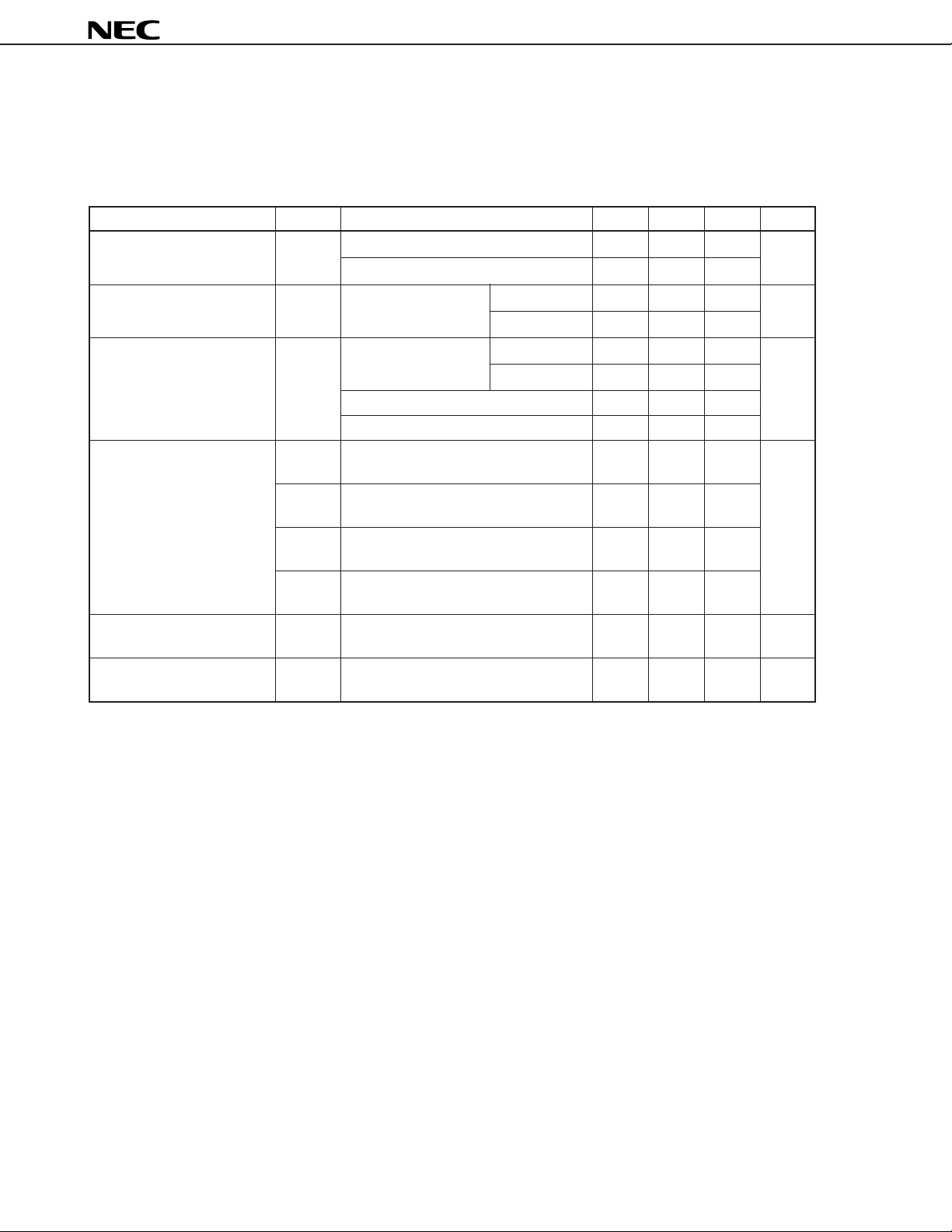
3.2 Combined specifications with µPD9903
DC characteristics
µ
PC7073 (VBB = –42 to –58 V, VCC = 5 V ± 0.25 V, TA = 0 to 70 ˚C, 18 ≤ IL ≤ ILMAX (mA))
µ
PD9903 (TA = 0 to 70 ˚C, VDD = 5 V ± 0.25 V, VDD = VAG = 0 V, fDCLK = 2048 kHz)
Parameter Symbol Conditions MIN. TYP. MAX. Units
DC feed resistance RBF 200 Ω feed 180 200 220 Ω
400 Ω feed 360 400 440
Minimum loop unit ILMIN VBB = –51 V 200 Ω feed 21.7 22.2 22.6 mA
RL = 1900 Ω 400 Ω feed 18.2 18.8 19.3
Maximum current setting ILMAX ILMAX = 76 mA setting 200 Ω feed 70 76 82 mA
400 Ω feed 50 55 60
ILMAX = 45 mA setting 40 45 50
ILMAX = 35 mA setting 31 35 39
Pin voltage during on-hook VTS Normally on-hook, 2.25 2.55 2.85 V
between Tip and GND, VBB = –48 V
VRS Normally on-hook, 3.05 3.35 3.65
between Ring and VBB, VBB = –48 V
VTS On-hook transmission, 2.25 2.55 2.85
between Tip and GND, VBB = –48 V
VRS On-hook transmission, 3.05 3.35 3.65
between Ring and VBB, VBB = –48 V
Voltage between lines VTS VBB = –48 V VBB – 7.0 VBB – 5.9 VBB – 5.0 V
during on-hook
Supervisory control VBBF 32 35 38 V
– VBB fault voltage
µ
PC7073
10
Page 11
µ
PC7073
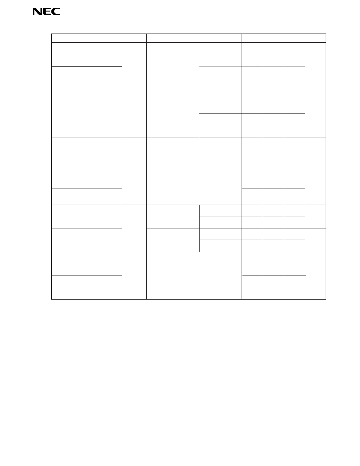
Parameter Symbol Conditions MIN. TYP. MAX. Units
Loop detection operating RON1 Includes termination 200 Ω feed 2500 Ω
resistance (during normal resistance 400 Ω feed 2100
transmission)
Loop detection non-operating 200 Ω feed 3900
resistance (during normal 400 Ω feed 3500
transmission)
Loop detection operating RON2 Includes termination 200 Ω feed 1900 Ω
resistance (during on-hook resistance 400 Ω feed 1500
transmission)
Loop detection non-operating
resistance (during on-hook 400 Ω feed 2440
transmission)
Loop release non-operating RON3 Includes termination 200 Ω feed 2960 Ω
resistance resistance 400 Ω feed 2560
Loop release operating 200 Ω feed 4540
resistance 400 Ω feed 4140
Ground detection 1 (C/O) RON4 Includes termination resistance 5.2 kΩ
operating resistance
Ground detection 1 (C/O) 20
non-operating resistance
Ground-fault/power line RON6 Includes termination
contact detection resistance
operating resistance Off-hook stage
Ground-fault/power line Includes termination
contact detection non- resistance
operating resistance
Ground-fault/power line RON7 Includes termination resistance 1.4 kΩ
contact release nonoperating resistance
Ground-fault/power line 10
contact release operating
resistance
200 Ω feed 2840
LMAX
I
= 45/76 mA 340
I
= 35 mA 480
LMAX
LMAX
I
= 45/76 mA 870
I
= 35 mA 1130
LMAX
Ω
Ω
Note The above values are resistance-converted values.
11
Page 12
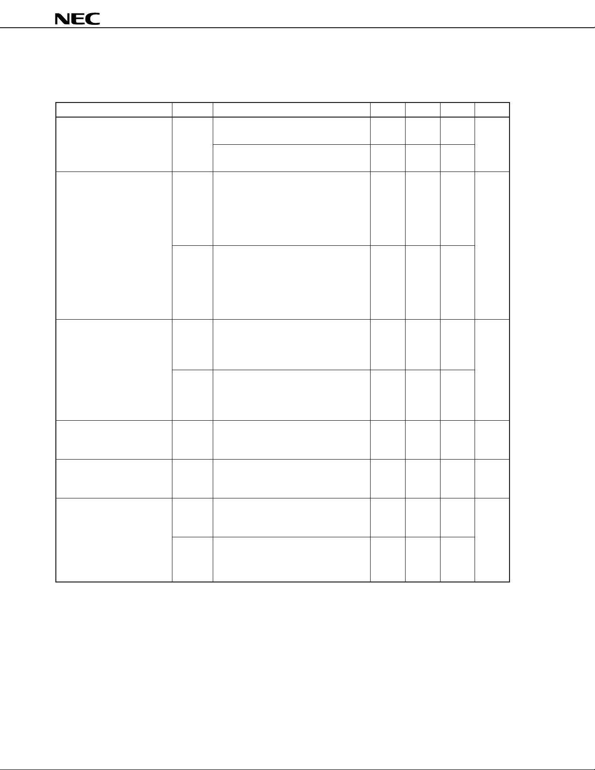
Transmission Characteristics
µ
PC7073 (VBB = –42 to –58 V, VCC = 5 V ± 0.25 V, TA = 0 to 70 ˚C, 18 ≤ IL ≤ ILMAX (mA))
µ
PD9903 (TA = 0 to 70 ˚C, VDD = 5 V ± 0.25 V, VDG= VAG = 0 V, fDCLK = 2048 kHz)
Parameter Symbol Conditions MIN. TYP. MAX. Units
Insertion loss IL A-D input signal –0.45 0.0 +0.45 dB
0 dBm0 1 kHz
D-A input signal –0.45 0.0 +0.45
0 dBm0 1 kHz
Transfer loss frequency FRX A-D 60 Hz 24.0 – dB
characteristics Reference input signal 200 Hz 0.6 2.0
1015 Hz 0 dBm0 300 Hz –0.15 +0.21
400 to 3000 Hz –0.15 +0.15
3200 Hz –0.15 +0.65
3400 Hz 0.2 0.8
FRR D-A 60 Hz 0.2 4.0
Reference input signal 200 Hz 0.1 1.0
1015 Hz 0 dBm0 300 Hz –0.15 +0.25
400 to 3000 Hz –0.15 +0.15
3200 Hz –0.15 +0.65
3400 Hz 0.2 0.8
Gain tracking GTX A-D +3 to –40 dBm0 –0.2 +0.2 dB
(tone method) Reference input signal –50 dBm0 –0.5 +0.5
–10 dBm0 –55 dBm0 –1.0 +1.0
f = 700 to 1100 Hz
GTR D-A +3 to –40 dBm0 –0.2 +0.2
Reference input signal –50 dBm0 –0.4 +0.4
–10 dBm0 –55 dBm0 –0.8 +0.8
f = 700 to 1100 Hz
Return loss RL Input signal 300 Hz 16 dB
0 dBm0 500 to 2000 Hz 20
ZT = 600 Ω + 2.16 µF 2000 to 3400 Hz 16
Echo attenuation TBRL Input signal 300 Hz 18 dB
0 dBm0 500 to 2500 Hz 22
ZT = 600 Ω + 2.16 µF 3400 Hz 18
Transmit channel total SDX A-D +3 to –30 dBm0 36 dB
power distortion ratio Input signal –40 dBm0 30
(tone method) f = 700 to 1100 Hz –45 dBm0 25
µ
PC7073
12
SDR D-A +3 to –30 dBm0 36
Input signal –40 dBm0 30
f = 700 to 1100 Hz –45 dBm0 25
Page 13
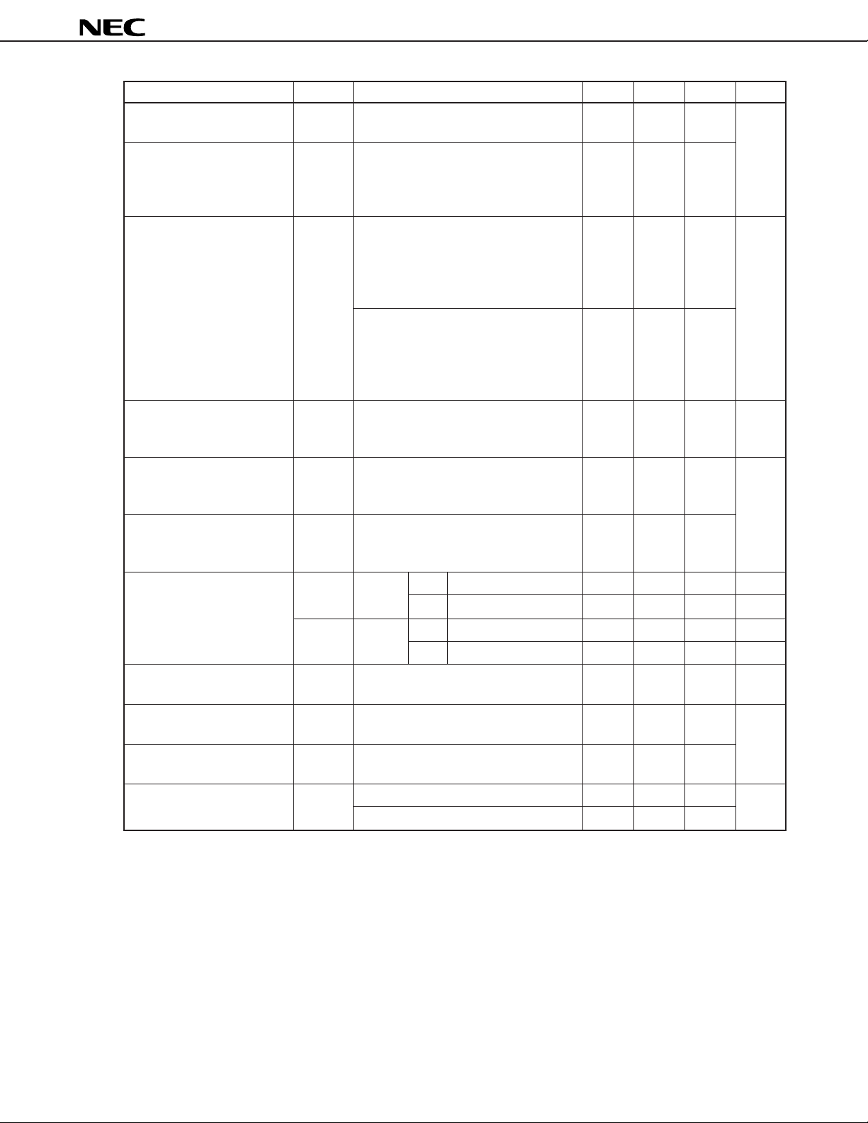
µ
PC7073
Parameter Symbol Conditions MIN. TYP. MAX. Units
Absolute delay DA A-A input signal 0 dBm0 540
characteristics
Absolute delay distortion DO A-A 500 Hz 1400
frequency characteristics 600 HZ 700
1000 to 2600 Hz 200
2800 Hz 1400
Intermodulation (2 Tone) IMD A-D input signal 44.0 dB
f1, f2: 300 to 3400 Hz
–4 to –21 dBm0
Measured signal: 2 × f1 – f2
level (2 × f1 – f2) vs level (f1, f2)
D-A input signal 44.0
f1, f2: 300 to 3400 Hz
–4 to –21 dBm0
Measured signal: 2 × f1 – f2
level (2 × f1 – f2) vs level (f1, f2)
Single frequency noise NSF D-A –54 dBm0
PAD level set at 0 dB
Measured signal up to f = 256 kHz
Deviation in gain setting ∆DGSX
for transmit channel Setting value: +7.5 to +3.0 dB –0.2 +0.2
Difference from A-D reference set value
+3.0 to –3.5 dB –0.1 +0.1
µ
dB
s
Gain setting deviation ∆DGSR
for receive chanel Setting value: 0.0 to –5.0 dB –0.1 +0.1
Idle circuit noise ICN24
ICN42
Line to ground balance LB RF = 50 Ω f = 300 to 600 Hz 42 dB
attenuation
VBB-PSRR (tone method) PSRRB IL = 20 mA f = 60 to 3400 Hz 30 dB
VCC-PSRR (tone method) PSRRC IL = 20 mA f = 60 to 3400 Hz 25
AC induction noise LFI IL = 0 mA VIN = 6 Vrms 43 dBrnc
resistance
Difference from D-A reference set value
–5.0 to –8.5 dB –0.2 +0.2
2W-4W A-law Psophometric weighted
µ
-law C message weighted
4W-2W A-law Psophometric weighted
µ
-law C message weighted
Relative accuracy = 0.5 %
IL = 20 mA VIN = 15 Vrms 20
f = 600 to 3400 Hz
f = 100 kHz –5
f = 100 kHz 5
48
–67 dBm0p
23 dBrnc0
–76 dBm0p
14 dBrnc0
13
Page 14
14
T
R
TEST0
TEST1
TEST2
TEST3
S
S
T1 R
T2
50 Ω
(0.5 %, 1 W)
Z1
Z2
50 Ω
(0.5 %, 1 W)
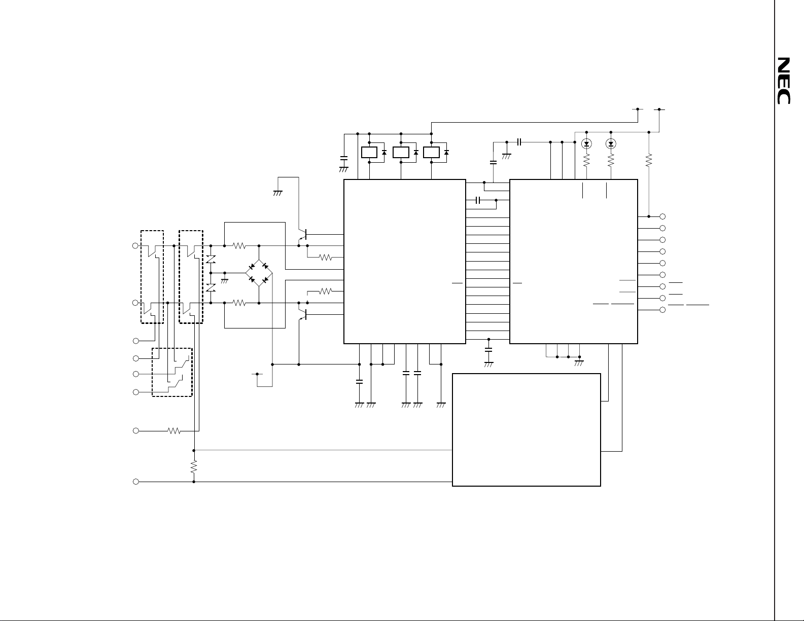
4. SYSTEM APPLICATION EXAMPLE USING
V
CC
(+5 V)
C
C
VCC
+
1 F
µ
(6 V)
37
38
R
TE
24
40
42
R
RE
32
44
45
0.1 F
(100 V)
D4
D1
Q1
3.6 kΩ (1 %, 1 W)
3.6 kΩ (1 %, 1 W)
R
FT
D2
D3
R
FR
Q4
BB
(–48 V)
V
R T1 T2
–
48 25 27 29
CC
V
RY1RY
B
T
T
E
PC7073
BB
V
47
µ
(BS-LSI)
IN
TTX
GND231GND115CPSR46C
PSR
C
0.68 F
µ
(50 V)
T
EF
T
S
R
S
R
EF
R
E
R
B
23
C
VBB
–
+
µ
2
36
–++
DC
33
C
–
0.68 F
(10 V)
3
RY
DC
DC
DC
IN+
OP
34
DC
µ
ACOM
DC
DC
BCUT
IN–
OP
T
BIAS
R
OUT3
OUT2
OUT1
IN1
IN2
ALM
PD
RC
RC
RC
BB
OUT
ASCN
AGDT
11
35
X
9
10
X
1
2
3
4
5
19
18
17
20
1
21
2
22
3
6
7
8
C
C
COM
0.1 F
µ
(5 V)
C
AC
0.68 F (50 V)
µ
+
–
GDT
–
37
38
40
39
48
47
46
45
44
30
31
32
29
28
27
43
42
41
+
0.68 F
(10 V)
VDD
+
–
0.1 F
µ
(6 V)
ACOM
ACOM
A
IN
A
OUT
CD
CD
CD
DC
DC
BCUT
11 12 13 16 15
IN
DD
OUT
AV
IN3
IN2
IN1
OUT1
PC9903
µ
OUT2
(HCS-LSI)
ALM
PD
1
RC
RC
2
RC
3
BB
IN
ASCN
AGDT
µ
AGND
SUB
36 35 34 33 26 25
DD2DVDD1
DV
DGND1
R
SUS
1 kΩ
SUS
AUX/MODE
DGND2
BSY
R
1 kΩ 2kΩ
BSY
HW
X
TYPE
FS
DCLK
HW
R
EXD
EXS
RST
IN1RTIN0
RT
23
24
22
21
20
19
18
17
14
V
DD
(+5 V)
PULL
R
HW
TYPE
FS
DCLK
HW
EXD
EXS
RST
AUX/MODE
X
R
µ
PC7073 AND
µ
PD9903
GG
CR
Ring-Trip detector
µ
PC7073
Page 15
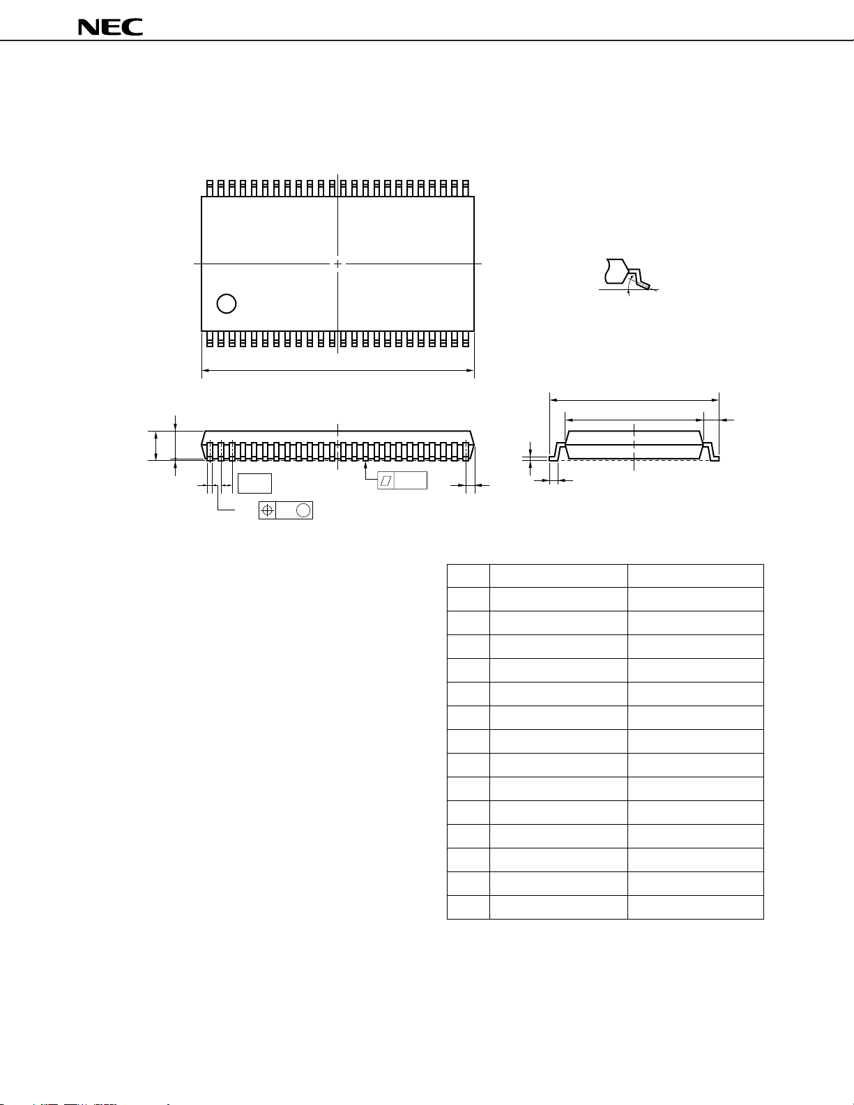
5. PACKAGE DRAWING
48 PIN PLASTIC SHRINK SOP (375 mil)
48 25
detail of lead end
–3°
+7°
3°
µ
PC7073
124
A
G
F
E
C
M
M
D
N
NOTE
Each lead centerline is located within 0.10
mm (0.004 inch) of its true position (T.P.) at
maximum material condition.
H
I
K
B
L
P48GT-65-375B-1
ITEM MILLIMETERS INCHES
0.639 MAX.
0.025 MAX.
0.026 (T.P.)
+0.004
0.012
–0.005
0.005±0.003
0.079 MAX.
0.067±0.004
+0.012
0.394
–0.013
0.315±0.008
+0.009
0.039
–0.008
+0.004
0.006
–0.002
+0.008
0.020
–0.009
0.004
0.004
M
A
B
C
D
E
F
G
H
I
J
K
L
16.21 MAX.
0.63 MAX.
0.65 (T.P.)
0.30±0.10
0.125±0.075
2.0 MAX.
1.7±0.1
10.0±0.3
8.0±0.2
1.0±0.2
+0.10
0.15
–0.05
0.5±0.2
0.10
N
0.10
J
15
Page 16
6. RECOMMENDED SOLDERING CONDITIONS
This product should be soldered and mounted under the conditions recommended below.
For details of recommended soldering conditions, refer to the information document Semiconductor Device
Mounting Technology Manual (C10535E).
For soldering methods and conditions other than those recommended, please contact your NEC sales
representative.
SURFACE MOUNT TYPE
µ
PC7073GT: 48-pin plastic shrink SOP (375 mil)
µ
PC7073
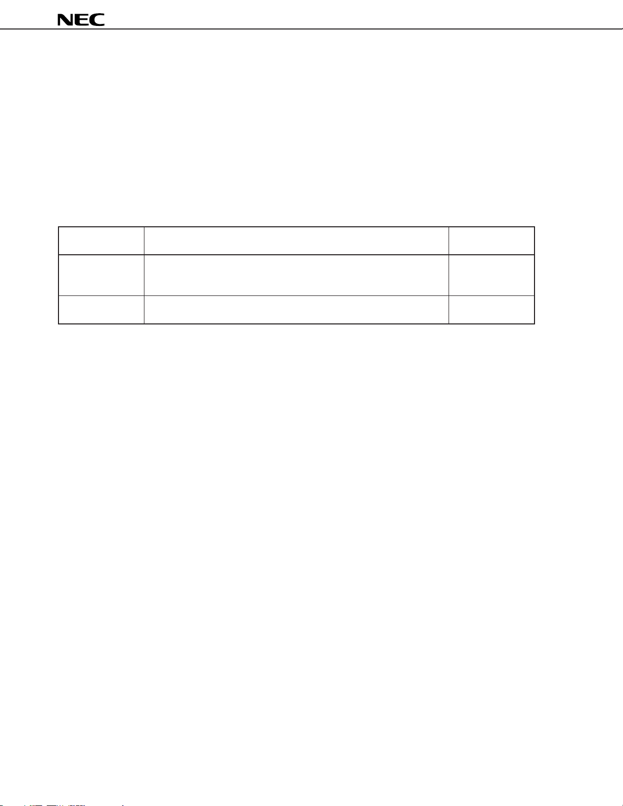
Soldering Method Soldering Conditions
Infrared reflow Package peak temperature: 235 ˚C IR35-00-1
Duration: 30 sec. max. (210 ˚C or above)
Number of times: 1
Pin heating Pin temperature: 300 ˚C max. –
Duration: 3 sec. max. (per side of device)
Note For the storage period after unpacking from the dry-pack, storage conditions are max. 25 ˚C, 65 % RH.
Recommended
Condition Symbol
16
Page 17

µ
PC7073
Notes on Handling Devices against Electrostatic Discharge
Caution When handling this device, special care against electrostatic discharge (ESD) must be taken.
If a strong ESD is applied to this device, the junction parts of the internal transistors may be
destroyed. Therefore, when transporting or storing this device, be sure to use the conductive
tray or magazine case in the packing provided by NEC, or use a conductive buffer material
or metal case. Also be sure to ground the operator's body and any tools that may enter in
contact with the device during assembly processes. Never put or leave the device on a plastic
board or table, and do not touch the device pins directly by hand.
17
Page 18

[MEMO]
µ
PC7073
18
Page 19

[MEMO]
µ
PC7073
19
Page 20

µ
PC7073
[MEMO]
The application circuits and their parameters are for reference only and are not intended for use in actual design-ins.
No part of this document may be copied or reproduced in any form or by any means without the prior written
consent of NEC Corporation. NEC Corporation assumes no responsibility for any errors which may appear in
this document.
NEC Corporation does not assume any liability for infringement of patents, copyrights or other intellectual property
rights of third parties by or arising from use of a device described herein or any other liability arising from use
of such device. No license, either express, implied or otherwise, is granted under any patents, copyrights or other
intellectual property rights of NEC Corporation or others.
While NEC Corporation has been making continuous effort to enhance the reliability of its semiconductor devices,
the possibility of defects cannot be eliminated entirely. To minimize risks of damage or injury to persons or
property arising from a defect in an NEC semiconductor device, customers must incorporate sufficient safety
measures in its design, such as redundancy, fire-containment, and anti-failure features.
NEC devices are classified into the following three quality grades:
"Standard", "Special", and "Specific". The Specific quality grade applies only to devices developed based on a
customer designated "quality assurance program" for a specific application. The recommended applications of
a device depend on its quality grade, as indicated below. Customers must check the quality grade of each device
before using it in a particular application.
Standard: Computers, office equipment, communications equipment, test and measurement equipment,
audio and visual equipment, home electronic appliances, machine tools, personal electronic
equipment and industrial robots
Special: Transportation equipment (automobiles, trains, ships, etc.), traffic control systems, anti-disaster
systems, anti-crime systems, safety equipment and medical equipment (not specifically designed
for life support)
Specific: Aircrafts, aerospace equipment, submersible repeaters, nuclear reactor control systems, life
support systems or medical equipment for life support, etc.
The quality grade of NEC devices is "Standard" unless otherwise specified in NEC's Data Sheets or Data Books.
If customers intend to use NEC devices for applications other than those specified for Standard quality grade,
they should contact an NEC sales representative in advance.
Anti-radioactive design is not implemented in this product.
M4 96.5
 Loading...