

Page 1
PRELIMINARY DATA SHEET
BIPOLAR ANALOG INTEGRATED CI RCUIT
µµµµ
PC3215TB
5 V, SUPER MINIMOLD SILICON MMIC WIDEBAND AMPLIFIER
DESCRIPTION
The µPC3215TB is a silicon monolithic IC designed as wideband amplifier. The µPC3215TB is suitable to
systems required wideband operation from HF to L band.
This IC is manufactured using NEC’s 30 GHz f
The package is 6-pin super minimold suitable for surface mount.
FEATURES
• Wideband response : fu = 2.9 GHz TYP. @3 dB bandwidth
• Noise figure : NF = 2.3 dB TYP. @f = 1.5 GHz
• Power gain : GP = 20.5 dB TYP. @f = 1.5 GHz
• Supply voltage : VCC = 4.5 to 5.5 V
• High-density surface mounting: 6-pin super minimold package
max
UHS0 (Ultra High Speed Process) silicon bipolar process.
APPLICATION
• Systems required wideband operation from HF to L band
ORDERING INFORMATION
Part Number Package Marking Supplying Form
µ
PC3215TB-E3 6-pin super minimold C3H Embossed tape 8 mm wide.
1, 2, 3 pins face the perforat i on side of the tape.
Qty 3 kpcs/reel.
Remark
To order evaluation samples, please contact your local NEC sales office. (Part number for sample
order:
PC3215TB)
µ
Caution Electro-static sensitive devices
The information in this document is subject to change without notice. Before using this document, please
confirm that this is the latest version.
Not all devices/types available in every country. Please check with local NEC representative for
availability and additional information.
Document No. P14765EJ1V0DS00 (1st edition)
Date Published April 2000 N CP(K)
Printed in Japan
©
2000
Page 2
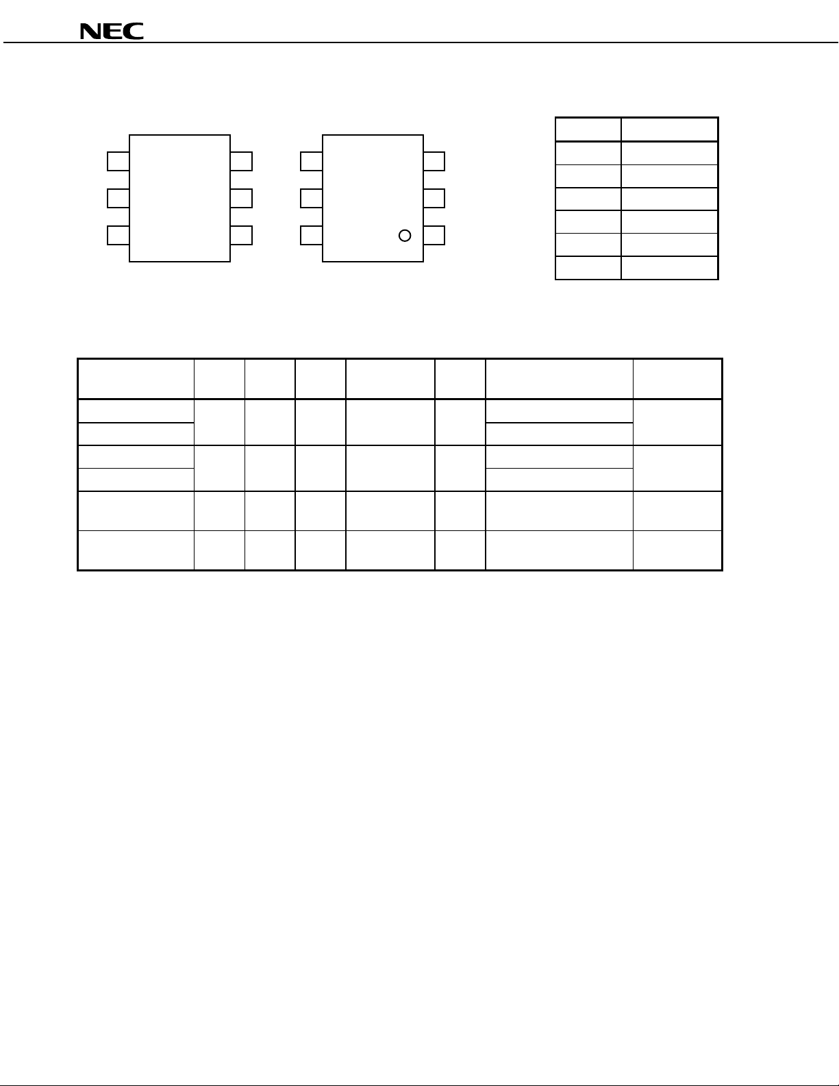
PIN CONNECTIONS
µµµµ
PC3215TB
3
2
1
(Top View)
4
5
6
C3H
(Bottom View)
4
5
6
3
2
1
PRODUCT LINE-UP OF 5V-BIAS SILICON MMIC WIDEBAND AMPLIFIERS
A
(T
= +25 °C, VCC = 5.0 V, ZS = ZL = 50
u
Part No.
PC2711T 6-pin minimold
µ
PC2711TB
µ
PC2712T 6-pin minimold
µ
PC2712TB
µ
PC3210TB 2.3 +3.5 20 3.4
µ
PC3215TB 2.9 +3.5 20.5 2.3
µ
f
(GHz)
2.9 +1.0 13 5.0
2.6 +3.0 20 4.5
O (sat)
P
(dBm)
ΩΩΩΩ
G
(dB)
)
P
NF
(dB)
@f = 1 GHz
@f = 1 GHz
@f = 1.5 GHz
@f = 1.5 GHz
CC
I
(mA)
12
6-pin super minimold
12
6-pin super minimold
15 6-pin super minimold C2X
14 6-pin super minimold C3H
Package Marking
Pin No. Pin Name
1 INPUT
2GND
3GND
4OUTPUT
5GND
6V
CC
C1G
C1H
Remark
Typical performance. Please refer to ELECTRICAL CHARACTERISTICS in detail.
Caution The package size distinguishes between minimold and super minimold.
2
Preliminary Data Sheet P14765EJ1V0DS00
Page 3
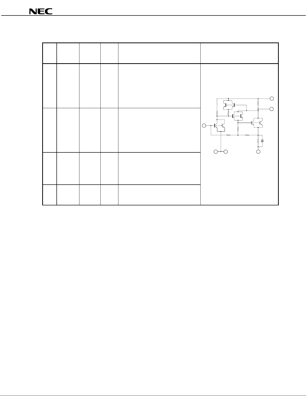
PIN EXPLANATION
µµµµ
PC3215TB
Pin
Pin Name
No.
1 INPUT
GND 0
2
Applied
Voltage
(V)
3
5
4OUTPUT
6VCC4.5 to 5.5
Pin
Voltage
Note
(V)
Function and Applications Internal Equivalent Circ ui t
0.82 Signal input pin. A internal m atching circuit,
configured with resistors, enables 50
Ω
connection over a wideband. A mul tifeedback circuit is designed to cancel the
deviations of h
FE
and resistance. This pin
must be coupled to signal source with
capacitor for DC cut.
Ground pin. This pin should be connect ed
to system ground with minimum inductance.
Ground pattern on the board should be
formed as wide as possible. All the ground
pins must be connected t ogether with wide
ground pattern to decrease impedance
difference.
3.8 Signal output pin. A internal matching
circuit, configured wi th resistors, enables 50
connection over a wideband. This pi n
Ω
must be coupled to next s tage with
capacitor for DC cut.
Power supply pin. This pin s houl d be
externally equipped with bypas s capacitor to
minimize ground impedance.
CC
V
6
4
OUT
IN
1
2
GND
5
3
GND
Pin voltage is measured at V
Note
CC
= 5.0 V
Preliminary Data Sheet P14765EJ1V0DS00
3
Page 4
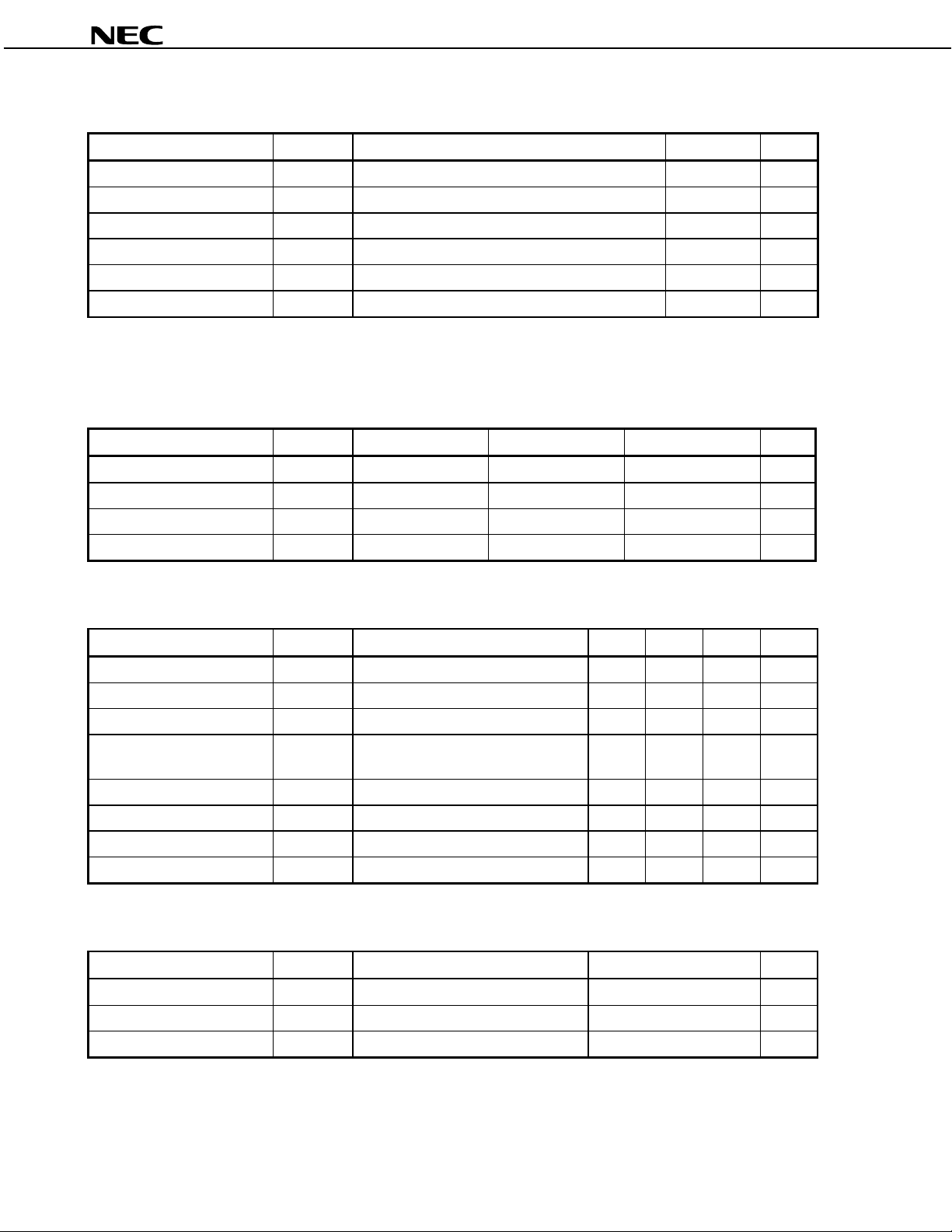
ABSOLUTE MAXIMUM RATINGS
Parameter Symbol Conditions Ratings Unit
µµµµ
PC3215TB
Supply Voltage V
Circuit Current I
Input Power P
Power Dissipation P
Operating Ambient Temperature
Storage Temperature T
Mounted on 50 × 50 × 1.6-mm epoxy glass PWB, with copper patterning on both sides.
Note
CC
CC
in
D
A
T
stg
TA = +25 °C 6.0 V
TA = +25 °C 30 mA
TA = +25 °C +10 dBm
TA = +85 °C
Note
RECOMMENDED OPERATING CONDITIONS
Parameter Symbol MIN. TYP. MAX. Unit
Supply Voltage V
Operating Ambient Temperature
Input Power
Input Frequency
CC
A
T
in
P
in
F
4.5 5.0 5.5 V
–40 +25 +85 °C
––0dBm
0.1–2.9GHz
ELECTRICAL CHARACTERISTICS (TA = +25°C, VCC = 5.0 V, ZS = ZL = 50
200 mW
–40 to +85 °C
–55 to +150 °C
)
ΩΩΩΩ
Parameter Symbol Test Conditions MIN. TYP. MAX. Unit
Circuit Current I
Power Gain G
CC
P
No input signals 10.5 14.0 17.5 mA
f = 1.5 GHz, Pin = –30 dBm 18.5 20.5 – dB
Noise Figure NF f = 1.5 GHz – 2.3 3.0 dB
Upper Limit Operating
Frequency
u
f
3 dB down below from gain at
2.5 2.9 – GHz
f = 0.1 GHz
Isolation ISL f = 1.5 GHz , Pin = –30 dBm 39 44 – dB
Input Return Loss RL
Output Return Loss RL
in
f = 1.5 GHz, Pin = –30 dBm 10 15 – dB
out
f = 1.5 GHz, Pin = –30 dBm 6.5 9.5 – dB
1 dB Compression Point P-1 –4 –1.5 – dBm
STANDARD CHARACTERISTICS (TA = +25°C, VCC = 5.0 V, ZS = ZL = 50
)
ΩΩΩΩ
Parameter Symbol Test Conditions Reference Values Unit
∆
O(sat)
G
Pin = 0 dBm +3.5 dBm
3
f1 = 1.5 GHz, f2 = 1.501 GHz +10 dBm
P
f = 0.1 to 2.15 GHz 1.0 dB
Saturated Output Power P
Output Intercept Point OIP
Gain Flatness
4
Preliminary Data Sheet P14765EJ1V0DS00
Page 5
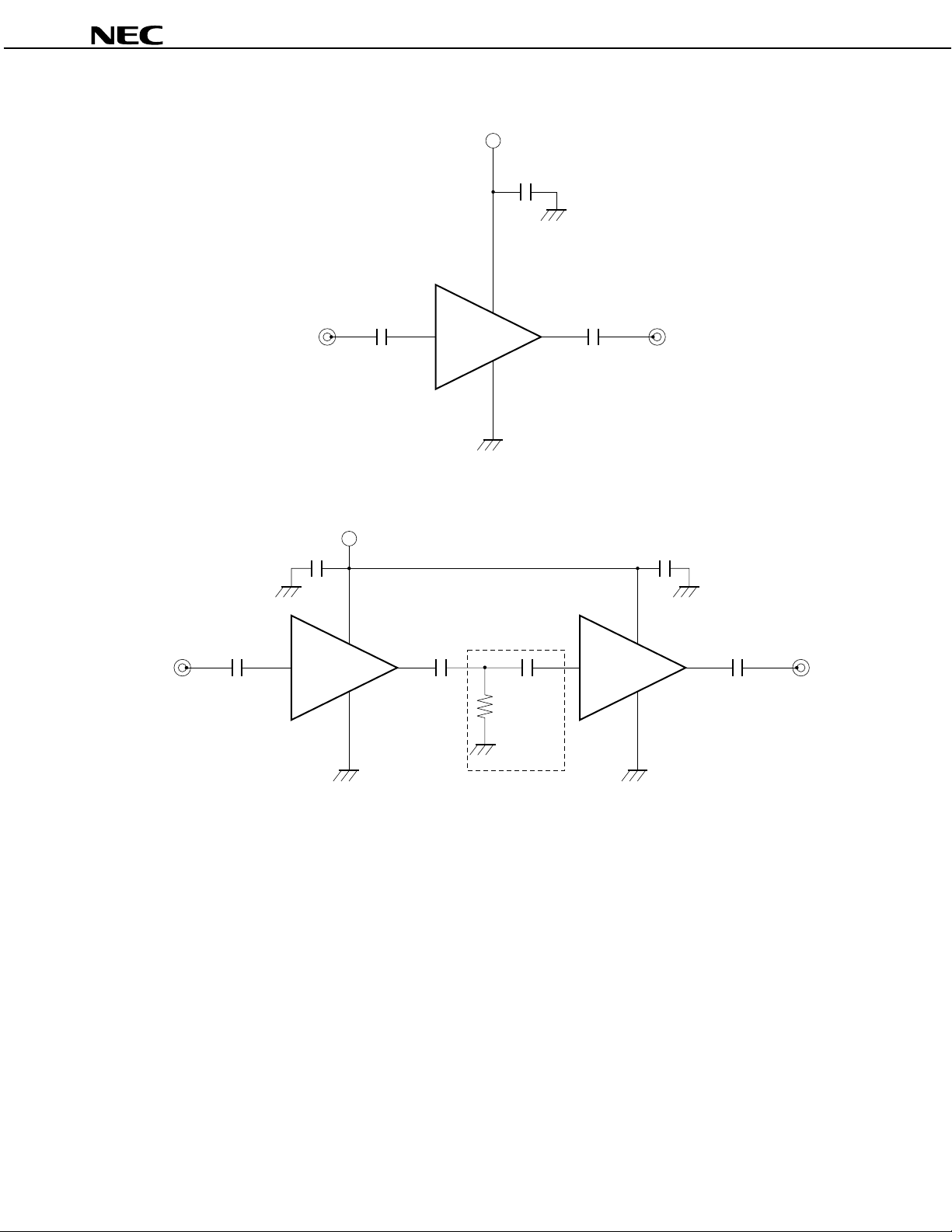
TEST CIRCUIT
6
V
CC
1 000 pF
C
3
µµµµ
PC3215TB
50 Ω
IN
C
1
1 000 pF
EXAMPLE OF APPLICATION CIRCUIT
CC
V
1 000 pF
6
50 Ω
IN
1 000 pF 1 000 pF
1
4
2, 3, 5
1
1 000 pF
4
2, 3, 5
50 to 200 Ω
2
C
1 000 pF
1
50 Ω
1 000 pF
6
2, 3, 5
OUT
4
50 Ω
OUT
1 000 pF
Please connect these
component to stabilize
operation.
The application circuits and their parameters are for reference only and are not intended for use in actual design-ins.
Capacitors for VCC, input and output pins
CC
1 000 pF capacitors are recommendable as bypass capacitor for V
pin and coupling capacitors for input/output
pins.
Bypass capacitor for VCC pin is intended to minimize VCC pin’s ground impedance. Therefore, stable bias can be
supplied against VCC fluctuation.
Coupling capacitors for input/output pins are intended to minimize RF serial impedance and cut DC.
To get flat gain from 100 MHz up, 1 000 pF capacitors are assembled on the test circuit. [Actually, 1 000 pF
capacitors give flat gain at least 10 MHz. In the case of under 10 MHz operation, increase the value of coupling
capacitor such as 2 200 pF. Because the coupling capacitors are determined by the equation of C = 1/(2 π fZs).]
Preliminary Data Sheet P14765EJ1V0DS00
5
Page 6
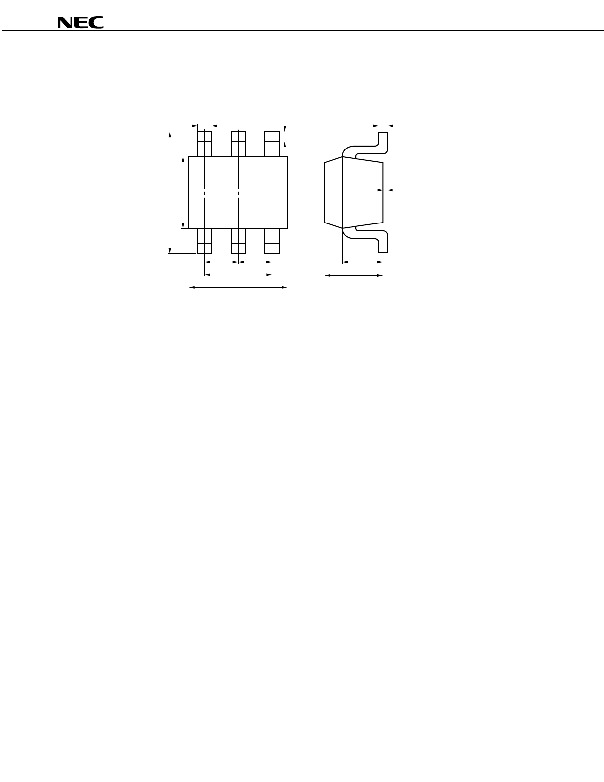
PACKAGE DIMENSIONS
6 PIN SUPER MINIMOLD (UNIT: mm)
µµµµ
PC3215TB
2.1 ±0.1
1.25 ±0.1
0.2
+0.1
–0.05
0.65 0.65
1.3
2.0 ±0.2
0.1 MIN.
0.7
0.9 ±0.1
0.15
+0.1
–0.05
0 to 0.1
6
Preliminary Data Sheet P14765EJ1V0DS00
Page 7

µµµµ
PC3215TB
NOTES ON CORRECT USE
(1) Observe precautions for handling because of electro-static sensitive devices.
(2) Form a ground pattern as widely as possible to minimize ground impedance (to prevent undesired oscillation).
(3) Keep the track length of the ground pins as short as possible.
(4) A low pass filter must be attached to VCC line.
RECOMMENDED SOLDERING CONDITIONS
This product should be soldered under the following recommended conditions. For soldering methods and
conditions other than those recommended below, contact your NEC sales representative.
Soldering Method Soldering Conditions Recommended Condition Symbol
Infrared Reflow Package peak temperature: 235 °C or below
Time: 30 seconds or less (at 210 °C)
Count: 3, Exposure limi t: None
VPS Package peak temperature: 215 ° C or bel ow
Time: 40 seconds or less (at 200 °C)
Count: 3, Exposure limi t: None
Wave Soldering Soldering bath temperature: 260 °C or bel ow
Time: 10 seconds or less
Count: 1, Exposure limi t: None
Partial Heating Pin temperature: 300 °C
Time: 3 seconds or less (per side of device)
Exposure limit: None
After opening the dry pack, keep it in a place below 25 °C and 65 % RH for the allowable storage period.
Note
Note
Note
Note
Note
IR35-00-3
VP15-00-3
WS60-00-1
–
Caution Do not use different soldering methods together (except for partial heating).
For details of recommended soldering conditions for surface mounting, refer to information document
SEMICONDUCTOR DEVICE MOUNTING TECHNOLOGY MANUAL (C10535E).
Preliminary Data Sheet P14765EJ1V0DS00
7
Page 8

µµµµ
PC3215TB
• The information in this document is subject to change without notice. Before using this document, please
confirm that this is the latest version.
• No part of this document may be copied or reproduced in any form or by any means without the prior written
consent of NEC Corporation. NEC Corporation assumes no responsibility for any errors which may appear in
this document.
• NEC Corporation does not assume any liability for infringement of patents, copyrights or other intellectual property
rights of third parties by or arising from use of a device described herein or any other liability arising from use
of such device. No license, either express, implied or otherwise, is granted under any patents, copyrights or other
intellectual property rights of NEC Corporation or others.
• Descriptions of circuits, software, and other related information in this document are provided for illustrative
purposes in semiconductor product operation and application examples. The incorporation of these circuits,
software, and information in the design of the customer's equipment shall be done under the full responsibility
of the customer. NEC Corporation assumes no responsibility for any losses incurred by the customer or third
parties arising from the use of these circuits, software, and information.
• While NEC Corporation has been making continuous effort to enhance the reliability of its semiconductor devices,
the possibility of defects cannot be eliminated entirely. To minimize risks of damage or injury to persons or
property arising from a defect in an NEC semiconductor device, customers must incorporate sufficient safety
measures in its design, such as redundancy, fire-containment, and anti-failure features.
• NEC devices are classified into the following three quality grades:
"Standard", "Special", and "Specific". The Specific quality grade applies only to devices developed based on a
customer designated "quality assurance program" for a specific application. The recommended applications of
a device depend on its quality grade, as indicated below. Customers must check the quality grade of each device
before using it in a particular application.
Standard: Computers, office equipment, communications equipment, test and measurement equipment,
audio and visual equipment, home electronic appliances, machine tools, personal electronic
equipment and industrial robots
Special: Transportation equipment (automobiles, trains, ships, etc.), traffic control systems, anti-disaster
systems, anti-crime systems, safety equipment and medical equipment (not specifically designed
for life support)
Specific: Aircraft, aerospace equipment, submersible repeaters, nuclear reactor control systems, life
support systems or medical equipment for life support, etc.
The quality grade of NEC devices is "Standard" unless otherwise specified in NEC's Data Sheets or Data Books.
If customers intend to use NEC devices for applications other than those specified for Standard quality grade,
they should contact an NEC sales representative in advance.
M7 98. 8
 Loading...