

Page 1
DATA SHEET
BIPOLAR ANALOG INTEGRATED CI RCUIT
µµµµ
PC3210TB
5 V, SUPER MINIMOLD SILICON MMIC WIDEBAND AMPLIFIER
DESCRIPTION
The µPC3210TB is a silicon monolithic integrated circuits designed as wideband amplifier. The µPC3210TB is
suitable to systems required wideband operation from HF to L band.
This IC is manufactured using NEC’s 20 GHz fT NESAT™III silicon bipolar process. This process uses silicon
nitride passivation film and gold electrodes. These materials can protect chip surface from external pollution and
prevent corrosion/migration. Thus, this IC has excellent performance, uniformity and reliability.
FEATURES
• High-density surface mounting: 6-pin super minimold package
• Supply voltage : VCC = 4.5 to 5.5 V
• Wideband response : fu = 2.3 GHz TYP. @3 dB bandwidth
• Power gain : GP = 20 dB TYP. @f = 1.5 GHz
• Noise figure : NF = 3.4 dB TYP. @f = 1.5 GHz
APPLICATION
• Systems required wideband operation from HF to 2.0 GHz
ORDERING INFORMATION
Part Number Package Marking Supplying Form
µ
PC3210TB-E3 6-pin super minimold C2X Embossed tape 8 mm wide.
1, 2, 3 pins face to perforat i on side of the tape.
Qty 3 kp/reel.
Remark
To order evaluation samples, please contact your local NEC sales office. (Part number for sample
order:
PC3210TB)
µ
Caution Electro-static sensitive devices
The information in this document is subject to change without notice. Before using this document, please
confirm that this is the latest version.
Not all devices/types available in every country. Please check with local NEC representative for
availability and additional information.
Document No. P13593EJ2V0DS00 (2nd edition)
Date Published May 1999 N CP(K)
Printed in Japan
The mark shows major revised points.
©
1998, 1999
Page 2
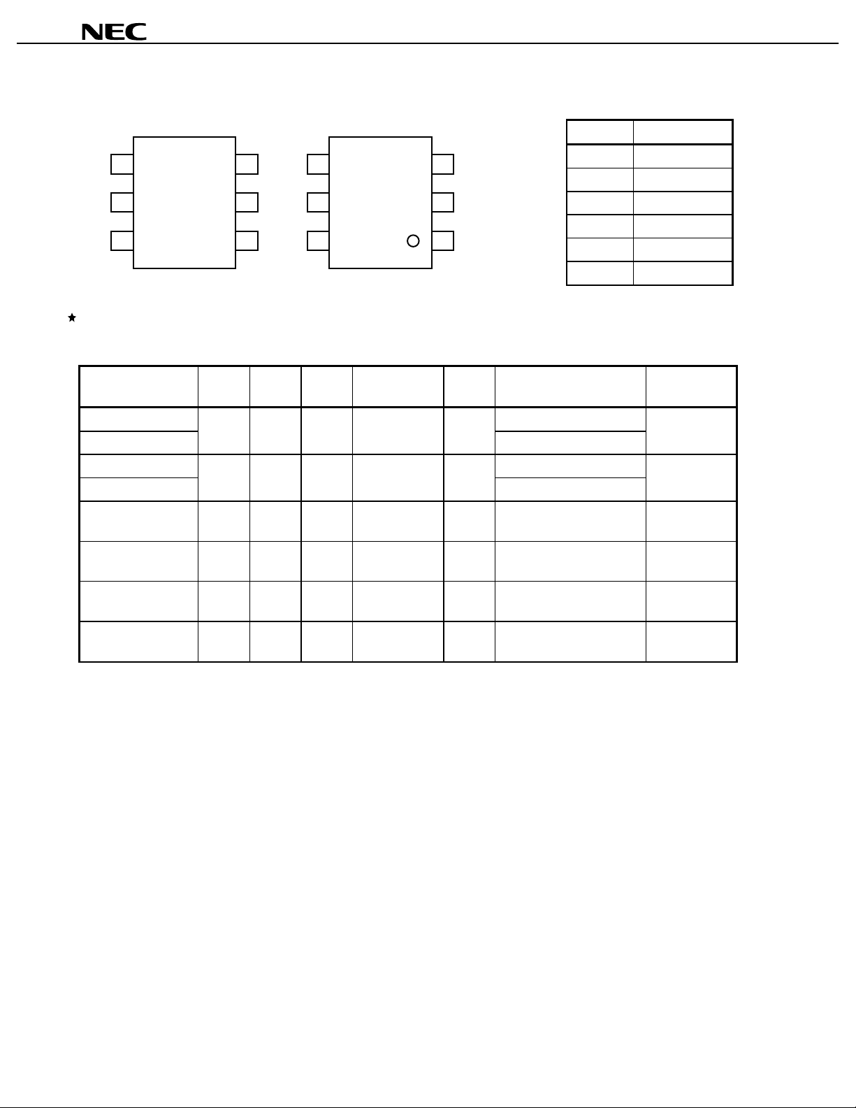
PIN CONNECTIONS
µµµµ
PC3210TB
3
2
1
(Top View)
4
5
6
C2X
(Bottom View)
4
5
6
3
2
1
PRODUCT LINE-UP OF 5V-BIAS SILICON MMIC WIDEBAND AMPLIFIERS
A
= +25 °C, VCC = 5.0 V, ZL = ZS = 50
(T
u
Part No.
PC2711T 6-pin minimold
µ
PC2711TB
µ
PC2712T 6-pin minimold
µ
PC2712TB
µ
PC2713T 1.2 +7.0 29 3.2
µ
PC2791TB 1.9 +4.0 12 5.5
µ
PC2792TB 1.2 +5.0 20 3.5
µ
PC3210TB 2.3 +3.5 20 3.4
µ
f
(GHz)
2.9 +1.0 13 5.0
2.6 +3.0 20 4.5
O (sat)
P
(dBm)
ΩΩΩΩ
G
(dB)
)
P
NF
(dB)
@f = 1 GHz
@f = 1 GHz
@f = 0.5 GHz
@f = 0.5 GHz
@f = 0.5 GHz
@f = 1.5 GHz
CC
I
(mA)
12
6-pin super minimold
12
6-pin super minimold
12 6-pin minimold C1J
17 6-pin super minimold C2S
19 6-pin super minimold C2T
15 6-pin super minimold C2X
Package Marking
Pin No. Pin Name
1 INPUT
2GND
3GND
4OUTPUT
5GND
6V
CC
C1G
C1H
Remark
Notice
2
Typical performance. Please refer to ELECTRICAL CHARACTERISTICS in detail.
The package size distinguishes between minimold and super minimold.
Data Sheet P13593EJ2V0DS00
Page 3
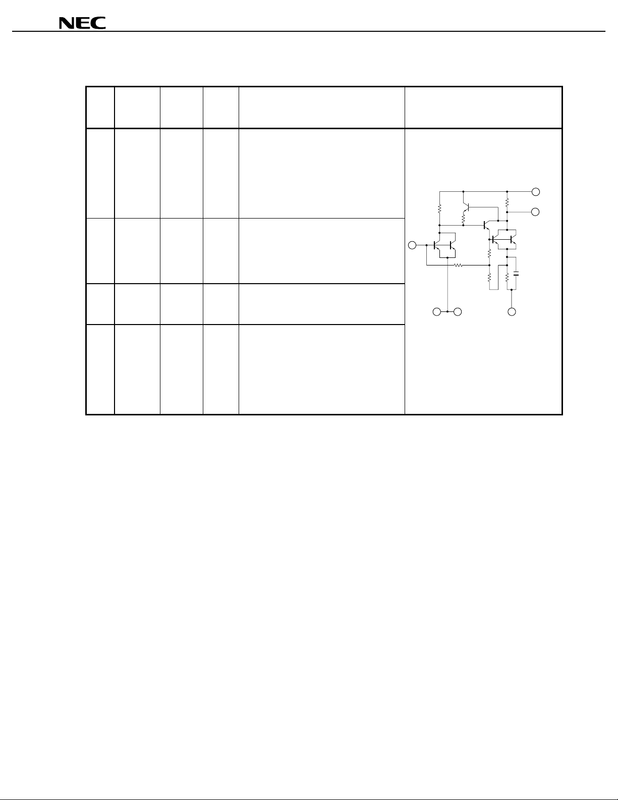
PIN EXPLANATION
µµµµ
PC3210TB
Pin
Pin Name
No.
1 INPUT
4OUTPUT
Applied
Voltage
V
6VCC4.5 to 5.5
2
GND 0
3
5
Pin
Voltage
Note
V
Function and Applications Internal Equivalent Circ ui t
0.82 Signal input pin. A internal m atching circuit,
configured with resistors, enables 50
Ω
connection over a wide band. A mul tifeedback circuit is designed to cancel the
FE
deviations of h
and resistance. This pin
must be coupled to signal source with
capacitor for DC cut.
4.0 Signal output pin. A internal matching
circuit, configured wi th resistors, enables 50
connection over a wide band. This pi n
Ω
must be coupled to next s tage with
capacitor for DC cut.
Power supply pin. This pin s houl d be
externally equipped with bypas s capacitor to
minimize ground impedance.
Ground pin. This pin should be connect ed
to system ground with minimum inductance.
Ground pattern on the board should be
formed as wide as possible. All the ground
pins must be connected t ogether with wide
ground pattern to decrease impedance
difference.
1
IN
2
GND GND
V
CC
6
4
OUT
5
3
Pin voltage is measured at V
Note
CC
= 5.0 V
Data Sheet P13593EJ2V0DS00
3
Page 4
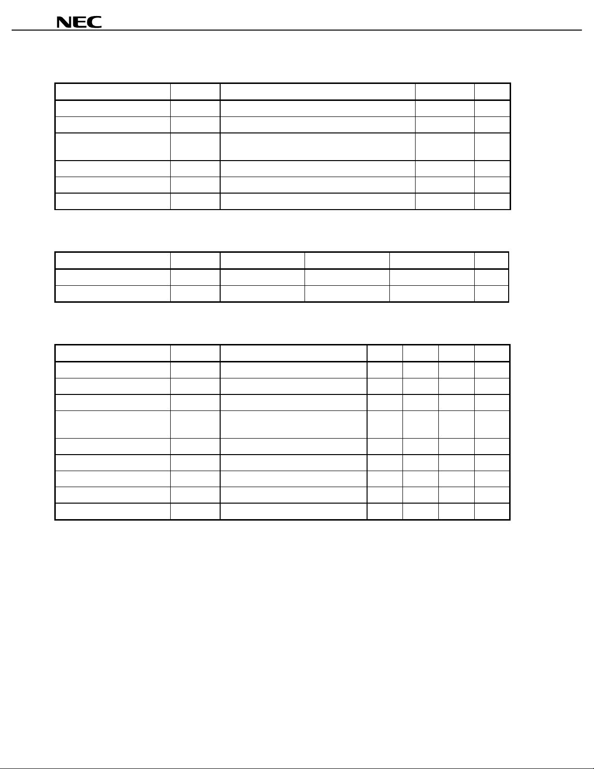
ABSOLUTE MAXIMUM RATINGS
Parameter Symbol Conditions Ratings Unit
µµµµ
PC3210TB
Supply Voltage V
Circuit Current I
Total Power Dissipat i on P
Operating Ambient Temperature
Storage Temperature T
Input Power Level P
CC
CC
D
A
T
stg
in
TA = +25 °C 6.0 V
TA = +25 °C 30 mA
Mounted on double sided copper clad
50 × 50 × 1.6 mm epoxy glass P WB (T
A
= +85 °C)
200 mW
–40 to +85 °C
–55 to +150 °C
TA = +25 °C +10 dBm
RECOMMENDED OPERATING CONDITIONS
Parameter Symbol MIN. TYP. MAX. Unit
T
CC
f
O (sat)
G
∆
CC
A
4.5 5.0 5.5 V
–40 +25 +85 °C
)
ΩΩΩΩ
No signals 11.5 15.0 19.5 mA
P
u
f = 1.5 GHz 18 20 – dB
3 dB down below from gain at
2.05 2.3 – GHz
f = 0.1 GHz
in
f = 1.5 GHz 10 14.5 – dB
out
f = 1.5 GHz 7 11 – dB
f = 1.5 GHz, Pin = 0 dBm +0.5 +3.5 – dBm
P
f = 0.1 GHz to 2.05 GHz –
1.0 – dB
±
Supply Voltage V
Operating Ambient Temperature
ELECTRICAL OPERATING CONDITIONS (TA = +25°C, VCC = 5.0 V, ZS = ZL = 50
Parameter Symbol Test Conditions MIN. TYP. MAX. Unit
Circuit Current I
Power Gain G
Noise Figure NF f = 1.5 GHz – 3.4 4.4 dB
Upper Limit Operating
Frequency
Isolation ISL f = 1.5 GHz 29 34 – dB
Input Return Loss RL
Output Return Loss RL
Maximum Output Level P
Gain Flatness
4
Data Sheet P13593EJ2V0DS00
Page 5
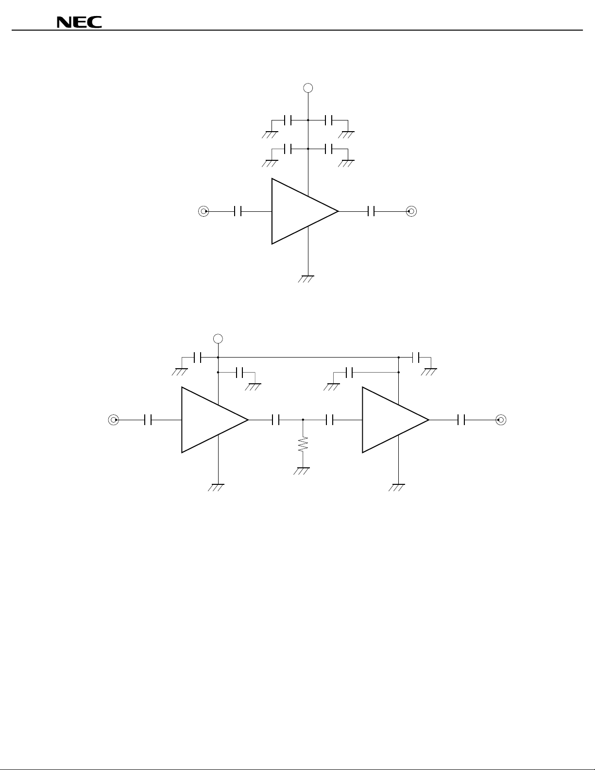
TEST CIRCUIT
V
CC
1 000 pF 1 000 pF
C
4
C
3
C
6
C
5
1 000 pF 1 000 pF
6
µµµµ
PC3210TB
50 Ω
1
C
IN
1 000 pF
EXAMPLE OF APPLICATION CIRCUIT
V
CC
1 000 pF
C
4
IN
C
3
6
50 Ω
1
C
1
1 000 pF 1 000 pF
2, 3, 5
1
4
1 000 pF
C
1 000 pF
2
C
4
50 Ω
OUT
1 000 pF
2, 3, 5
1 000 pF
C
1 000 pF
5
C
6
6
7
8
C
1
C
4
50 Ω
2
OUT
1 000 pF
R
1
50 to 200 Ω
To stabilize operation,
please connect R
1
, C
2, 3, 5
8
The application circuits and their parameters are for reference only and are not intended for use in actual design-ins.
Capacitors for VCC, input and output pins
CC
1 000 pF capacitors are recommendable as bypass capacitor for V
pin and coupling capacitors for input/output
pins.
Bypass capacitor for VCC pin is intended to minimize VCC pin’s ground impedance. Therefore, stable bias can be
supplied against VCC fluctuation.
Coupling capacitors for input/output pins are intended to minimize RF serial impedance and cut DC.
To get flat gain from 100 MHz up, 1 000 pF capacitors are assembled on the test circuit. [Actually, 1 000 pF
capacitors give flat gain at least 10 MHz. In the case of under 10 MHz operation, increase the value of coupling
capacitor such as 2 200 pF. Because the coupling capacitors are determined by the equation of C = 1/(2 π fZs).]
Data Sheet P13593EJ2V0DS00
5
Page 6

ILLUSTRATION OF THE TEST CIRCUIT ASSEMBLED ON EVALUATION BOARD
Top View
OUT
C2X
Mounting Direction
IN
C1
C3
C4
C5
C2
C6
µµµµ
PC3210TB
COMPONENT LIST
C1 to C6 1 000 pF
Value
Notes
1. 42 × 35 × 0.4 mm double sided copper clad polyimide board.
2. Back side: GND pattern
3. Solder plated on pattern
4.
: Through holes
6
Data Sheet P13593EJ2V0DS00
Page 7
µµµµ
PC3210TB
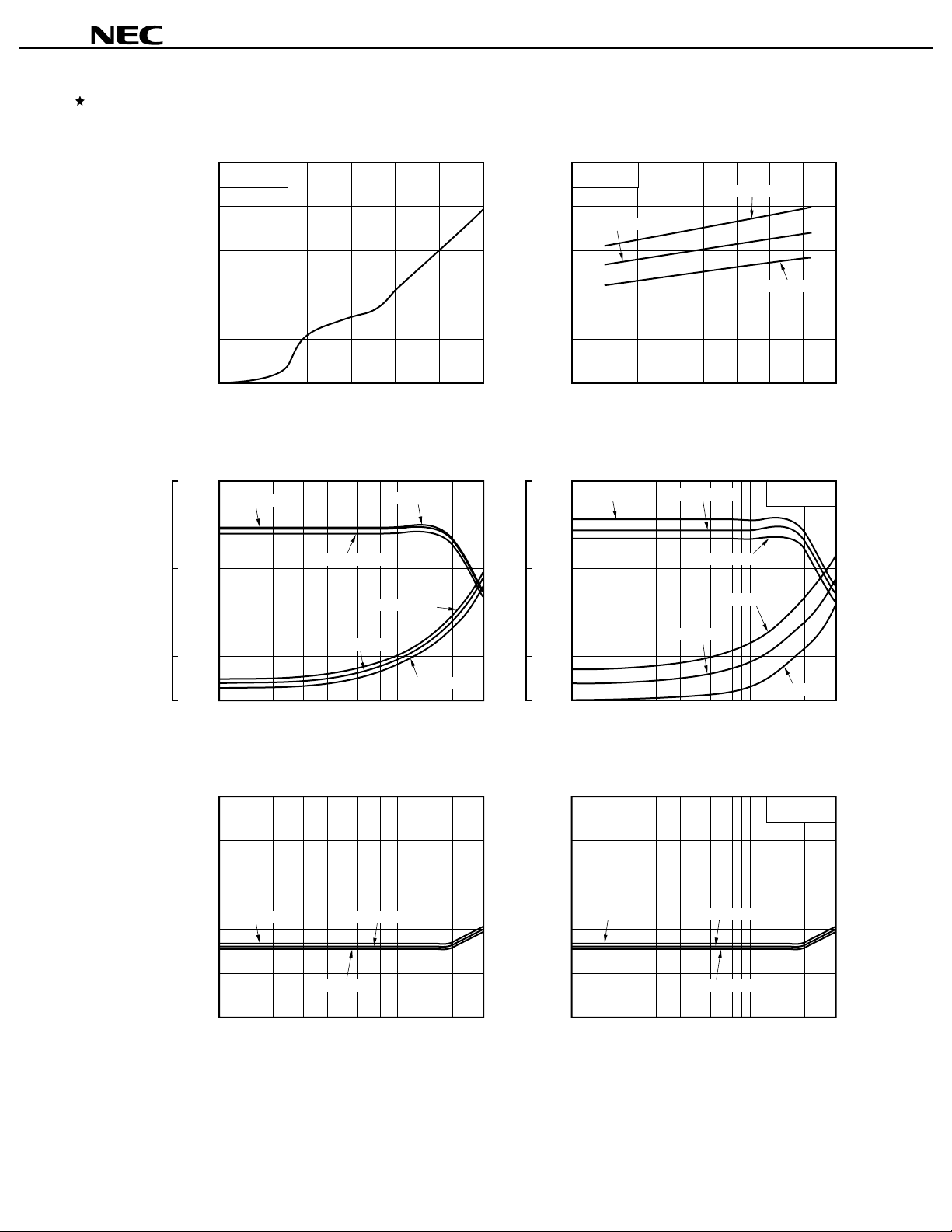
TYPICAL CHARACTERISTICS (Unless otherwise specified, TA = +25
CIRCUIT CURRENT vs. SUPPLY VOLTAGE
25
No input signal
20
(mA)
CC
15
10
Circuit Current I
5
0
0123456
CC
Supply Voltage V
(V)
NOISE FIGURE AND INSERTION POWER GAIN vs. FREQUENCY NOISE FIGURE AND INSERTION POWER GAIN vs. FREQUENCY
25
7
VCC = 5.0 V
20
6
(dB)
P
G
P
15
5
VCC = 4.5 V
VCC = 5.5 V
CIRCUIT CURRENT vs. OPERATING AMBIENT TEMPERATURE
25
No input signal
20
VCC = 5.0 V
(mA)
CC
15
10
Circuit Current I
5
0
−60 −40 −20 0 +20 +40 +60 +80 +
Operating Ambient Temperature T
25
7
TA = −40 °C
20
6
(dB)
P
15
5
C)
°°°°
G
P
VCC = 5.5 V
TA = +25 °C
TA = +85 °C
VCC = 4.5 V
A
(°C)
VCC = 5.0 V
100
10
4
Noise Figure NF (dB)
5
3
Insertion Power Gain G
0
2
0.1 0.3 1.0 3.0
0
−10
−20
VCC = 5.5 V VCC = 5.0 V
−30
Isolation ISL (dB)
−40
−50
0.1 0.3 1.0 3.0
VCC = 5.5 V
NF
VCC = 5.0 V
VCC = 4.5 V
Frequency f (GHz)
ISOLATION vs. FREQUENCY
VCC = 4.5 V
Frequency f (GHz)
10
4
Noise Figure NF (dB)
3
2
5
Insertion Power Gain G
0
0.1 0.3 1.0 3.0
0
−10
−20
TA = +85 °C
−30
Isolation ISL (dB)
−40
−50
0.1 0.3 1.0 3.0
TA = +85 °C
TA = +25 °C
NF
TA = −40 °C
Frequency f (GHz)
ISOLATION vs. FREQUENCY
VCC = 5.0 V
TA = +25 °C
TA = −40 °C
Frequency f (GHz)
Data Sheet P13593EJ2V0DS00
7
Page 8

µµµµ
PC3210TB
INPUT RETURN LOSS vs. FREQUENCY
0
VCC = 5.5 V
VCC = 5.0 V
VCC = 4.5 V
Input Return Loss RLin (dB)
0.1 0.3 1.0
Frequency f (GHz)
OUTPUT RETURN LOSS vs. FREQUENCY OUTPUT RETURN LOSS vs. FREQUENCY
0
VCC = 5.5 V
VCC = 5.0 V
3.0
−10
−15
−20
Input Return Loss RLin (dB)
−25
−10
−5
−5
INPUT RETURN LOSS vs. FREQUENCY
0
−5
−10
TA = −40 °C
−15
−20
−25
0.1 0.3 1.0
0
−5
TA = +25 °C TA = −40 °C
−10
TA = +85 °C
Frequency f (GHz)
VCC = 5.0 V
TA = +25 °C
3.0
VCC = 5.0 V
−15
−20
Output Return Loss RLout (dB)
−25
0.1 0.3 1.0 3.0
OUTPUT POWER vs. INPUT POWER
+10
f = 1.0 GHz
+5
0
−5
−10
−15
−20
Output Power Pout (dBm)
−25
−30
−
40−35−30−25−20−15−10−5
VCC = 4.5 V
Frequency f (GHz)
VCC = 5.5 V
VCC = 4.5 V
Input Power P
in (dBm)
VCC = 5.0 V
+5+
−15
TA = +85 °C
−20
Output Return Loss RLout (dB)
−25
0.1 0.3 1.0 3.0
Frequency f (GHz)
OUTPUT POWER vs. INPUT POWER
+10
f = 1.0 GHz
CC = 5.0 V
V
+5
0
−5
−10
−15
−20
Output Power Pout (dBm)
−25
−30
100
−
TA = +85 °C
40−35−30−25−20−15−10−5
TA = −40 °C
TA = +25 °C
Input Power P
in (dBm)
+5+
100
8
Data Sheet P13593EJ2V0DS00
Page 9

µµµµ
PC3210TB
OUTPUT POWER vs. INPUT POWER
+10
f = 1.5 GHz
+5
0
(dBm)
−5
out
−10
VCC = 4.5 V
−15
−20
Output Power P
−25
−30
−
40−35−30−25−20−15−10−5
Input Power P
OUTPUT POWER vs. INPUT POWER
+10
f = 2.0 GHz
+5
VCC = 5.5 V
0
(dBm)
−5
out
−10
VCC = 4.5 V
−15
−20
Output Power P
−25
−30
−
40−35−30−25−20−15−10−5
Input Power P
VCC = 5.5 V
VCC = 5.0 V
in
(dBm)
VCC = 5.0 V
in
(dBm)
+5+
+5+
OUTPUT POWER vs. INPUT POWER
+10
f = 1.5 GHz
CC
= 5.0 V
V
+5
0
(dBm)
−5
out
TA = −40 °C
TA = +25 °C
−10
−15
−20
Output Power P
TA = +85 °C
−25
−30
100
−
40−35−30−25−20−15−10−5
in
Input Power P
(dBm)
+5+
100
OUTPUT POWER vs. INPUT POWER
+10
f = 2.0 GHz
CC
= 5.0 V
V
+5
0
TA = −40 °C
(dBm)
−5
out
TA = +25 °C
−10
−15
−20
Output Power P
TA = +85 °C
−25
−30
−
100
40−35−30−25−20−15−10−5
in
Input Power P
(dBm)
+5+
100
SATURATED OUTPUT POWER vs. FREQUENCY
+10
VCC = 5.5 V
Pin = 0 dBm
(dBm)
+5
O (sat)
VCC = 4.5 V
VCC = 5.0 V
0
−5
Saturated Output Power P
−10
0.1 0.3 1.0 3.0
Frequency f (GHz)
SATURATED OUTPUT POWER vs. FREQUENCY
+10
TA = +85 °C
VCC = 5.0 V
in
P
(dBm)
+5
O (sat)
TA = −40 °C
TA = +25 °C
0
−5
Saturated Output Power P
−10
0.1 0.3 1.0 3.0
Frequency f (GHz)
= 0 dBm
Data Sheet P13593EJ2V0DS00
9
Page 10

µµµµ
PC3210TB
THIRD ORDER INTERMODULATION DISTORTION
AND OUTPUT POWER OF EACH TONE vs.
INPUT POWER OF EACH TONE
f1 = 1 000 MHz
f
2
= 1 002 MHz
P
out (each)
VCC = 4.5 V
IM
3
VCC = 5.5 V
VCC = 5.0 V
VCC = 5.5 V
VCC = 5.0 V
VCC = 4.5 V
(dBm)
3
(dBm)
out (each)
+10
0
−10
−20
−30
−40
−50
−60
Output Power of Each Tone P
−40 −35 −30 −25 −20 −15 −10 −5
3rd Order Intermodulation Distortion IM
Input Power of Each Tone P
in (each)
THIRD ORDER INTERMODULATION DISTORTION
AND OUTPUT POWER OF EACH TONE vs.
INPUT POWER OF EACH TONE
f1 = 1 500 MHz
2
= 1 502 MHz
f
P
out (each)
VCC = 4.5 V
VCC = 5.5 V
VCC = 5.0 V
VCC = 5.5 V
VCC = 5.0 V
(dBm)
3
(dBm)
out (each)
+10
0
−10
−20
−30
VCC = 4.5 V
IM
−40
3
−50
−60
Output Power of Each Tone P
3rd Order Intermodulation Distortion IM
Input Power of Each Tone P
in (each)
THIRD ORDER INTERMODULATION DISTORTION
AND OUTPUT POWER OF EACH TONE vs.
+10
(dBm)
3
(dBm)
0
out (each)
−10
−20
−30
−40
−50
−60
Output Power of Each Tone P
−40 −35 −30 −25 −20 −15 −10 −50
3rd Order Intermodulation Distortion IM
INPUT POWER OF EACH TONE
f
1
= 2 000 MHz
2
= 2 002 MHz
f
P
out (each)
VCC = 4.5 V
IM
3
VCC = 4.5 V
Input Power of Each Tone P
VCC = 5.5 V
VCC = 5.0 V
VCC = 5.5 V
VCC = 5.0 V
in (each)
(dBm)
(dBm)
(dBm)
THIRD ORDER INTERMODULATION DISTORTION
−50
(dBc)
3
−45
−40
−35
−30
vs. OUTPUT POWER OF EACH TONE
f
1
= 1 000 MHz
f
2
= 1 002 MHz
VCC = 4.5 V
VCC = 5.5 V
VCC = 5.0 V
−25
−20
−15
−10
−5
0
0
−20 −15 −10 −50
3rd Order Intermodulation Distortion IM
Output Power of Each Tone P
out (each)
(dBm)
THIRD ORDER INTERMODULATION DISTORTION
−50
(dBc)
3
−45
−40
−35
−30
−25
vs. OUTPUT POWER OF EACH TONE
f
1
= 1 500 MHz
2
= 1 502 MHz
f
VCC = 5.5 V
VCC = 5.0 V
VCC = 4.5 V
−20
−15
−10
−5
0
0−40 −35 −30 −25 −20 −15 −10 −5
−20 −15 −10 −50
3rd Order Intermodulation Distortion IM
out (each)
Output Power of Each Tone P
(dBm)
THIRD ORDER INTERMODULATION DISTORTION
−50
(dBc)
3
−45
vs. OUTPUT POWER OF EACH TONE
f1 = 2 000 MHz
2
= 2 002 MHz
f
−40
−35
−30
−25
VCC = 5.5 V
−20
−15
−10
−5
0
−20 −15 −10 −50
3rd Order Intermodulation Distortion IM
Output Power of Each Tone P
VCC = 5.0 V
VCC = 4.5 V
out (each)
(dBm)
10
Data Sheet P13593EJ2V0DS00
Page 11

S-PARAMETER (VCC = 5.0 V)
11
S
FREQUENCY
−−−−
0.1 G
1 G
2.0 G
µµµµ
PC3210TB
22
S
FREQUENCY
−−−−
2.0 G
0.1 G
1.0 G
Data Sheet P13593EJ2V0DS00
11
Page 12

µµµµ
PC3210TB
TYPICAL S-PARAMETER VALUES (TA = +25
PC3210TB
µ
C)
°°°°
VCC = 5.0 V, ICC = 16 mA
FREQUENCY S
MHz MAG. ANG. MAG. ANG. MAG. ANG. MAG. ANG.
100.0000 0.358 171.9 8.688
200.0000 0.335 166.6 8.807
300.0000 0.321 160.7 8.821
400.0000 0.306 158.3 8.841
500.0000 0.294 154.4 8.908
600.0000 0.283 151.8 8.990
700.0000 0.273 148.6 9.160
800.0000 0.267 146.0 9.342
900.0000 0.260 144.2 9.541
1000.0000 0.252 141.5 9.741
1100.0000 0.246 138.4 10.071
1200.0000 0.239 135.9 10.393
1300.0000 0.229 133.3 10.513
1400.0000 0.224 131.1 10.763
1500.0000 0.215 127.4 10.708
1600.0000 0.203 125.8 10.720
1700.0000 0.191 123.1 10.388
1800.0000 0.179 122.1 9.993
1900.0000 0.163 121.0 9.507
2000.0000 0.155 123.4 8.983
2100.0000 0.140 126.1 8.384
2200.0000 0.133 129.1 7.905
2300.0000 0.130 135.3 7.412
2400.0000 0.133 139.0 6.976
2500.0000 0.137 144.0 6.582 176.1 0.038 73.2 0.157
2600.0000 0.149 148.5 6.202 170.4 0.039 71.4 0.136
2700.0000 0.157 150.2 5.942 164.9 0.043 73.7 0.116
2800.0000 0.170 152.2 5.567 159.7 0.045 72.2 0.102
2900.0000 0.181 150.3 5.360 153.9 0.047 72.5 0.099
3000.0000 0.203 149.0 5.013 149.0 0.048 69.6 0.104
3100.0000 0.209 147.9 4.810 142.9 0.051 71.0 0.117
11
21
S
4.4 0.019
−
10.6 0.019 3.3 0.237
−
17.1 0.019 6.3 0.233
−
23.3 0.019 9.9 0.233
−
29.2 0.019 13.6 0.241
−
35.1 0.019 15.8 0.246
−
41.0 0.019 19.5 0.250
−
47.3 0.018 24.3 0.256
−
53.9 0.018 29.8 0.263
−
60.8 0.019 28.9 0.274
−
68.6 0.019 29.4 0.283
−
76.3 0.018 36.7 0.291
−
85.4 0.019 38.1 0.299
−
94.5 0.019 45.6 0.303
−
104.0 0.021 48.2 0.311
−
114.2 0.021 48.9 0.316
−
124.1 0.023 55.7 0.308
−
133.7 0.023 59.5 0.303
−
142.8 0.025 61.9 0.291
−
151.2 0.024 65.9 0.275
−
158.9 0.027 69.0 0.255
−
166.0 0.029 70.7 0.230
−
172.3 0.032 71.8 0.207
−
178.6 0.034 74.3 0.182
−
12
S
1.4 0.233
−
22
S
6.8 2.63
−
12.0 2.71
−
15.1 2.68
−
20.6 2.68
−
25.6 2.67
−
30.8 2.74
−
35.8 2.67
−
41.2 2.65
−
47.9 2.69
−
53.1 2.46
−
59.0 2.37
−
65.7 2.38
−
71.9 2.25
−
79.7 2.20
−
87.6 2.05
−
94.9 2.07
−
103.4 1.98
−
111.5 2.02
−
119.5 2.01
−
128.4 2.17
−
135.0 2.14
−
140.5 2.12
−
145.9 2.10
−
150.3 2.12
−
151.8 2.06
−
152.1 2.13
−
147.1 2.03
−
137.8 2.04
−
132.3 2.03
−
122.3 2.10
−
114.4 2.08
−
K
12
Data Sheet P13593EJ2V0DS00
Page 13

PACKAGE DIMENSIONS
6 pin super minimold (unit: mm)
µµµµ
PC3210TB
2.1 ±0.1
1.25 ±0.1
0.2
+0.1
–0
0.65 0.65
1.3
2.0 ±0.2
0.1 MIN.
0.7
0.9 ±0.1
0.15
+0.1
–0
0 to 0.1
Data Sheet P13593EJ2V0DS00
13
Page 14

µµµµ
PC3210TB
NOTES ON CORRECT USE
(1) Observe precautions for handling because of electro-static sensitive devices.
(2) Form a ground pattern as widely as possible to minimize ground impedance (to prevent undesired oscillation).
All the ground pins must be connected together with wide ground pattern to decrease impedance difference.
(3) The bypass capacitor should be attached to VCC line.
(4) The DC cut capacitor must be each attached to input and output pin.
RECOMMENDED SOLDERING CONDITIONS
This product should be soldered in the following recommended conditions. Other soldering methods and
conditions than the recommended conditions are to be consulted with our sales representatives.
PC3210TB
µµµµ
Soldering Method Soldering Conditions Recommended Condition Symbol
Infrared Reflow Package peak temperature: 235 ° C or bel ow
Time: 30 seconds or less (at 210 °C)
Count: 3, Exposure limi t
VPS Package peak temperature: 215 ° C or bel ow
Time: 40 seconds or less (at 200 °C)
Count: 3, Exposure limi t
Wave Soldering Soldering bath temperature: 260 °C or bel ow
Time: 10 seconds or less
Count: 1, Exposure limi t
Partial Heating Pin temperature: 300 °C
Time: 3 seconds or less (per side of device)
Exposure limit
After opening the dry pack, keep it in a place below 25 °C and 65 % RH for the allowable storage period.
Note
Note
: None
Note
Note
Note
: None
: None
: None
IR35-00-3
VP15-00-3
WS60-00-1
–
Caution Do not use different soldering methods together (except for partial heating).
For details of recommended soldering conditions for surface mounting, refer to information document
SEMICONDUCTOR DEVICE MOUNTING TECHNOLOGY MANUAL (C10535E).
14
Data Sheet P13593EJ2V0DS00
Page 15

[MEMO]
µµµµ
PC3210TB
Data Sheet P13593EJ2V0DS00
15
Page 16

µµµµ
PC3210TB
ATTENTION
OBSERVE PRECAUTIONS
FOR HANDLING
ELECTROSTATIC
SENSITIVE
DEVICES
NESAT (NEC Silicon Advanced Technology) is a trademark of NEC Corporation.
• The information in this document is subject to change without notice. Before using this document, please
confirm that this is the latest version.
• No part of this document may be copied or reproduced in any form or by any means without the prior written
consent of NEC Corporation. NEC Corporation assumes no responsibility for any errors which may appear in
this document.
• NEC Corporation does not assume any liability for infringement of patents, copyrights or other intellectual property
rights of third parties by or arising from use of a device described herein or any other liability arising from use
of such device. No license, either express, implied or otherwise, is granted under any patents, copyrights or other
intellectual property rights of NEC Corporation or others.
• Descriptions of circuits, software, and other related information in this document are provided for illustrative
purposes in semiconductor product operation and application examples. The incorporation of these circuits,
software, and information in the design of the customer's equipment shall be done under the full responsibility
of the customer. NEC Corporation assumes no responsibility for any losses incurred by the customer or third
parties arising from the use of these circuits, software, and information.
• While NEC Corporation has been making continuous effort to enhance the reliability of its semiconductor devices,
the possibility of defects cannot be eliminated entirely. To minimize risks of damage or injury to persons or
property arising from a defect in an NEC semiconductor device, customers must incorporate sufficient safety
measures in its design, such as redundancy, fire-containment, and anti-failure features.
• NEC devices are classified into the following three quality grades:
"Standard", "Special", and "Specific". The Specific quality grade applies only to devices developed based on a
customer designated "quality assurance program" for a specific application. The recommended applications of
a device depend on its quality grade, as indicated below. Customers must check the quality grade of each device
before using it in a particular application.
Standard: Computers, office equipment, communications equipment, test and measurement equipment,
audio and visual equipment, home electronic appliances, machine tools, personal electronic
equipment and industrial robots
Special: Transportation equipment (automobiles, trains, ships, etc.), traffic control systems, anti-disaster
systems, anti-crime systems, safety equipment and medical equipment (not specifically designed
for life support)
Specific: Aircraft, aerospace equipment, submersible repeaters, nuclear reactor control systems, life
support systems or medical equipment for life support, etc.
The quality grade of NEC devices is "Standard" unless otherwise specified in NEC's Data Sheets or Data Books.
If customers intend to use NEC devices for applications other than those specified for Standard quality grade,
they should contact an NEC sales representative in advance.
M7 98. 8
 Loading...