

Page 1
DATA SHEET
DATA SHEET
BIPOLAR ANALOG INTEGRATED CI RCUIT
µµµµ
PC3206GR
50dB AGC AMP + VIDEO AMP
DESCRIPTION
The µPC3206GR is Silicon monolithic IC designed for Digital DBS and Digital CATV receivers. This IC consists of
a two stage gain control amplifier and a wideband linear video amplifier.
This IC is packaged in 20-pin SSOP. Therefore, it can make RF block small.
FEATURES
• Broadband AGC dynamic range 50 dB (MIN.)
• Supply voltage 5 V
• Packaged in 20-pin SSOP suitable for high-density surface mount
APPLICATIONS
• Digital DBS receiver
• STB of digital CATV
ORDERING INFORMATION
Part Number Package Supplying Form
µ
PC3206GR-E1 20-pin plastic SSOP
(225 mil)
To order evaluation samples, please contact your local NEC office. (Part number for sample order : µPC3206GR)
Embossed tape 12 mm wide.
Pin 1 indicates pull-out di rection of tape.
Qty 2.5 kp/reel.
The information in this document is subject to change without notice. Before using this document, please
confirm that this is the latest version.
Not all devices/types available in every country. Please check with local NEC representative for
availability and additional information.
Document No. P13710EJ3V0DS00 (3rd edition)
Date Published October 1999 N CP(K)
Printed in Japan
Caution electro-static sensitive device
The mark shows major revised points.
1998, 1999©
Page 2
INTERNAL BLOCK DIAGRAM AND PIN CONFIGULATION (Top View)
µµµµ
PC3206GR
AGC GND1 20 AGC OUT1
TYPICAL APPLICATION
1 AGC Amp1
2AGC IN1 19 AGC IN2
3V
AGC 18 AGC VCC1
4AGC V
CC1 17 AGC OUT2
AGC Amp2
5BPCAP 16 AGC GND2
6BPCAP 15 INA
7G1A 14 INB
8G1B 13 VAMP V
CC2
VIDEO
9VAMP GND1 12 VAMP OUT1
Amp
10VAMP GND2 11 VAMP OUT2
RF IN
µ
PC2799GR
1st IF
HPF SAW
DUAL
PLL
PC1686GV
µ
PC3206GR
µ
2nd IF
SAW A/D
LPF
Video Amp.
QAM
Demo.
&FEC
2
Data Sheet P13710EJ3V0DS00
Page 3
PIN FUNCTIONS
µµµµ
PC3206GR
Pin
Pin Name
No.
1AGC
GND1
Pin
Voltage
Function and Explanation Equivalent Circuit
TYP.(V)
0 Ground pin of AGC amplifier1.
Form a ground pattern as wide as possi bl e t o
maintain the minimum im pedance.
2 AGC IN 1
Note 1
1.02
Signal input pin to AGC ampli f i er.
1.02
3 VAGC 0 to 5 Gain control pin.
This pin’s bias govern the A G C out put level.
Minimum gain at V
Maximum gain at V
AGC
AGC
= 0 V
= 5 V
Recommended to use by dividi ng AGC voltage
with externally resis tor (ex.100 kΩ).
4AGC VCC1 5 Power supply pin of AGC ampli f i er1.
Must be connected bypass capacitor to
minimize ground impedance.
Note 1
2.615 BPCAP4
Bypass pin of AGC ampli fier1 and 2. Refer to Equivalent circui t of pin1 and
2.61
Note 1
2.846 BPCAP2
2.49
Note 2
G1A
G1B
9 VAMP
GND1
10 VAMP
GND2
11 VAMP
OUT2
Note 2
Note 2
1.727
3.34
1.728
3.34
0
0
2.52
4.92
Gain control pin of video ampli fier.
Maximum gain at G1A – G1B = s hort .
Minimum gain at G1A – G1B = open.
Gain is able to adjust by i ns erting arbitrary
resistor between 7pin and 8pin.
Ground pin of video amplifier.
Form a ground pattern as wide as possi bl e t o
maintain the minimum im pedance.
Signal output pin of video ampl i fier.
In case of R
equal 2V
L
= 1 kΩ, single-end output voltage
P-P
.
4
AGC
Control
2
4
AGC
Control
3
pin2.
Refer to Equivalent circuit of pin14
and pin15.
13
12
REG
5
6
11
12 VAMP
OUT1
Notes 1.
2.
2.52
Note 2
above : V
4.92
AGC
= VCC1 below : V
AGC
= 0 V
above : VCC2 = 5 V below : VCC2 = 9 V
Data Sheet P13710EJ3V0DS00
3
Page 4
µµµµ
PC3206GR
Pin
Pin Name
No.
13 VAMP
CC
V
2
Pin
Voltage
Function and Explanation Equivalent Circuit
TYP.(V)
5 to 9 Power supply pin of video ampl i f i er.
Must be connected bypass capacitor to
minimize ground impedance.
14
INB
Note 2
2.49
Signal input pin to video ampl i f i er.
4.13
Note 2
INA
15
2.49
4.13
16 AGC GND2 0 Ground pin of AGC amplifier2.
Form a ground pattern as wide as possi bl e t o
maintain the minimum im pedance.
7 81315 14
REG
18
17 AGC O U T 2
Note 1
1.69
Signal output pin of AGC ampli fier2.
3.31
18 AG C VCC1 5 Power supply pin of AGC ampli f i er2.
Must be connected bypass capacitor to
minimize ground impedance.
19 AGC IN2
Note 1
1.01
Signal input pin of AGC ampli f i er2.
1.01
20 AGC O U T 1
Note 1
Signal output pin of AGC ampli fier1.
1.71
AGC
Control
17
18
5
6
19
4
20
Notes 1.
4
3.35
AGC
above : V
above : VCC2 = 5 V below : VCC2 = 9 V
2.
= VCC1 below : V
Data Sheet P13710EJ3V0DS00
AGC
= 0 V
Page 5
µµµµ
PC3206GR
ABSOLUTE MAXIMUM RATINGS (TA = 25
C unless otherwise specified)
°°°°
Parameter Symbol Conditions Rating Unit
Supply Voltage 1 VCC1
Supply Voltage 2 VCC2
AGC Control Voltage V
AGC
MIXER Block
Video Amp Block
6.0 V
6.0 V
6.0 V
Maximum Input Power Pin (MAX.) +10 dBm
Power Dissipation P
Operating Ambient Temperature T
Storage Temperature T
D
A
stg
TA = 85 °C
Note
433 mW
–40 to +85
–55 to +150
Parameter Symbol Conditions Rating Unit
Supply Voltage 1 VCC1
Supply Voltage 2 VCC2
AGC Control Voltage V
AGC
MIXER Block
Video Amp Block
6.0 V
11.0 V
6.0 V
Maximum Input Power Pin (MAX.) +10 dBm
Power Dissipation P
Operating Ambient Temperature T
Storage Temperature T
D
A
stg
TA = 75 °C
Note
500 mW
–40 to +75
–55 to +150
C
°
C
°
C
°
C
°
Mounted on 50 × 50 × 1.6 mm double epoxy glass board.
Note
RECOMMENDED OPERATING RANGE
Parameter Symbol
Supply Voltage 1 VCC1
Supply Voltage 2 VCC2
Operating Ambient Temperature 1
Operating Ambient Temperature 2
CC
1 = VCC2 = 4.5 to 5.5 V
Notes 1.
V
VCC1 = 4.5 to 5.5 V, VCC2 = 4.5 to 10 V
2.
Note 1
Note 2
TA1
TA2
MIN. TYP. MAX. Unit
4.5 5.0 5.5 V
4.5 9.0 10.0 V
–40 +25 +85
–40 +25 +75
°
°
C
C
Data Sheet P13710EJ3V0DS00
5
Page 6
µµµµ
PC3206GR
ELECTRICAL CHARACTERISTICS (TA = 25
C)
°°°°
Parameter Symbol Test Conditions MIN. TYP. MAX. Unit
AGC Amplifier Block (VCC1 = 5 V, fin = 100 MHz, RL = 560 Ω)
AGC
, V
AGC
AGC
AGC
AGC
AGC
AGC
= 0 V),
= 5 V
= 0 V
= 5 V),
= 5 V
= 0 V
= 0 to 5V
Note 1
Note 1
Note 2, 3
Note 3
Note 3
Note 3
Note 3
Note 3
Circuit Current 1 ICC1
Circuit Current 2 ICC2
no input signal, V
no input signal, V
Bandwidth 1 BW1 Maximum gain (V
Pin = –60 dBm
Bandwidth 2 BW2 Minimum gain (V
Pin = –15 dBm
MIN
1
2
Pin = –60 dBm, V
Pin = –15 dBm, V
Pin = –35 dBm
AGC
V
= 5 V, Pin = 0 dBm
Maximum Gain 1 G
MAX
Minimum Gain 1 G
Gain Control Range GCR
Maximum Output Power P
o (sat)
Video Amplifier Bloc k (VCC2 = 9 V, fin = 100 MHz, RL = 1 kΩ)
Circuit Current 3 ICC3
Differential Gain 1 G1
Differential Gain 2 G2
no input signal
G1A-G1B pins:short
G1A-G1B pins:open
Note 4
Note 5
Note 5
Video Amplifier Bloc k (VCC2 = 5 V, fin = 100 MHz, RL = 1 kΩ)
Circuit Current 4 ICC4
Differential Gain 3 G3
Differential Gain 4 G4
no input signal
G1A-G1B pins:short
G1A-G1B pins:open
Note 4
Note 5
Note 5
Video Amplifier Bloc k (VCC2 = 5 V, 9 V Common, fin = 100 MHz , RL = 1 kΩ, single-ended)
Bandwidth 1 BW
G1A-G1B pins:short
G1
Note 2, 5
11 16 22 mA
15 22 32 mA
100 220 – MHz
500 – – MHz
36 38.5 41 dB
– –28 –15 dB
50 – – dB
02–dBm
16 24 34.5 mA
160 260 400 V/V
22 25 30 V/V
8 12.5 18 mA
80 140 230 V/V
16 22 30 V/V
– 100 – MHz
Notes 1.
By measurement circuit 1
–3 dB down from gain at 5 MHz
2.
By measurement circuit 2
3.
By measurement circuit 3
4.
By measurement circuit 4
5.
6
Data Sheet P13710EJ3V0DS00
Page 7
µµµµ
PC3206GR
STANDARD CHARACTERISTICS (FOR REFERENCE) (TA = 25
Parameter Symbol Test Conditions Reference Values Unit
AGC Amplifier Block (VCC1 = 5 V, fin = 100 MHz, RL = 560 Ω)
Noise Figure NF
Output Intercept Point OIP
Maximum Gain (V
fin2 = 106 MHz, Maximum Gain
3
AGC
(V
= 5 V)
Video Amplifier Bloc k (VCC2 = 9 V, fin = 100 MHz, RL = 1 kΩ)
Output Voltage Vout
Single-end Gain 1 Avs1
Single-end Gain 2 Avs2
Input Intercept Point 1 IIP31
single-ended
G1A-G1B pins:short
G1A-G1B pins:open
fin2 = 106 MHz,
G1A-G1B pins:short
Input Intercept Point 2 IIP32
fin2 = 106 MHz,
G1A-G1B pins:open
Video Amplifier Bloc k (VCC2 = 5 V, fin = 100 MHz, RL = 1 kΩ)
Single-end Gain 3 Avs3
Single-end Gain 4 Avs4
Input Intercept Point 3 IIP33
G1A-G1B pins:short
G1A-G1B pins:open
fin2 = 106 MHz,
G1A-G1B pins:short
Input Intercept Point 4 IIP34
fin2 = 106 MHz,
G1A-G1B pins:open
AGC
= 5 V)
C)
°°°°
Note 1
Note 2
Note 3
Note 3
Note 3
Note 3
Note 3
Note 3
Note 3
Note 3
Note 3
5.5 dB
+4.5 dBm
2V
P-P
130 V/V
12 V/V
–16 dBm
4dBm
70 V/V
11 V/V
–15 dBm
2dBm
Total Block (VCC1 = 5 V, fin = 100 MHz, RL = 1 kΩ)
Maximum Gain 2 G
Maximum Gain 3 G
Minimum Gain 2 G
Maximum Gain 4 G
Maximum Gain 5 G
Minimum Gain 3 G
Notes 1.
By measurement circuit 5
By measurement circuit 2
2.
By measurement circuit 4
3.
By measurement circuit 6
4.
MAX
MAX
MIN
MAX
MAX
MIN
2
3
2
4
5
3
AGC
V
= 5 V, VCC2 = 5 V,
G1A-G1B pins:short
AGC
V
= 5 V, VCC2 = 5 V,
G1A-G1B pins:open
AGC
V
= 0 V, VCC2 = 5 V,
G1A-G1B pins:short
AGC
V
= 5 V, VCC2 = 9 V,
G1A-G1B pins:short
AGC
V
= 5 V, VCC2 = 9 V,
G1A-G1B pins:open
AGC
V
= 0 V, VCC2 = 9 V,
G1A-G1B pins:short
76 dB
Note 4
62 dB
Note 4
10 dB
Note 4
80 dB
Note 4
63 dB
Note 4
14 dB
Note 4
Data Sheet P13710EJ3V0DS00
7
Page 8
µµµµ
PC3206GR
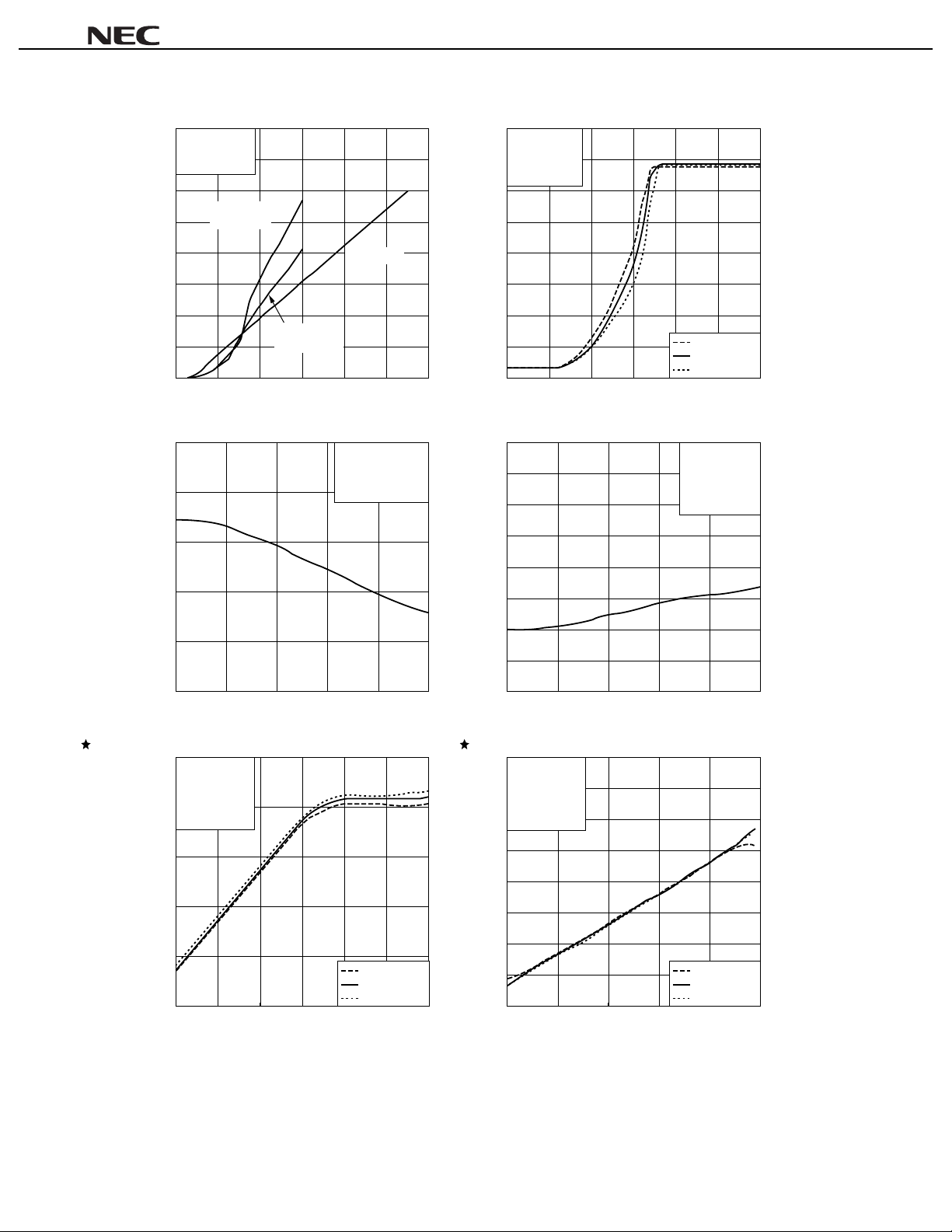
TYPICAL CHARACTERISTICS (TA = 25
CIRCUIT CURRENT vs. SUPPLY VOLTAGE
40
No input signal
measurement
35
circuit1, 3
30
(mA)
25
CC
20
15
Circuit Current I
10
25
20
15
10
AGC
AGC
= 0 V)
(V
5
0
024
Supply Voltage V
GAIN vs. INPUT FREQUENCY
Video Amp.
AGC
AGC
= VCC1)
(V
6 8 10 12
CC
(V)
VCC1 = V
P
in
= -60 dBm
measurement
circuit2
C)
°°°°
AGC
Note1
= 5 V
50
fin = 100 MHz
L
= 560 Ω
R
40
measurement
circuit2
30
20
10
Gain (dB)
0
-
10
-
20
-
30
012
-
20
-
30
-
40
GAIN vs. INPUT FREQUENCY
GAIN vs. AGC VOLTAGE
3456
AGC
AGC Voltage V
(V)
VCC1 = 5 V
V
P
measurement
circuit2
CC
1 = 4.5 V
V
V
CC
1 = 5.0 V
CC
1 = 5.5 V
V
AGC
= 0 V
in
= -15 dBm
Note1
Gain (50 Ω/560 Ω) (dB)
5
0
0 100 200
OUTPUT POWER vs. INPUT POWER
0
V
AGC
= VCC1
in
= 100 MHz
f
L
= 560 Ω
R
-
10
measurement
Note2
circuit2
-
20
(50 Ω/560 Ω) (dBm)
out
-
30
-
40
Output Power P
-
50
-
60-50-40
Input Frequency f
Input Power P
300 400 500
in
(MHz)
VCC1 = 4.5 V
V
CC
1 = 5.0 V
CC
1 = 5.5 V
V
-
30-20-10 0
in
(dBm)
Notes 1.2.Gain = (Gain at Spectrum Analyzer) + 20 log (560 Ω/50 Ω)
Output Power = (Output Power at Spectrum Analyzer) + 10 log (560 Ω/50 Ω)
Gain (50 Ω/560 Ω) (dB)
-
50
-
60
0 100 200
-
10
-
20
-
30
-
40
-
50
(50 Ω/560 Ω) (dBm)
out
-
60
-
70
Output Power P
-
80
-
90
OUTPUT POWER vs. INPUT POWER
V
AGC
= 0 V
in
= 100 MHz
f
L
= 560 Ω
R
measurement
Note2
circuit2
-
35
-
Input Frequency f
25
-
15
Input Power P
300 400 500
in
(MHz)
VCC1 = 4.5 V
V
CC
1 = 5.0 V
CC
1 = 5.5 V
V
-
5155
in
(dBm)
8
Data Sheet P13710EJ3V0DS00
Page 9
µµµµ
PC3206GR
TYPICAL CHARACTERISTICS (TA = 25
DIFFERENTIAL GAIN vs. INPUT FREQUENCY
450
400
350
(V/V)
300
video
250
200
150
Differential Gain G
100
V
CC
50
0
CC
V
CC
V
2 = 8 V
2 = 9 V
2 = 10 V
0 50 100
Input Frequency f
DIFFERENTIAL GAIN vs. INPUT FREQUENCY
250
200
(V/V)
video
150
fin = 100 MHz
L
= 1 kΩ
R
G1A-G1B
= SHORT
measurement
circuit4
150 200 250
in
(MHz)
fin = 100 MHz
L
= 1 kΩ
R
G1A-G1B
= SHORT
measurement
circuit4
C)
°°°°
DIFFERENTIAL GAIN vs. INPUT FREQUENCY
40
35
fin = 100 MHz
L
= 1 kΩ
R
G1A-G1B
= OPEN
30
(V/V)
25
video
measurement
circuit4
20
15
10
Differential Gain G
V
CC
5
0
0 50 100
40
35
2 = 8 V
CC
2 = 9 V
V
CC
2 = 10 V
V
150 200 250
Input Frequency f
in
(MHz)
DIFFERENTIAL GAIN vs. INPUT FREQUENCY
fin = 100 MHz
L
= 1 kΩ
R
G1A-G1B
= OPEN
30
(V/V)
25
video
measurement
circuit4
20
100
Differential Gain G
50
V
CC
2 = 4.5 V
CC
2 = 5.0 V
V
CC
2 = 5.5 V
V
0
0 50 100
OUTPUT POWER vs. INPUT POWER
0
-
5
-
10
) (dBm)
Ω
/1 k
-
15
Ω
(50
-
20
out
-
25
-
30
Output Power P
-
35
-
40
-
50
VCC2 = 9 V
-
40
Input Frequency f
V
CC
2 = 5 V
-
30
Input Power P
150 200 250
in
(MHz)
fin = 100 MHz
L
= 1 kΩ
R
G1A-G1B
= SHORT
measurement
Note
circuit4
-
20
in
(dBm)
-
10 0
15
10
Differential Gain G
5
0
0 50 100
0
-
10
) (dBm)
Ω
-
20
/1 k
Ω
(50
-
30
out
-
40
-
50
Output Power P
-
60
-
50
Note Output Power = (Output Power at Spectrum Analyzer) + 10 log (1 kΩ/50 Ω)
CC
2 = 4.5 V
V
CC
2 = 5.0 V
V
CC
2 = 5.5 V
V
150 200 250
Input Frequency f
in
(MHz)
OUTPUT POWER vs. INPUT POWER
VCC2 = 5 V
VCC2 = 9 V
fin = 100 MHz
R
L
= 1 kΩ
G1A-G1B
= OPEN
measurement
circuit4
-
40
-
30
-
20
-
10 0 10
Input Power P
in
(dBm)
Note
Data Sheet P13710EJ3V0DS00
9
Page 10
µµµµ
PC3206GR
STANDARD CHARACTERISTICS (TA = 25
OUTPUT POWER vs. INPUT POWER
0
-
10
V
AGC
-
20
V
AGC
) (dBm)
Ω
-
30
/560
Ω
-
40
(50
out
-
50
-
60
-
70
Output Power P
-
80
-
90
= 5 V
V
AGC
= 2.8 V
V
AGC
= 2 V
-
60
-
40
Input Power P
-
20 0 20
in
(dBm)
3rd ORDER INTERMODULATION DISTORTION
0
= 3.25 V
V
AGC
VCC1 = 5 V
f
in
= 100 MHz
R
L
= 560 Ω
measurement
circuit2
C)
°°°°
= 0 V
Note
NOISE FIGURE vs. INPUT FREQUENCY
10
V
AGC
= VCC1
R
L
= 560 Ω
9
measurement
circuit5
8
7
6
5
4
3
Noise Figure NF (dB)
2
1
0
10 100
Input Frequency f
in
(MHz)
VCC1 = 4.5 V
V
CC
1 = 5.0 V
V
CC
1 = 5.5 V
1000
-
20
) (dBm)
Ω
/560
-
40
Ω
(50
out
-
60
-
80
Output Power P
-
100
-
50
-
45
-
40
-
35
Input Power P
VCC1 = V
f
f
R
measurement
circuit2
-
in
(dBm)
AGC
in
1 = 100 MHz
in
2 = 106 MHz
L
= 560 Ω
Note
30
-
25 –20
= 5 V
Note Output Power = (Output Power at Spectrum Analyzer) + 10 log (560 Ω/50 Ω)
10
Data Sheet P13710EJ3V0DS00
Page 11

µµµµ
PC3206GR
STANDARD CHARACTERISTICS (TA = 25
3rd ORDER INTERMODULATION DISTORTION
0
-
10
-
20
) (dBm)
Ω
-
30
/1 k
Ω
-
40
-
50
-
60
-
70
Output Power Pout (50
-
80
-
90
-
50
3rd ORDER INTERMODULATION DISTORTION
0
-
40
Input Power P
-
30
in (dBm)
VCC2 = 9 V
fin = 100 MHz
fin2 = 106 MHz
RL = 1 kΩ
G1A-G1B
= SHORT
measurement
circuit4
-
20
Note
C)
°°°°
3rd ORDER INTERMODULATION DISTORTION
0
-
10
-
20
) (dBm)
Ω
-
30
/1 k
Ω
-
40
-
50
-
60
-
70
Output Power Pout (50
-
80
-
-
10
90
-
50
3rd ORDER INTERMODULATION DISTORTION
0
-
40
Input Power P
-
30
in (dBm)
VCC2 = 5 V
fin = 100 MHz
fin2 = 106 MHz
RL = 1 kΩ
G1A-G1B
= SHORT
measurement
Note
circuit4
-
20
-
10
-
10
-
20
) (dBm)
Ω
-
30
/1 k
Ω
-
40
-
50
-
60
-
70
Output Power Pout (50
-
80
-
90
-
25
Note Output Power = (Output Power at Spectrum Analyzer) + 10 log (1 kΩ/50 Ω)
-
20
Input Power P
-
15
-
10
in (dBm)
VCC2 = 9 V
fin = 100 MHz
fin2 = 106 MHz
RL = 1 kΩ
G1A-G1B
= OPEN
measurement
Note
circuit4
-
50
-
10
-
20
) (dBm)
Ω
-
30
/1 k
Ω
-
40
-
50
-
60
-
70
Output Power Pout (50
-
80
-
90
-
25
-
20
Input Power P
VCC2 = 5 V
fin = 100 MHz
fin2 = 106 MHz
RL = 1 kΩ
G1A-G1B
= OPEN
measurement
Note
circuit4
-
15
-
10
in (dBm)
-
50
Data Sheet P13710EJ3V0DS00
11
Page 12

µµµµ
PC3206GR
STANDARD CHARACTERISTICS (TA = 25
100
80
60
VCC1 = 5 V
Gain (dB)
VCC2 = 9 V
40
VAGC = 5 V
fin1 = 100 MHz
RL = 1 kΩ
20
G1A-G1B
= SHORT
measurement
circuit6
0
0 100
70
60
50
40
VCC1 = 5 V
30
Gain (dB)
VCC2 = 9 V
VAGC = 3 V
fin1 = 100 MHz
20
RL = 1 kΩ
G1A-G1B
10
= SHORT
measurement
circuit6
0
0 100
25
20
15
VCC1 = 5 V
V
Gain (dB)
10
V
f
in
R
5
G1A-G1B
= SHORT
measurement
circuit6
0
0 100
GAIN vs. INPUT FREQUENCY
200 300 400 500
Input Frequency f
GAIN vs. INPUT FREQUENCY
200 300 400 500
Input Frequency f
GAIN vs. INPUT FREQUENCY
CC
2 = 9 V
AGC
= 0 V
1 = 100 MHz
L
= 1 kΩ
200 300 400 500
Input Frequency f
in (MHz)
in (MHz)
in (MHz)
C)
°°°°
GAIN vs. INPUT FREQUENCY
100
80
60
VCC1 = 5 V
Gain (dB)
VCC2 = 5 V
40
VAGC = 5 V
fin1 = 100 MHz
RL = 1 kΩ
20
G1A-G1B
= SHORT
measurement
circuit6
0
0 100
200 300 400 500
Input Frequency f
in (MHz)
GAIN vs. INPUT FREQUENCY
70
VCC1 = 5 V
VCC2 = 5 V
60
VAGC = 3 V
fin1 = 100 MHz
50
RL = 1 kΩ
G1A-G1B
= SHORT
40
30
Gain (dB)
measurement
circuit6
20
10
0
0 100
200 300 400 500
Input Frequency f
in (MHz)
GAIN vs. INPUT FREQUENCY
25
20
VCC1 = 5 V
V
CC
2 = 5 V
V
AGC
= 0 V
f
in
1 = 100 MHz
R
L
= 1 kΩ
G1A-G1B
15
= SHORT
measurement
circuit6
Gain (dB)
10
5
0
0 100
200 300 400 500
Input Frequency f
in (MHz)
12
Data Sheet P13710EJ3V0DS00
Page 13

µµµµ
PC3206GR
STANDARD CHARACTERISTICS (TA = 25
80
60
40
VCC1 = 5 V
Gain (dB)
VCC2 = 9 V
VAGC = 5 V
f
RL = 1 kΩ
20
G1A-G1B
= OPEN
measurement
circuit6
0
0 100
40
30
20
VCC1 = 5 V
Gain (dB)
VCC2 = 9 V
VAGC = 3 V
fin1 = 100 MHz
RL = 1 kΩ
10
G1A-G1B
= OPEN
measurement
circuit6
0
0 100
GAIN vs. INPUT FREQUENCY
in1 = 100 MHz
200 300 400 500
Input Frequency f
GAIN vs. INPUT FREQUENCY
200 300 400 500
Input Frequency f
in (MHz)
in (MHz)
C)
°°°°
80
60
40
VCC1 = 5 V
Gain (dB)
VCC2 = 5 V
VAGC = 5 V
f
RL = 1 kΩ
20
G1A-G1B
= OPEN
measurement
circuit6
0
0 100
40
30
20
Gain (dB)
10
0
0 100
GAIN vs. INPUT FREQUENCY
in1 = 100 MHz
200 300 400 500
Input Frequency f
GAIN vs. INPUT FREQUENCY
200 300 400 500
Input Frequency f
in (MHz)
VCC1 = 5 V
VCC2 = 5 V
VAGC = 3 V
fin1 = 100 MHz
RL = 1 kΩ
G1A-G1B
= OPEN
measurement
circuit6
in (MHz)
Data Sheet P13710EJ3V0DS00
13
Page 14

µµµµ
PC3206GR
STANDARD CHARACTERISTICS (TA = 25
3rd ORDER INTERMODULATION DISTORTION
0
-
10
-
20
(50 Ω/1 kΩ) (dBm)
-
30
out
-
40
-
50
Output Power P
-
60
-
70
-
65
-
60
Input Power P
3rd ORDER INTERMODULATION DISTORTION
0
-
20
VCC1 = 5 V
VCC2 = 9 V
V
f
fin2 = 106 MHz
RL = 1 kΩ
G1A-G1B
= SHORT
measurement
circuit6
in
(dBm)
AGC
= 5 V
in
1 = 100 MHz
-
55
Note
C)
°°°°
3rd ORDER INTERMODULATION DISTORTION
0
-
10
-
20
(50 Ω/1 kΩ) (dBm)
-
30
out
-
40
-
50
Output Power P
-
60
-
-
50
70
-
65
-
60
Input Power P
in
(dBm)
VCC1 = 5 V
VCC2 = 5 V
V
AGC
= 5 V
fin1 = 100 MHz
fin2 = 106 MHz
RL = 1 kΩ
G1A-G1B
= SHORT
measurement
Note
circuit6
-
55
-
50
(50 Ω/1 kΩ) (dBm)
-
40
out
-
60
Output Power P
-
80
-
15
-
10
-
50 5
Input Power P
3rd ORDER INTERMODULATION DISTORTION
0
-
20
(50 Ω/1 kΩ) (dBm)
-
40
out
-
60
Output Power P
-
80
-
60
-
50
Input Power P
VCC1 = 5 V
VCC2 = 9 V
V
f
fin2 = 106 MHz
RL = 1 kΩ
G1A-G1B
= SHORT
measurement
circuit6
in
(dBm)
VCC1 = 5 V
VCC2 = 9 V
V
f
fin2 = 106 MHz
RL = 1 kΩ
G1A-G1B
= OPEN
measurement
circuit6
-
40
in
(dBm)
AGC
= 0 V
in
1 = 100 MHz
Note
AGC
= 5 V
in
1 = 100 MHz
Note
3rd ORDER INTERMODULATION DISTORTION
0
-
20
(50 Ω/1 kΩ) (dBm)
-
40
out
-
60
Output Power P
-
-
30
80
-
60
Note Output Power = (Output Power at Spectrum Analyzer) + 10 log (1 kΩ/50 Ω)
-
50
Input Power P
-
in
(dBm)
40
VCC1 = 5 V
VCC2 = 5 V
V
AGC
= 5 V
f
in
1 = 100 MHz
fin2 = 106 MHz
RL = 1 kΩ
G1A-G1B
= OPEN
measurement
Note
circuit6
-
30
14
Data Sheet P13710EJ3V0DS00
Page 15

µµµµ
PC3206GR
STANDARD CHARACTERISTICS (TA = 25
NOISE FIGURE vs. INPUT FREQUENCY
10
9
8
7
6
5
VCC1 = 5 V
4
VCC2 = 9 V
VAGC = 5 V
3
Noise Figure NF (dB)
RL = 1 kΩ
2
G1A-G1B
= SHORT
1
measurement
circuit7
0
10 100
Input Frequency f
NOISE FIGURE vs. INPUT FREQUENCY
10
in (MHz)
C)
°°°°
NOISE FIGURE vs. INPUT FREQUENCY
10
9
8
7
6
5
VCC1 = 5 V
4
VCC2 = 5 V
VAGC = 5 V
3
Noise Figure NF (dB)
RL = 1 kΩ
2
G1A-G1B
= SHORT
1
measurement
circuit7
0
1000
10 100
Input Frequency f
NOISE FIGURE vs. INPUT FREQUENCY
10
1000
in (MHz)
9
8
7
6
5
VCC1 = 5 V
4
VCC2 = 9 V
VAGC = 5 V
3
Noise Figure NF (dB)
RL = 1 kΩ
2
G1A-G1B
= OPEN
1
measurement
circuit7
0
10 100
Input Frequency f
in (MHz)
1000
9
8
7
6
5
VCC1 = 5 V
4
VCC2 = 5 V
VAGC = 5 V
3
Noise Figure NF (dB)
RL = 1 kΩ
2
G1A-G1B
= OPEN
1
measurement
circuit7
0
10 100
Input Frequency f
1000
in (MHz)
Data Sheet P13710EJ3V0DS00
15
Page 16

INPUT IMPEDANCE (2 PIN)
µµµµ
PC3206GR
START 0.045000000 GHz
STOP 0.250000000 GHz
OUTPUT IMPEDANCE (20 PIN)
MARKER Z
1 45 MHz 938.4 Ω – j604.8
2 100 MHz 434.7 Ω – j573.8
3 250 MHz 122.5 Ω – j324.9
Conditions TA = 25°C
CC
V
1
2
3
1 = 5 V
in
Ω
Ω
Ω
2
3
1
START 0.045000000 GHz
STOP 0.250000000 GHz
MARKER Z
1 45 MHz 19.86 Ω + 3.83
2 100 MHz 20.28 Ω + 9.26
3 250 MHz 22.28 Ω + 22.48
Conditions TA = 25°C
CC
V
1 = 5 V
out
Ω
Ω
Ω
16
Data Sheet P13710EJ3V0DS00
Page 17

INPUT IMPEDANCE (19 PIN)
µµµµ
PC3206GR
START 0.045000000 GHz
STOP 0.250000000 GHz
OUTPUT IMPEDANCE (17 PIN)
MARKER Z
1 45 MHz 965.8 Ω – j601.2
2 100 MHz 446.6 Ω – j661.8
3 250 MHz 126.8 Ω – j312.4
Conditions TA = 25°C
CC
V
1
2
3
1 = 5 V
in
Ω
Ω
Ω
2
3
1
START 0.045000000 GHz
STOP 0.250000000 GHz
MARKER Z
1 45 MHz 10.32 Ω + j2.88
2 100 MHz 10.86 Ω + j6.42
3 250 MHz 12.67 Ω + j15.39
Conditions TA = 25°C
CC
V
1 = 5 V
OUT
Ω
Ω
Ω
Data Sheet P13710EJ3V0DS00
17
Page 18

INPUT IMPEDANCE (15 PIN)
(i) TA = 25°C, VCC2 = 5 V
µµµµ
PC3206GR
START 0.045000000 GHz
STOP 0.250000000 GHz
MARKER Z
1 45 MHz 840.0 Ω – j2560
2 100 MHz 50.19 Ω – j1259
3 250 MHz 52.03 Ω – j475.6
1
2
3
in
Ω
Ω
Ω
(ii) TA = 25°C, VCC2 = 9 V
START 0.045000000 GHz
STOP 0.250000000 GHz
MARKER Z
1 45 MHz 478.3 Ω – j3091
2 100 MHz 106.13 Ω – j1368
3 250 MHz 55.11 Ω – j501.3
1
2
3
in
Ω
Ω
Ω
18
Data Sheet P13710EJ3V0DS00
Page 19

OUTPUT IMPEDANCE (12 PIN)
µµµµ
PC3206GR
(i) TA = 25°C, VCC2 = 5 V, 11 pin is grounded through 50
2
3
1
START 0.045000000 GHz
STOP 0.250000000 GHz
resistor.
ΩΩΩΩ
MARKER Z
1 45 MHz 9.88 Ω + j6.25
2 100 MHz 14.21 Ω + j11.78
3 250 MHz 23.64 Ω + j15.73
out
Ω
Ω
Ω
(ii) TA = 25°C, VCC2 = 9 V, 11 pin is grounded through 50
2
3
1
START 0.045000000 GHz
STOP 0.250000000 GHz
resistor.
ΩΩΩΩ
MARKER Z
1 45 MHz 7.36 Ω + j4.85
2 100 MHz 10.50 Ω + j9.58
3 250 MHz 19.37 Ω + j13.70
out
Ω
Ω
Ω
Data Sheet P13710EJ3V0DS00
19
Page 20

THERMAL CHARACTERISTICS (FOR REFERENCE)
µµµµ
PC3206GR
CIRCUIT CURRENT vs. AMBIENT TEMPERATURE
(AGC BLOCK)
30
no input signal
CC
1 = 5 V
V
measurement
25
circuit1
V
20
(mA)
CC
15
AGC
AGC
V
10
Circuit Current I
5
0
-
50
-
25 0 25 50 75
A
Ambient Temperature T
(°C)
OUTPUT POWER vs. INPUT POWER
0
VCC1 = 5 V
AGC
= VCC1
V
in
= 100 MHz
f
L
= 560 Ω
R
-
10
measurement
Note
circuit2
-
20
= 0 V
= 5 V
100
CIRCUIT CURRENT vs. AMBIENT TEMPERATURE
(VIDEO AMP BLOCK)
30
no input signal
measurement
circuit3
25
VCC2 = 9 V
20
(mA)
CC
15
CC
10
V
Circuit Current I
5
0
-
50
-
25 0 25 50 75
A
Ambient Temperature T
(°C)
OUTPUT POWER vs. INPUT POWER
-
10
VCC1 = 5 V
AGC
= 0 V
V
-
20
in
= 100 MHz
f
L
= 560 Ω
R
-
30
measurement
Note
circuit2
-
40
2 = 5 V
100
-
(50 Ω/560 Ω) (dBm)
out
-
30
-
40
Output Power P
-
50
-
60
-
50
-
40
-
30
Input Power P
in
(dBm)
-
20
TA = -40 °C
A
= +25 °C
T
A
= +85 °C
T
-
10
0
50
(50 Ω/560 Ω) (dBm)
out
-
60
-
70
Output Power P
-
80
-
90
-
35
Note Output Power = (Output Power at Spectrum Analyzer) + 10 log (560 Ω/50 Ω)
-
25
Input Power P
TA = -40 °C
A
= +25 °C
T
A
= +85 °C
T
-
15
-
55
in
(dBm)
15
20
Data Sheet P13710EJ3V0DS00
Page 21

THERMAL CHARACTERISTICS (FOR REFERENCE)
µµµµ
PC3206GR
DIFFERENTIAL GAIN vs. INPUT FREQUENCY
450
400
350
300
250
200
150
Differential Gain Gvideo (V/V)
100
TA = -40 °C
50
TA = +25 °C
TA = +85 °C
0
0 50 100 150 200
in (MHz)
50
VCC1 = 5 V
fin = 100 MHz
40
RL = 560 Ω
measurement
30
circuit2
Input Frequency f
GAIN vs. AGC VOLTAGE
VCC2 = 9 V
fin = 100 MHz
RL = 1 kΩ
G1A-G1B
= SHORT
measurement
circuit4
250
DIFFERENTIAL GAIN vs. INPUT FREQUENCY
250
200
150
100
Differential Gain Gvideo (V/V)
50
TA = -40 °C
TA = +25 °C
TA = +85 °C
0
0 50 100 150 200
Input Frequency f
in (MHz)
VCC2 = 5 V
fin = 100 MHz
RL = 1 kΩ
G1A-G1B
= SHORT
measurement
circuit4
250
20
10
Gain (dB)
0
-
10
-
20
-
30
012345
AGC Voltage V
AGC (V)
TA = -40 °C
TA = +25 °C
TA = +85 °C
6
Data Sheet P13710EJ3V0DS00
21
Page 22

MEASUREMENT CIRCUIT 1
0.022 F
µ
V
AGC
1 F
µ
VCC1
100 k
1 F 0.022 F
µ
0.022 F
0.1 F
µ
0.1 F
100 k
µ
µµµµ
PC3206GR
200
1 AGC Amp1
2IN
20
4700pF
19
µ
318
417
µ
516
615
AGC Amp2
1 F
µµ
510
0.1 F
0.1 F
µ
VCC1
AGC OUT
0.022 F
0.1 F
µ
MEASUREMENT CIRCUIT 2
Note
SG1
(50 Ω)
V
AGC
MIXPAD
VCC1
SG2
(50 Ω)
100 k
1 F
µ
1 F 0.022 F
µ
0.022 F
0.1 F
0.022 F
100 k
µ
µ
µ
0.1 F
714
µ
813
912
10 11
1 AGC Amp1
2
VIDEO
Amp
200
20
4700pF
19
µ
318
417
µ
516
615
AGC Amp2
1 F
µµ
510
0.1 F
0.1 F
µ
Spectrum
Analyzer
(50 Ω)
VCC1
22
0.1 F
In the case of measurement of IM
Note
0.022 F
µ
µ
714
813
912
10 11
3
VIDEO
Amp
Data Sheet P13710EJ3V0DS00
Page 23

MEASUREMENT CIRCUIT 3
µµµµ
PC3206GR
1 AGC Amp1
219
318
417
516
615
714
open
/short
813
912
10 11
MEASUREMENT CIRCUIT 4
VIDEO
Amp
AGC Amp2
20
0.1 F
1000pF
0.022 F
µ
0.022 F 950
µ
0.022 F 950
µ
µ
IN1
51
VCC2
OUT1
OUT2
1 AGC Amp1
219
318
417
516
615
714
open
/short
In the case of measurement of IM
Note
813
912
10 11
VIDEO
Amp
20
Note
AGC Amp2
0.1 F
1000pF
0.022 F
0.022 F 950
µ
0.022 F
µ
3
SG1
(50 Ω)
µ
MIXPAD
51
µ
1 k
SG2
(50 Ω)
VCC2
Spectrum
Analyzer
(50 Ω)
Data Sheet P13710EJ3V0DS00
23
Page 24

MEASUREMENT CIRCUIT 5
µµµµ
PC3206GR
VIDEO
Amp
NF
METER
AGC Amp2
200
20
4700pF
19
1 F
µµ
510
0.1 F
0.1 F
µ
VCC1
Noise Source
1 AGC Amp1
0.022 F
µ
2
AGC
V
1 F
µ
VCC1
100 k
µ
1 F 0.022 F
0.022 F
0.1 F
µ
100 k
µ
0.1 F
µ
0.022 F
0.1 F
µ
318
417
µ
516
615
714
µ
813
912
10 11
MEASUREMENT CIRCUIT 6
SG1
(50 Ω)
V
AGC
1 F
µ
VCC1
0.022 F
µ
100 k
1 F 0.022 F
µ
0.022 F
0.1 F
µ
0.022 F
0.1 F
µ
100 k
µ
µ
open
/short
0.1 F
µ
200
1 AGC Amp1
2
318
417
µ
516
615
714
813
912
10 11
VIDEO
Amp
AGC Amp2
20
4700pF
19
1 F
µµ
510
1000pF
0.022 F 950
0.022 F
0.1 F
0.022 F
µ
µ
µ
1 k
0.1 F
µ
Spectrum
Analyzer
(50 Ω)
VCC1
VCC2
24
Data Sheet P13710EJ3V0DS00
Page 25

MEASUREMENT CIRCUIT 7
µµµµ
PC3206GR
VIDEO
Amp
NF
METER
AGC Amp2
200
20
4700pF
19
1 F
µµ
510
1000pF
0.022 F 950
0.022 F
0.1 F
0.022 F
µ
µ
µ
1 k
0.1 F
µ
VCC1
VCC2
NOISE
SOURCE
1 AGC Amp1
0.022 F
µ
2
V
AGC
1 F
µ
VCC1
100 k
1 F 0.022 F
µ
0.022 F
0.1 F
µ
0.022 F
0.1 F
µ
100 k
µ
µ
open
/short
0.1 F
µ
318
417
µ
516
615
714
813
912
10 11
Data Sheet P13710EJ3V0DS00
25
Page 26

ILLUSTRATION OF THE EVALUATION BOARD FOR MEASUREMENT CIRCUIT6
AGC IN AGC OUT VDEO IN
VCC
VAGC
µ
VCC
µ
1F
0.022
1F
100 k
0.022
µ
0.1
200
4700 P
0.1
510
µ
1
µ
µ
0.1
100 k
µ
0.1
µ
µ
0.022
µ
µµµµ
PC3206GR
0.022
µ
PC3206
Notes on evaluation board
(1) GND pattern on rear side
(2) : Through hole
(3) : represents cutout
µ
µ
0.1
short/open
NEC
FXTR
µ
0.022
950 950
0.022
0.022
µ
1000 P
µ
VCC
VDEO OUTVDEO OUT
26
Data Sheet P13710EJ3V0DS00
Page 27

PACKAGE DIMENSIONS
20 PIN PLASTIC SSOP (225 mil) (UNIT: mm)
µµµµ
PC3206GR
20
110
6.7 ± 0.3
1.8 MAX.
1.5 ± 0.1
11
detail of lead end
3˚
6.4 ± 0.2
4.4 ± 0.1
+7˚
–3˚
1.0 ± 0.2
NOTE
0.5 ± 0.2
0.15
+0.10
–0.05
0.1 ± 0.1
0.65
0.22
+0.10
–0.05
0.10
0.15
M
0.575 MAX.
Each lead centerline is located within 0.10 mm of its true position (T.P.) at maximum material condition.
Data Sheet P13710EJ3V0DS00
27
Page 28

µµµµ
PC3206GR
NOTE ON CORRECT USE
(1) Observe precautions for handling because of electro-static sensitive devices.
(2) Form a ground pattern as wide as possible to minimize ground impedance (to prevent undesires osillation).
(3) Keep the track length of the ground pins as short as possible.
CC
(4) A low pass filter must be attached to V
line.
(5) A matching circuit must be externally attached to output port.
RECOMMENDED SOLDERING CONDITIONS
This product should be soldered under the following recommended conditions. For soldering methods and
conditions other than those recommended below, contact your NEC sales representative.
Soldering Method Soldering Conditions
Infrared Reflow Package peak t em perature: 235°C or below
Time: 30 seconds or less (at 210°C)
Count: 3, Exposure limi t
VPS P ackage peak temperature: 215°C or below
Time: 40 seconds or less (at 200°C)
Count: 3, Exposure limi t
Partial Heating Pin temperature: 300° C
Time: 3 seconds or less (per side of device)
Exposure limit
After opening the dry pack, keep it in a place below 25°C and 65% RH for the allowable storage period.
Note
Note
: None
Note
Note
: None
: None
Recommended Condition
Symbol
IR35-00-3
VP15-00-3
–
Caution Do not use different soldering methods together (except for partial heating).
For details of the recommended soldering conditions for surface mounting, refer to infor mation document
SEMICONDUCTOR DEVICE MOUNTING TECHNOLOGY MANUAL (C10535E)
.
28
Data Sheet P13710EJ3V0DS00
Page 29

[MEMO]
µµµµ
PC3206GR
Data Sheet P13710EJ3V0DS00
29
Page 30

[MEMO]
µµµµ
PC3206GR
30
Data Sheet P13710EJ3V0DS00
Page 31

[MEMO]
µµµµ
PC3206GR
Data Sheet P13710EJ3V0DS00
31
Page 32

µµµµ
PC3206GR
• The information in this document is subject to change without notice. Before using this document, please
confirm that this is the latest version.
• No part of this document may be copied or reproduced in any form or by any means without the prior written
consent of NEC Corporation. NEC Corporation assumes no responsibility for any errors which may appear in
this document.
• NEC Corporation does not assume any liability for infringement of patents, copyrights or other intellectual property
rights of third parties by or arising from use of a device described herein or any other liability arising from use
of such device. No license, either express, implied or otherwise, is granted under any patents, copyrights or other
intellectual property rights of NEC Corporation or others.
• Descriptions of circuits, software, and other related information in this document are provided for illustrative
purposes in semiconductor product operation and application examples. The incorporation of these circuits,
software, and information in the design of the customer's equipment shall be done under the full responsibility
of the customer. NEC Corporation assumes no responsibility for any losses incurred by the customer or third
parties arising from the use of these circuits, software, and information.
• While NEC Corporation has been making continuous effort to enhance the reliability of its semiconductor devices,
the possibility of defects cannot be eliminated entirely. To minimize risks of damage or injury to persons or
property arising from a defect in an NEC semiconductor device, customers must incorporate sufficient safety
measures in its design, such as redundancy, fire-containment, and anti-failure features.
• NEC devices are classified into the following three quality grades:
"Standard", "Special", and "Specific". The Specific quality grade applies only to devices developed based on a
customer designated "quality assurance program" for a specific application. The recommended applications of
a device depend on its quality grade, as indicated below. Customers must check the quality grade of each device
before using it in a particular application.
Standard: Computers, office equipment, communications equipment, test and measurement equipment,
audio and visual equipment, home electronic appliances, machine tools, personal electronic
equipment and industrial robots
Special: Transportation equipment (automobiles, trains, ships, etc.), traffic control systems, anti-disaster
systems, anti-crime systems, safety equipment and medical equipment (not specifically designed
for life support)
Specific: Aircraft, aerospace equipment, submersible repeaters, nuclear reactor control systems, life
support systems or medical equipment for life support, etc.
The quality grade of NEC devices is "Standard" unless otherwise specified in NEC's Data Sheets or Data Books.
If customers intend to use NEC devices for applications other than those specified for Standard quality grade,
they should contact an NEC sales representative in advance.
M7 98. 8
 Loading...