

Page 1
DATA SHEET
BIPOLAR ANALOG INTEGRATED CI RCUIT
µµµµ
PC3205GR
IQ DEMODULATOR FOR DIGITAL VIDEO/DATA RECEIVER
DESCRIPTION
The µPC3205GR is Silicon monolithic IC designed for use as IQ demodulator in digital communication systems.
This IC consists of AGC amplifier, dual balanced mixers (DBM), oscillator, quadrature phase shifter and I & Q output
buffer amplifiers.
The package is 20-pin SSOP (shrink small outline package) suitable for high-density surface mount.
FEATURES
• On chip quadrature (90°) phase shifter
• IQ phase and amplitude balance Amplitude Balance :
Phase Balance :
• Low distortion IM
• Supply Voltage V
• Packaged in 20-pin SSOP suitable for high-density surface mount
3
CC
0.5 dB
±
2.0 degree
±
: 56 dBc (@0.708 V
:5 V
P-P
/tone)
ORDERING INFORMATION
Part Number Package Supplying Form
µ
PC3205GR-E1 20-pin plastic SSOP (225 mil) Embossed tape 12 mm wide.
Pin 1 indicates pull-out di rection of tape.
Q’ty 2.5 k/reel
For evaluation sample order, please contact your local NEC office. (Part number for sample order: µPC3205GR)
Caution electro-static sensitive device
The information in this document is subject to change without notice. Before using this document, please
confirm that this is the latest version.
Not all devices/types available in every country. Please check with local NEC representative for
availability and additional information.
Document No. P13541EJ3V0DS00 (3rd edition)
Date Published October 1999 N CP(K)
Printed in Japan
The mark shows major revised points.
©
1998, 1999
Page 2
INTERNAL BLOCK DIAGRAM AND PIN CONFIGURATION (Top View)
µµµµ
PC3205GR
V
CC
(I)
GND (I)
AGC
V
GND (IF)
IF IN
IF IN
GND (IF)
CC
(IF)
V
GND (Q)
V
CC
(Q)
1
2
3
4
5
6
7
8
9
10
IF
Amplifier
AGC
Amplifier
MIXER
90 deg
phase
shifter
0°
90°
LPF
LPF
OSC
20
19
18
17
16
15
14
13
12
11
I OUT
GND (PS)
V
CC
(PS)
OSC-C1
OSC-B2
OSC-B1
OSC-C2
GND (PS)
GND (PS)
Q OUT
2
Data Sheet P13541EJ3V0DS00
Page 3
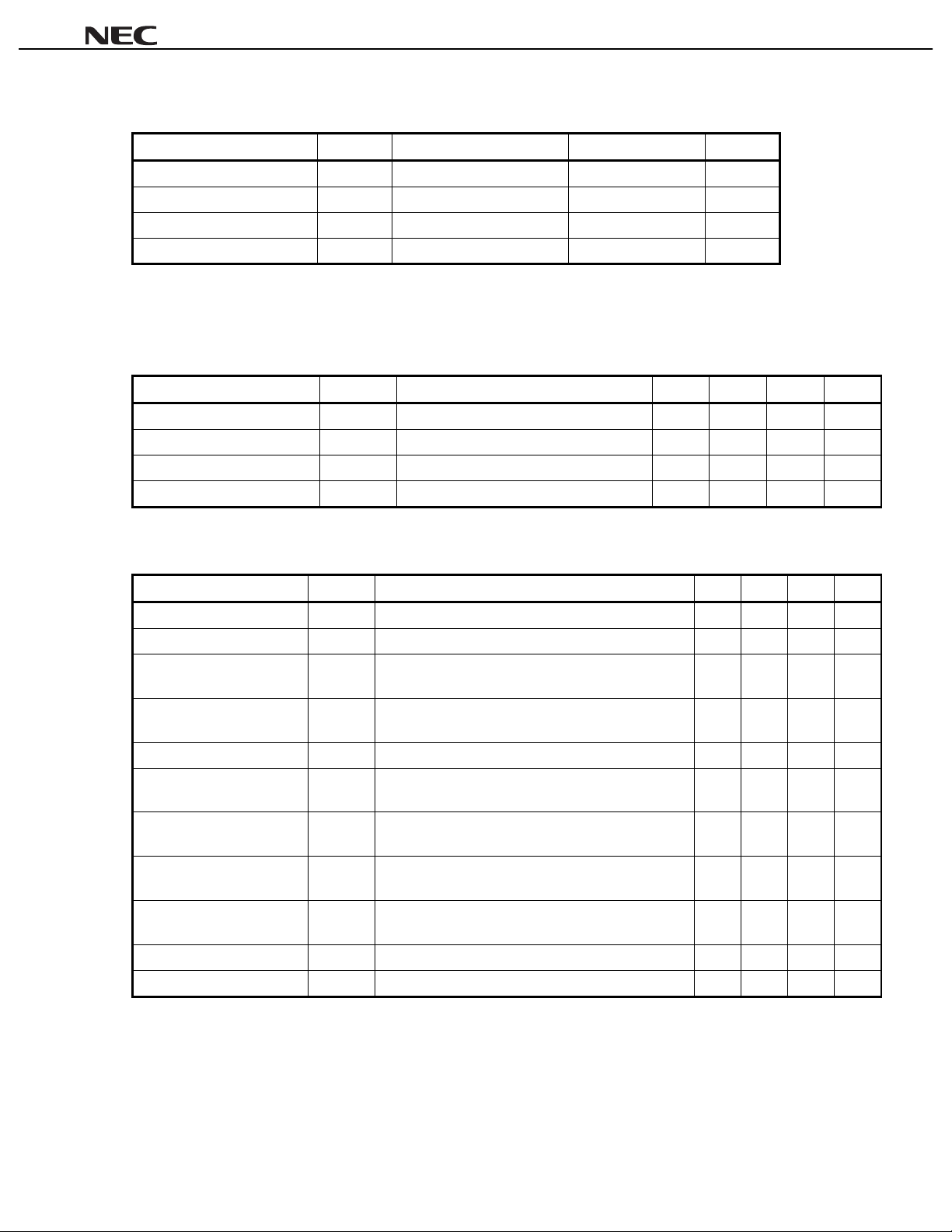
PIN FUNCTIONS
µµµµ
PC3205GR
Pin
No.
Pin
Name
1VCC(I) 5.0 Supply voltage pin.
2 GND(I) 0.0 Ground pin.
3V
4 GND(IF) 0.0 Ground pin.
5IF IN 2.7
AGC
Pin Voltage
TYP. (V)
0 to 5 Gain control pin.
AGC
V
= 0 V: Full gain
AGC
V
= 5 V: Full reduction
IF input pins. In case of single input, 5 pin or
6 pin should be grounded through capacitor.
Function and Explanation Equivalent Circuit
3
6IF IN 2.7
7 GND(IF) 0.0 Ground pin.
8VCC(IF) 5.0 Supply voltage pin.
9 GND (Q) 0.0 Ground pin.
10 VCC (Q) 5.0 Supply voltage pin.
5
6
Data Sheet P13541EJ3V0DS00
3
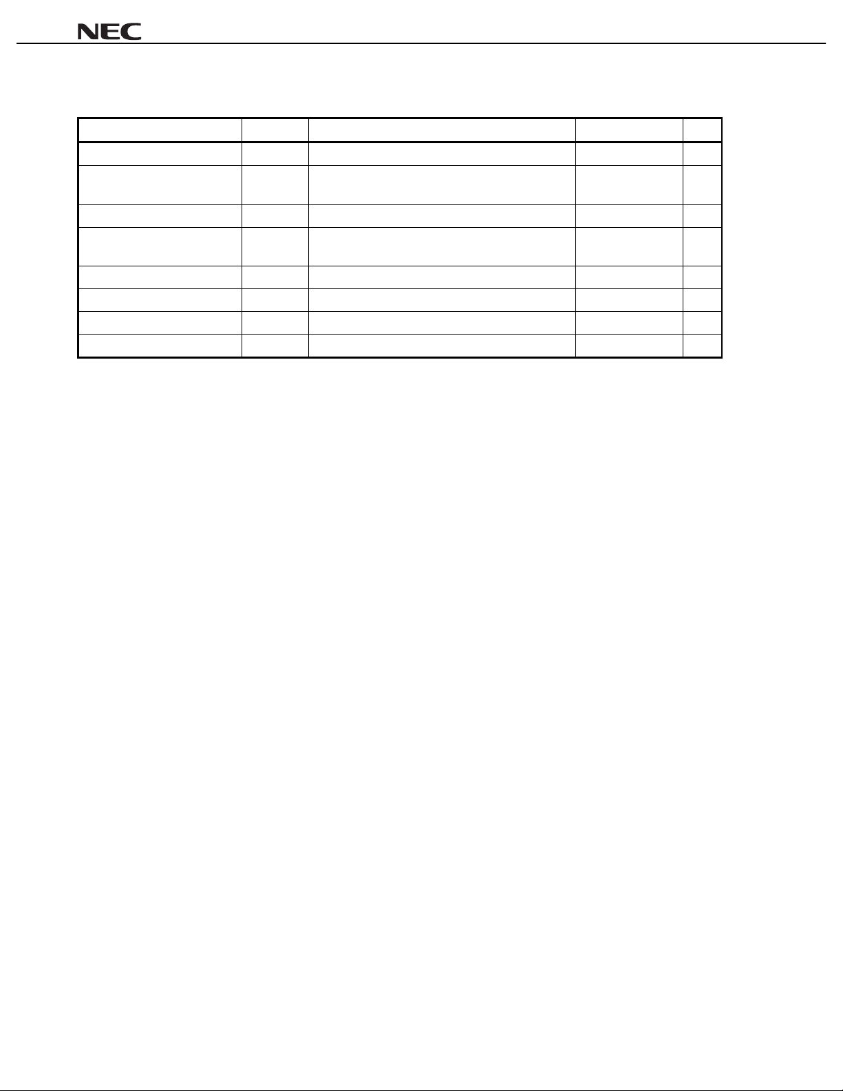
Page 4
µµµµ
PC3205GR
Pin
No.
11 Q OUT 2.6 Q-signal output pi n.
12 GND(PS) 0.0 Ground pin.
13 GND(PS) 0.0 Ground pin.
14 OSC-C2 3.4 Connected capacitor bet ween 14 pi n and 15
15 OSC-B1 3. 0 Connect ed SAW resonator through
Pin
Name
Pin Voltage
TYP. (V)
Function and Explanation Equivalent Circuit
pin to oscillate with active f eedback loop.
capacitor.
14
11
REG
17
16 OSC-B2 3. 0 Connect ed SAW resonator through
capacitor.
17 OSC-C1 3.4 Connected capacitor bet ween 16 pi n and 17
pin to oscillate with active f eedback loop.
18 VCC(PS) 5.0 Supply voltage pin.
19 GND(PS) 0.0 Ground pin.
20 I OUT 2.6 I-signal output pin.
16
15
20
REG
4
Data Sheet P13541EJ3V0DS00
Page 5
ABSOLUTE MAXIMUM RATINGS (TA = +25°C unless otherwise specified)
Parameter Symbol Test Condition Rating Unit
µµµµ
PC3205GR
Supply Voltage V
Power Dissipation P
Operating Ambient Temperature
Storage Temperature T
Mounted on 50 mm × 50 mm × 1.6 mm double epoxy glass board.
Note
CC
TA = +85°C
D
A
T
stg
Note
RECOMMENDED OPERATING RANGE
Parameter Symbol Test Condition MIN. TYP. MAX. Unit
T
AGC
CC
A
IF
V
out
= 1 V
P-P
Supply Voltage V
Operating Ambient Temperature
IF Input Level Range P
Gain Control Voltage Range V
ELECTRICAL CHARACTERISTICS (TA = +25°C, VCC = 5 V, Zin = 50
Parameter Symbol Test Conditions MIN. TYP. MAX. Unit
Circuit Current I
IF Input Frequency f
IQ Output Frequency f
Conversion Gain 1 Gcv1 fIF = 490 MHz, f
Conversion Gain 2 Gcv2
Conversion Gain 3 Gcv3 fIF = 490 MHz, f
AGC Gain Control Range GCR fIF = 490 MHz, f
IQ Phase Balance
IQ Amplitude Balance
Output Voltage V
Maximum Output Voltage Voclip
CC
No input signal 48 65 78 mA
OSC
fIF > f
IF
IQ
Gcv (@fIQ = 10 MHz) ± 1 dB, Vout = 1 V
PIF = –45 to –25 dBm
AGC
V
= 0 to 0.5 V
IF
= 490 MHz, f
f
AGC
V
= 4.5 V to V
AGC
V
= 0.5 to 4.5 V
fIF = 490 MHz, f
φ
∆
PIF = –45 to –25 dBm
VfIF = 490 MHz, f
∆
PIF = –45 to –25 dBm
fIQ = 0.3 to 30 MHz, PIF = –45 to –25 dBm
out
AGC
= 0 to 0.5 V, PIF = –45 to –25 dBm
V
OSC
= 479.5 MHz
OSC
= 479.5 MHz, V
OSC
= 479.5 MHz
CC
OSC
= 479.5 MHz
OSC
= 479.5 MHz, V
OSC
= 479.5 MHz, V
6.0 V
433 mW
–40 to +85 °C
–55 to +150 °C
4.5 5.0 5.5 V
–25 +25 +85 °C
–45 – –25 dBm
0.0 – V
out
, Z
= 1 k
ΩΩΩΩ
)
ΩΩΩΩ
Note
P-P
Note
Note
AGC
= 2 V
Note
Note
Note
out
P-P
= 1 V
Note
P-P
= 1 V
out
Note
Note
Note
CC
V
440 – 520 MHz
0.3 – 30 MHz
49 53 – dB
–44–dB
– – 10 dB
39 – – dB
–2 0 +2 deg
–0.5 0 +0.5 dB
–1.0–V
1.8 – – V
P-P
P-P
By measurement circuit 1
Note
Data Sheet P13541EJ3V0DS00
5
Page 6
µµµµ
PC3205GR
STANDARD CHARACTERISTICS (TA = +25 °C, VCC = 5 V, Zin = 50
Parameter Symbol Test Conditions Reference Value Unit
OSC
= 479.5 MHz, fIQ = 10 MHz, V
Noise Figure (DSB) NF
Third Order Intermodulation
Distortion
LO to IF Isolation Iso(LO-IF)
LO to IQ Isolation Iso(LO-IQ) f = 480 MHz
I to Q Isolation Iso(I-Q)
IF Input Impedance Zin(IF) fIF = 480 MHz 138-j45
IF Input Return Loss RL(IF) fIF = 480 MHz 6 dB
IQ Output Impedance ZO(IQ) fIQ = 0.3 to 30 MHz 25
Notes 1.
By measurement circuit 2
By measurement circuit 1
2.
IM
f
3
fIF1 = 489 MHz, fIF2 = 490 MHz, f
out
V
= 0.708 V
f = 480 MHz, 15 pin or 16 pin to 5 pin
15 pin or 16 pin to 11 pin or 20 pin
f = 10 MHz, 11 pin to 20 pin
P-P
/tone
out
, Z
ΩΩΩΩ
AGC
= 0.5 V
OSC
= 479.5 MHz
= 1 k
)
ΩΩΩΩ
Note 1
Note 2
Note 2
Note 2
Note 2
12.5 dB
56 dBc
50 dB
30 dB
30 dB
Ω
Ω
6
Data Sheet P13541EJ3V0DS00
Page 7

TYPICAL CHARACTERISTICS (TA = +25°C)
µµµµ
PC3205GR
CIRCUIT CURRENT vs. SUPPLY VOLTAGE
80
no input signal
70
60
(mA)
50
CC
(dB)
CV
CONVERSION GAIN vs. AGC VOLTAGE
60
50
40
30
VCC = 4.5 V
VCC = 5.0 V
VCC = 5.5 V
40
20
30
Circuit Current I
20
10
0
1234560
Supply Voltage V
CC
(V)
10
Conversion Gain G
fIF = 490 MHz
0
PIF = −45 dBm
OSC
= 479.5 MHz
f
measurement circuit 1
−10
1234560
AGC V oltage V
AGC
(V)
IQ PHASE BALANCE vs. IQ OUTPUT FREQUENCY IQ AMPLITUDE BALANCE vs. IQ OUTPUT FREQUENCY
93
92
91
φ
VCC = 4.5 V
CC
= 5.0 V
V
VCC = 5.5 V
90
0.5
0.4
0.3
0.2
0.1
0
VCC = 4.5 V
CC
= 5.0 V
V
VCC = 5.5 V
−0.1
IQ Phase Balance ∆ (degree)
89
88
87
f
OSC
= 479.5 MHz
V
out
= 1 V
measurement circuit 1
1 10 1000.1
IQ Output Frequency f
P-P
(1 kΩ)
IQ
(MHz) IQ Output Frequency fIQ (MHz)
−0.2
IQ Amplitude Balance ∆V (dB)IQ Amplitude Balance ∆V (dB)
−0.3
−0.4
−0.5
f
OSC
= 479.5 MHz
V
out
= 1 V
P-P
measurement circuit 1
(1 kΩ)
1 10 1000.1
IQ PHASE BALANCE vs. IF INPUT POWER IQ AMPLITUDE BALANCE vs. IF INPUT POWER
93
92
VCC = 4.5 V
VCC = 5.0 V
CC
= 5.5 V
V
91
φ
90
0.5
0.4
0.3
0.2
0.1
0
VCC = 4.5 V
VCC = 5.0 V
VCC = 5.5 V
−0.1
IQ Phase Balance ∆ (degree)
89
88
87
−40 −30 −10−20−50
IF Intput Power P
fIF = 490 MHz
f
OSC
= 479.5 MHz
out
= 1 V
P-P
V
measurement circuit 1
(1 kΩ)
IF
(dBm) IF Input Power PIF (dBm)
Data Sheet P13541EJ3V0DS00
−0.2
−0.3
−0.4
−0.5
fIF = 490 MHz
f
OSC
= 479.5 MHz
out
= 1 V
V
measurement circuit 1
−40 −30 −10−20−50
P-P
(1 kΩ)
7
Page 8

µµµµ
PC3205GR
IQ OUTPUT POWER vs. IF INPUT POWER
0
1st
2nd
3rd
−20
(50 Ω/1050Ω) (dBm)
−40
out
−60
IQ Output Power P
−80
IQ OUTPUT POWER vs. IF INPUT POWER
0
1st
2nd
3rd
−20
−50 −40 −20−30−60
IF Input Power P
VCC = 5 V
V
AGC
= 0.5 V
fIF = 490 MHz
OSC
= 479.5 MHz
f
measurement circuit 1
IF
(dBm)
IQ OUTPUT POWER vs. IF INPUT POWER
0
1st
2nd
3rd
−20
(50 Ω/1050Ω) (dBm)
−40
out
−60
IQ Output Power P
−80
−50 −40 −20−30
IF Input Power P
IQ OUTPUT POWER vs. IF INPUT POWER
0
VCC = 5 V
AGC
= 3 V
V
fIF = 490 MHz
f
OSC
= 479.5 MHz
measurement circuit 1
−20
VCC = 5 V
V
AGC
= 2 V
IF
= 490 MHz
f
f
OSC
= 479.5 MHz
measurement circuit 1
IF
(dBm)
1st
2nd
3rd
(50 Ω/1050Ω) (dBm)
−40
out
−60
VCC = 5 V
V
AGC
= 2.5 V
IF
= 490 MHz
f
f
OSC
IQ Output Power P
−80
−20
(50 Ω/1050Ω) (dBm)
−40
out
= 479.5 MHz
measurement circuit 1
IQ OUTPUT POWER vs. IF INPUT POWER
0
VCC = 5 V
AGC
= 3.5 V
V
fIF = 490 MHz
f
OSC
= 479.5 MHz
measurement circuit 1
−60
IQ Output Power P
−80
−30 −10−20−40
IF Input Power P
−20 0−10−30
IF Input Power P
IF
(dBm)
IF
(dBm)
1st
2nd
3rd
(50 Ω/1050Ω) (dBm)
−40
out
−60
IQ Output Power P
−80
−30 −20 0−10
IF
IF Input Power P
IQ MAXIMUM OUTPUT VOLTAGE vs. AGC VOLTAGE
3
)
P-P
2.5
(dBm)
VCC = 4.5 V
VCC = 5 V
CC
= 5.5 V
V
2
1.5
1
0.5
fIF = 490 MHz
IQ Maximum Output Voltage Voclip (V
f
OSC
= 479.5 MHz
measurement circuit 1
0
01 5234
AGC
AGC Voltage V
(V)
8
Data Sheet P13541EJ3V0DS00
Page 9

STANDARD CHARACTERISTICS (TA = +25°C)
THIRD ORDER INTERMODULATION DISTORTION
60
50
40
(dBc)
3
OUTPUT)
30
p-p
fIF1 = 489 MHz
fIF2 = 490 MHz
f
OSC
20
Distortion IM
(2tone 1V
Third Order Intermodulation
10
= 479.5 MHz
V
out
= 0.708 V
/tone (1 kΩ)
measurement circuit 1
V
CC
= 4.5 V
VCC = 5.0 V
0
VCC = 5.5 V
−40 −30 −10−20−50
IF Input Power P
P-P
IF
/tone (dBm)
µµµµ
PC3205GR
2nd/3rd ORDER INTERMODULATION DISTORTION
0
−10
1st
−20
−30
−40
(50 Ω/1050Ω) (dBm)
out
−50
3rd
2nd
−60
VCC = 5 V
−70
−80
IQ Output Power P
−90
−50 −40 −30−60
IF Input Power P
fIF1 = 489 MHz
fIF2 = 490 MHz
f
OSC
= 479.5 MHz
V
AGC
= 0.5 V
measurement circuit 1
IF
/tone (dBm)
2nd/3rd ORDER INTERMODULATION DISTORTION
0
−10
1st
−20
−30
−40
(50 Ω/1050Ω) (dBm)
out
−50
3rd
2nd
−60
VCC = 5 V
−70
−80
IQ Output Power P
−90
−30 −20 −10−40
IF Input Power P
fIF1 = 489 MHz
fIF2 = 490 MHz
f
OSC
= 479.5 MHz
V
AGC
= 2.5 V
measurement circuit 1
IF
/tone (dBm)
Data Sheet P13541EJ3V0DS00
9
Page 10

STANDARD CHARACTERISTICS
IF INPUT IMPEDANCE
MARKER 1
480 MHz
138.35 Ω –45.359 Ω
µµµµ
PC3205GR
1
START 10.000 000 MHz STOP 1000.000 000 MHz
IQ OUTPUT IMPEDANCE
MARKER 1
10 MHz
25.26 Ω 1.845 Ω
1
10
START .300 000 MHz STOP 100.000 000 MHz
Data Sheet P13541EJ3V0DS00
Page 11

THERMAL CHARACTERISTICS (FOR REFERENCE)
CIRCUIT CURRENT vs. SUPPLY VOLTAGE
80
no input signal
70
CONVERSION GAIN vs. AGC VOLTAGE
60
50
µµµµ
PC3205GR
TA = −25 °C
TA = +25 °C
TA = +85 °C
60
(mA)
50
CC
40
(dB)
CV
30
40
20
30
Circuit Current I
20
10
0
1234560
Supply Voltage V
TA = −25 °C
T
TA = +85 °C
CC
(V)
A
= +25 °C
10
Conversion Gain G
VCC = 5 V
fIF = 490 MHz
0
PIF = −45 dBm
f
OSC
= 479.5 MHz
measurement circuit 1
−10
1234560
AGC V oltage V
AGC
(V)
IQ PHASE BALANCE vs. IQ OUTPUT FREQUENCY IQ AMPLITUDE BALANCE vs. IQ OUTPUT FREQUENCY
92
TA = −25 °C
TA = +25 °C
TA = +85 °C
91
φ
90
0.5
0.4
TA = −25 °C
TA = +25 °C
TA = +85 °C
0.3
0.2
φ
0.1
0
−0.1
−0.2
89
IQ Phase Balance ∆ (degree)
88
VCC = 5 V
f
OSC
= 479.5 MHz
V
out
= 1 V
P-P
measurement circuit 1
(1 kΩ)
1 10 1000.1
IQ Amplitude Balance ∆ (dB)IQ Amplitude Balance ∆ (dB)
−0.3
−0.4
−0.5
VCC = 5 V
f
OSC
= 479.5 MHz
V
out
= 1 V
P-P
measurement circuit 1
(1 kΩ)
1 10 1000.1
IQ Output Frequency fIQ (MHz) IQ Output Frequency fIQ (MHz)
IQ PHASE BALANCE vs. IF INPUT POWER IQ AMPLITUDE BALANCE vs. IF INPUT POWER
93
92
TA = −25 °C
TA = +25 °C
TA = +85 °C
91
φ
90
0.5
0.4
TA = −25 °C
TA = +25 °C
TA = +85 °C
0.3
φ
0.2
0.1
0
−0.1
IQ Phase Balance ∆ (degree)
89
88
87
VCC = 5 V
fIF = 490 MHz
f
OSC
= 479.5 MHz
V
out
= 1 V
P-P
measurement circuit 1
(1 kΩ)
−40 −30 −10−20−50
−0.2
−0.3
−0.4
−0.5
VCC = 5 V
fIF = 490 MHz
f
OSC
= 479.5 MHz
V
out
= 1 V
measurement circuit 1
−40 −30 −10−20−50
IF Intput Power PIF (dBm) IF Input Power PIF (dBm)
Data Sheet P13541EJ3V0DS00
P-P
(1 kΩ)
11
Page 12

µµµµ
PC3205GR
IQ OUTPUT POWER vs. IQ OUTPUT FREQUENCY
−20
−22
−24
(50 Ω/1050Ω) (dBm)
out
VCC = 5 V
−26
f
OSC
= 479.5 MHz
V
AGC
= 0.5 V
PIF = −50 dBm
V
out
= 1 V
P-P
−28
measurement circuit 1
IQ Output Power P
−30
(1 kΩ)
TA = −25 °C
TA = +25 °C
TA = +85 °C
1 10 1000.1
IQ Output Frequency f
IQ
(MHz)
2nd/3rd ORDER INTERMODULATION DISTORTION
0
−10
−20
1st
3rd ORDER INTERMODULATION DISTORTION
60
(dBc)
3
50
40
OUTPUT)
P-P
30
VCC = 5 V
fIF1 = 489 MHz
fIF2 = 490 MHz
f
OSC
20
(2tone 1V
10
Third Order Intermodulation Distortion IM
= 479.5 MHz
V
out
= 0.708 V
/tone (1 kΩ)
measurement circuit 1
TA = −25 °C
TA = +25 °C
0
TA = +85 °C
−40 −30 −10−20−50
IF Input Power P
P-P
IF
/tone (dBm)
2nd/3rd ORDER INTERMODULATION DISTORTION
0
−10
−20
1st
−30
−40
(50 Ω/1050 Ω) (dBm)
out
−50
−60
−70
−80
IQ Output Power P
−90
IF Input Power P
3rd
2nd
TA = −25 °C
V
CC
= 5 V
fIF1 = 489 MHz
fIF2 = 490 MHz
f
OSC
= 479.5 MHz
V
AGC
= 0.5 V
measurement
circuit 1
−50 −40 −30−60
IF
/tone (dBm)
2nd/3rd ORDER INTERMODULATION DISTORTION
0
−10
−20
1st
−30
−40
(50 Ω/1050 Ω) (dBm)
out
−50
−60
−70
−80
IQ Output Power P
−90
IF Input Power P
3rd
2nd
TA = −25 °C
VCC = 5 V
fIF1 = 489 MHz
fIF2 = 490 MHz
f
OSC
= 479.5 MHz
V
AGC
= 2.5 V
measurement
circuit 1
−30 −20 −10−40
IF
/tone (dBm)
−30
−40
(50 Ω/1050 Ω) (dBm)
out
−50
−60
−70
−80
IQ Output Power P
−90
IF Input Power P
3rd
2nd
TA = +85 °C
V
CC
= 5 V
fIF1 = 489 MHz
fIF2 = 490 MHz
f
OSC
= 479.5 MHz
V
AGC
= 0.5 V
measurement
circuit 1
−50 −40 −30−60
IF
/tone (dBm)
2nd/3rd ORDER INTERMODULATION DISTORTION
0
−10
−20
1st
−30
−40
(50 Ω/1050 Ω) (dBm)
out
−50
−60
−70
−80
IQ Output Power P
−90
IF Input Power P
3rd
2nd
TA = +85 °C
VCC = 5 V
fIF1 = 489 MHz
fIF2 = 490 MHz
f
OSC
= 479.5 MHz
V
AGC
= 2.5 V
measurement
circuit 1
−30 −20 −10−40
IF
/tone (dBm)
12
Data Sheet P13541EJ3V0DS00
Page 13

MEASUREMENT CIRCUIT 1
µ
VCC
VAGC
IF 1
IF IN
50 Ω
IF 2
*1
1 F
1 000 pF
1 000 pF
1 000 pF
1 F
1 F
µ
µµµµ
PC3205GR
1
2
3
4
5
6
7
8
µ
9
10
IF
Amplifier
AGC
Amplifier
MIXER
90 deg
phase
shifter
0°
90°
LPF
LPF
OSC
20
µ
1 F
19
18
17
16
15
14
13
12
11
1 F
1 pF
100 pF
1 pF
(MURATA:
SAR479.45MB10×200)
µ
1 F 1 kΩ Q OUT
1 kΩ I OUT
µ
100 pF
SAW Resonator
50 Ω
*2
3
In the case of measurement of IM
*1
• Vector Signal Analyzer or Vector Voltage Meter @measurement of IQ phase balance and IQ amplitude
*2
.
balance.
• Spectrum Analyzer @measurement of bandwidth and IM3.
MEASUREMENT CIRCUIT 2
NF
Meter
µ
V
V
Noise
Source
CC
AGC
IF IN
1 F
1 000 pF
1 000 pF
1 000 pF
1 F
1
2
3
4
5
6
AGC
IF
Amplifier
7
Amplifier
8
µ
1 F
9
10
µ
MIXER
90 deg
phase
shifter
0°
90°
LPF
LPF
OSC
20
19
18
17
16
15
14
13
12
11
µ
1 kΩ
1 F
µ
1 F
I OUT
1 pF
100 pF
100 pF
1 pF
SAW Resonator
(MURATA:
SAR479.45MB10×200)
Q OUT
µ
1 kΩ
1 F
LPF
LPF
Data Sheet P13541EJ3V0DS00
13
Page 14

APPLICATION CIRCUIT EXAMPLE (In the case of LO single input)
µµµµ
PC3205GR
µ
V
CC
V
AGC
IF IN
The application circuits and their parameters are for reference only and are not intended for use in actual design-ins.
1 F
1 000 pF
1 000 pF
1 000 pF
1 F
µ
µ
1 F
1
2
3
4
5
6
7
8
9
10
IF
Amplifier
AGC
Amplifier
MIXER
90 deg
phase
shifter
0°
90°
LPF
LPF
OSC
20
19
18
17
16
15
14
13
12
11
µ
1 F
1 000 pF
1 000 pF
µ
1 F
µ
1 F
I OUT
1 kΩ
LO IN
56 Ω
Q OUT
1 kΩ
14
Data Sheet P13541EJ3V0DS00
Page 15

PACKAGE DIMENSIONS
20 PIN PLASTIC SSOP (225 mil) (UNIT: mm)
µµµµ
PC3205GR
20
110
6.7 ± 0.3
1.8 MAX.
1.5 ± 0.1
11
detail of lead end
3˚
6.4 ± 0.2
4.4 ± 0.1
+7˚
–3˚
1.0 ± 0.2
NOTE
0.5 ± 0.2
0.15
+0.10
–0.05
0.1 ± 0.1
0.65
0.22
+0.10
–0.05
0.10
0.15
M
0.575 MAX.
Each lead centerline is located within 0.10 mm of its true position (T.P.) at maximum material condition.
Data Sheet P13541EJ3V0DS00
15
Page 16

µµµµ
PC3205GR
NOTE ON CORRECT USE
(1) Observe precautions for handling because of electro-static sensitive devices.
(2) Form a ground pattern as widely as possible to minimize ground impedance (to prevent undesires oscillation).
(3) Keep the track length of the ground pins as short as possible.
(4) A low pass filter must be attached to Vcc line.
RECOMMENDED SOLDERING CONDITIONS
This product should be soldered under the following recommended conditions. For soldering methods and
conditions other than those recommended below, contact your NEC sales representative.
Soldering Method Soldering Conditions
Infrared Reflow Package peak temperature: 235 ° C or bel ow
Time: 30 seconds or less (at 210 °C)
Count: 3, Exposure limi t
VPS Package peak temperature: 215 °C or below
Time: 40 seconds or less (at 200 °C)
Count: 3, Exposure limi t
Wave soldering Soldering bath temperature: 260 °C or bel ow
Time: 10 seconds or less
Count: 1, Exposure limi t
Partial Heating Pin temperature: 300 °C
Time: 3 seconds or less (per side of device)
Exposure limit
After opening the dry pack, keep it in a place below 25 °C and 65% RH for the allowable storage period.
Note
Note
: None
Note
Note
Note
: None
: None
: None
Recommended Condition
Symbol
IR35-00-3
VP15-00-3
WS60-00-1
−
Caution Do not use different soldering methods together (except for partial heating).
For details of recommended soldering conditions for surface mounting, refer to information document
SEMICONDUCTOR DEVICE MOUNTING TECHNOLOGY MANUAL (C10535E).
16
Data Sheet P13541EJ3V0DS00
Page 17

[MEMO]
µµµµ
PC3205GR
Data Sheet P13541EJ3V0DS00
17
Page 18

[MEMO]
µµµµ
PC3205GR
18
Data Sheet P13541EJ3V0DS00
Page 19

[MEMO]
µµµµ
PC3205GR
Data Sheet P13541EJ3V0DS00
19
Page 20

µµµµ
PC3205GR
• The information in this document is subject to change without notice. Before using this document, please
confirm that this is the latest version.
• No part of this document may be copied or reproduced in any form or by any means without the prior written
consent of NEC Corporation. NEC Corporation assumes no responsibility for any errors which may appear in
this document.
• NEC Corporation does not assume any liability for infringement of patents, copyrights or other intellectual property
rights of third parties by or arising from use of a device described herein or any other liability arising from use
of such device. No license, either express, implied or otherwise, is granted under any patents, copyrights or other
intellectual property rights of NEC Corporation or others.
• Descriptions of circuits, software, and other related information in this document are provided for illustrative
purposes in semiconductor product operation and application examples. The incorporation of these circuits,
software, and information in the design of the customer's equipment shall be done under the full responsibility
of the customer. NEC Corporation assumes no responsibility for any losses incurred by the customer or third
parties arising from the use of these circuits, software, and information.
• While NEC Corporation has been making continuous effort to enhance the reliability of its semiconductor devices,
the possibility of defects cannot be eliminated entirely. To minimize risks of damage or injury to persons or
property arising from a defect in an NEC semiconductor device, customers must incorporate sufficient safety
measures in its design, such as redundancy, fire-containment, and anti-failure features.
• NEC devices are classified into the following three quality grades:
"Standard", "Special", and "Specific". The Specific quality grade applies only to devices developed based on a
customer designated "quality assurance program" for a specific application. The recommended applications of
a device depend on its quality grade, as indicated below. Customers must check the quality grade of each device
before using it in a particular application.
Standard: Computers, office equipment, communications equipment, test and measurement equipment,
audio and visual equipment, home electronic appliances, machine tools, personal electronic
equipment and industrial robots
Special: Transportation equipment (automobiles, trains, ships, etc.), traffic control systems, anti-disaster
systems, anti-crime systems, safety equipment and medical equipment (not specifically designed
for life support)
Specific: Aircraft, aerospace equipment, submersible repeaters, nuclear reactor control systems, life
support systems or medical equipment for life support, etc.
The quality grade of NEC devices is "Standard" unless otherwise specified in NEC's Data Sheets or Data Books.
If customers intend to use NEC devices for applications other than those specified for Standard quality grade,
they should contact an NEC sales representative in advance.
M7 98. 8
 Loading...