

Page 1
DATA SHEET
BIPOLAR ANALOG INTEGRATED CI RCUT
µµµµ
PC305
POSITIVE VOLTAGE STABILIZED POWER SUPPLY
DESCRIPTION
The µPC305 is a high-performance stabilized power supply that can supply a constant voltage in a wide
temperature range even if the input voltage or load voltage fluctuates, by integrating a high-gain error amplifier and a
temperature-compensating constant-voltage diode on a single chip.
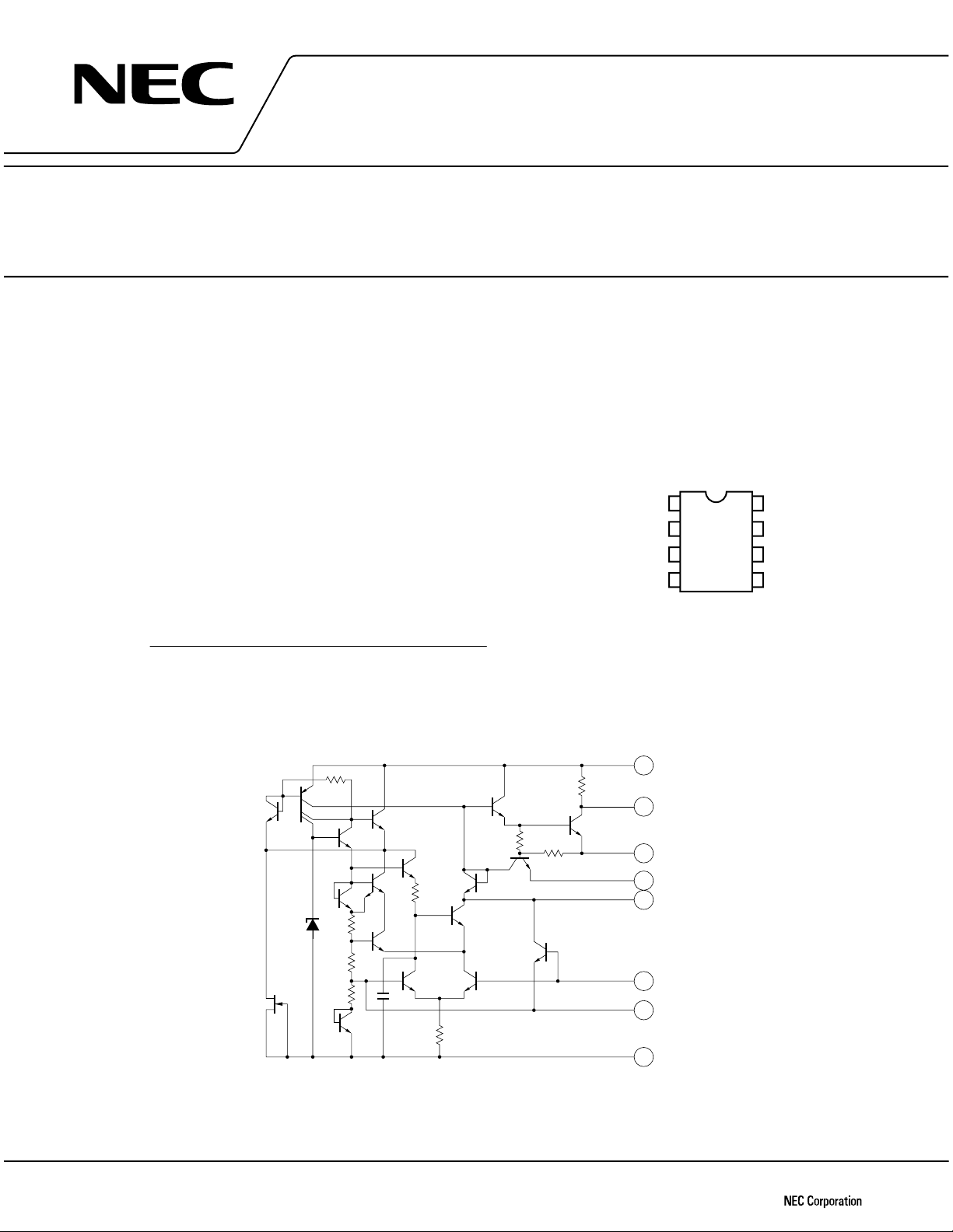
FEATURES PIN CONFIGURATION (Top View)
Wide output voltage variable range Vo: 4.5 to 30 V, V
•
Excellent load stability 0.02%
•
Good ripple rejection ratio 0.003%/V
•
DIF
: 3 to 30 V
Current limiter
Current output
Input
GND
µ
PC305C, 305G2
1
2
3
4
8
7
6
5
Output
Compensation
Error detection
Reference voltage
ORDERING INFORMATION
Part Number Package
PC305C 8-pin plastic DIP (7.62 mm (300))
µ
PC305G2 8-pin plastic SOP (5.72 mm (225))
µ
EQUIVALENT CIRCUIT
R
7
2.8 kΩ
Q
Q
11
12
Q
13
Q
10
Q
9
Q
7
6
Q
8
R
4
1
D
3 kΩ
R
3
6.8 k
Ω
R
3 kΩ
2
Q
1
Q
18
R
4.4 kΩ
Q
Q
4
2
Q
1
C
5 pF
R
5
2.2 kΩ
1.86 kΩ
6
Q
5
Q
3
Input
R
9
R
1.32 kΩ
600 Ω
Q
15
Q
14
R
8
Q
16
Q
17
3
10
Current output
2
Current limiter
1
Output
8
Compensation
7
Error detection
6
Reference voltage
5
GND
4
The information in this document is subject to change without notice. Before using this document, please
confirm that this is the latest version.
Not all devices/types available in every country. Please check with local NEC representative for
availability and additional information.
Document No. G10633EJ3V0DS00 (3rd edition)
Date Published December 1999 N CP(K)
Printed in Japan
©
1999
Page 2
µµµµ
PC305
ABSOLUTE MAXIMUM RATINGS (Unless otherwise specified, TA = 25
Parameter Symbol
Input Voltage V
Input − Output Voltage Difference V
Maximum Output Current I
Total Loss P
Operating Temperature T
Storage Temperature T
A
Notes 1.
Where T
Where TA > +25°C, perform derating at TJ MAX. 125°C, −4.4 mW/°C.
2.
> +55°C, perform derating at TJ MAX. 125°C, −5 mW/°C.
IN
DIF
O
T
A
stg
PC305C
µ
350
Note 1
0.3 to +40 V
−
40 V
50 mA
0 to +70
55 to +125
−
C)
°°°°
PC305G2 Unit
µ
Note 2
440
mW
C
°
C
°
Caution If any of the parameters exceeds the absolute maximum ratings, even momentarily, the quality of
the product may be impaired. The absolute maximum ratings are values that may physically
damage the product(s). Be sure to use the product(s) within the ratings.
ELECTRICAL SPECIFICATIONS (Unless otherwise specified, TA = 25
Parameter Symbol Condition MIN. TYP. MAX. Unit
Input Voltage Range V
Output Voltage Range V
Input − Output Voltage Difference V
Load Stability REG
Ripple Rejection Ratio REJ C
Temperature Stability 0°C ≤ TA ≤ 70°C0.31.0%
Reference Voltage V
Long-time Stability 0.1 %
Supply Current under No Load I
IN
OUT
DIF
L
0 ≤ IO ≤ 12 mA, RSC = 18
IN
REF
N
CC
OUT
VIN – V
VIN – V
≤ 5 V 0.025 0.06 %/VInput Stability REG
OUT
> 5 V 0.015 0.03 %/V
REF
= 10 µF, f = 120 Hz 0.003 %/V
10 Hz ≤ f ≤ 10 kHz, C
REF
C
= 0.1 µF 0.002 %
VIN = 40 V 1.0 2.0 mA
REF
Ω
= 0 µF 0.005 %Output Noise Voltage V
C)
°°°°
8.0 40 V
4.5 30 V
3.0 30 V
0.02 0.05 %
1.65 1.8 1.90 V
Remark
2
SC
: Current-limiting resistor
R
REF
C
: Bypass capacitor of reference voltage pin
Data Sheet G10633EJ3V0DS00
Page 3
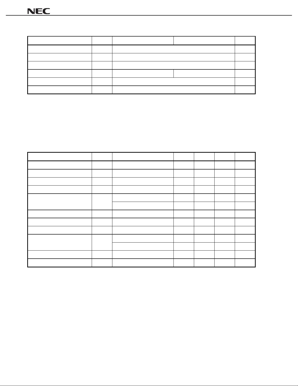
STANDARD CHARACTERISTIC CURVES
= 25
(Unless otherwise specified, T
A
C. Reference values)
°°°°
µµµµ
PC305
500
400
300
[mW]
T
200
Total Loss P
100
0
0
−0.02
−0.04
PT vs TA Characteristics
µ
PC305G
µ
PC305C
Operating Temperature TA [°C]
Load Stability (2)
TA = 0°C
TA = 25°C
Load Stability (1)
0
−0.01
−0.02
−0.03
Output Voltage Fluctuation (%)
−0.04
100
RSC = 0 Ω
0100806040200 51015
80
60
TA = 0°C
Output Current I
Current-limiting Characteristics
TA = +70°C
A
= +70°C
T
TA = −20°C
O
(mA)
TA = 0°C
TA = 25°C
−0.06
Outout Voltage Fluctuation (%)
−0.08
−0.1
0 102030
3.0
2.8
2.6
Resistance (kΩ)
2
2.4
R
2.2
2.0
51020
TA = +70°C
RSC = 13 Ω
Output Current I
Resistance for Setting Output Voltage
Output Voltage (V)
O
(mA)
R1//R2 = 2 kΩ
R1 = 1110×V
R
2
TA = −20°C
Output Voltage Drop Ratio (%)
40
OUT
(Ω)
Pickup Voltage Across Pins <1> and <8> (V)
50 0806020
TA = −20°C
40
20
RSC = 13 Ω
0
050
0.63.2
0.5
0.4
0.3
0.2
10 20 30 40
Output Current I
Current-limiting Pickup Voltage
Operating Temperature T
40
O
(mA)
A
(°C)
Data Sheet G10633EJ3V0DS00
3
Page 4

µµµµ
PC305
Line Regulation
0.1
0.05
0.02
0.01
0.005
ref
= 10 F
f≤120 Hz
µ
520
0.002
Output Voltage Fuctuation Ratio (%)
0.001
C
1102
Input - Output Voltage Difference V
APPLICATION CIRCUIT EXAMPLES
5 V-15 mA Regulator
V
OUT
A
= 25°C
T
C
ref
= 10 V
= 0 F
DIF
(V)
Transient Response Time
40
0
µ
−40
LINE
CL = 0
CL = 1 F
LOAD
µ
50
400
0
Output Voltage Fluctuation (mV)
−400
01020
Response Time ( s)
V
OUT
µ
RSC = 10 Ω
IN
= 5 V
∆V
= 10 V
RSC = 10 Ω
FL
= 20 mA
I
NL
= 1.0 mA
I
OUT
= 10 V
V
30
10 V-200 mA Regulator (Drooping Characteristics)
R3 13 Ω
8
1
47 pF
V
IN
≥ 8 V
1
2
3
C
3
µ
0.01 F
C
7
6
3.1 kΩ
5
4
C
10 F
REF
1
R
5.6 kΩ
R
2
µ
15 V-1A Regulator (Fold-back Characteristics)
R
3
1.3 Ω 2 W
+
C
−
2SD297
IN
≥ 19 V
V
4
1 F
µ
R
6
2SB505
C
3
µ
0.1 F
R
130 Ω
3
110 Ω
1
2
3
R
5
1.2 kΩ
C
1
47 pF
8
7
R
16.7
kΩ
6
5
4
C
REF
10 F
µ
R
2.3
kΩ
+
−
C
2
µ
1 F
V
O
= 5 V
V
IN
2SB505
≥ 13 V
R3 1.3 Ω 0.5 W
1
2
3
C
3
µ
0.01 F
1
47 pF
C
8
7
5
4
6
C
REF
10 F
µ
R
1
11.2 kΩ2.45 kΩ
R
2
+
C
−
3.3 F
V
O
= 10 V
2
µ
1A Constant-current Regulator
IN
O
= 15 V
V
1
+
C
2
−
µ
50 F
2
8
1
2
3
4
680 Ω
7
C
47 pF
6
5
2SD79
R
4
1
R
3
R
2
68 Ω
2 kΩ
R
1
1.8 Ω 2W
Load
V
2SD73
Caution Note the power consumption of the
external transistor.
4
PC305 when the output pin is short-circuited and that of the
µµµµ
Data Sheet G10633EJ3V0DS00
Page 5

PACKAGE DRAWINGS
8-PIN PLASTIC DIP (7.62mm(300))
85
14
A
J
I
µµµµ
PC305
K
P
L
H
G
C
B
F
DN
NOTES
1. Each lead centerline is located within 0.25 mm of
its true position (T.P.) at maximum material condition.
2. ltem "K" to center of leads when formed parallel.
M
M
R
ITEM MILLIMETERS
A 10.16 MAX.
B 1.27 MAX.
C 2.54 (T.P.)
D 0.50±0.10
F 1.4 MIN.
G 3.2±0.3
H 0.51 MIN.
I 4.31 MAX.
J 5.08 MAX.
K 7.62 (T.P.)
L 6.4
M 0.25
N 0.25
P 0.9 MIN.
R0∼15°
+0.10
−0.05
P8C-100-300B,C-2
Data Sheet G10633EJ3V0DS00
5
Page 6

8-PIN PLASTIC SOP (5.72 mm (225))
85
detail of lead end
P
µµµµ
PC305
1
4
A
F
G
S
B
C
D
M
M
E
NOTE
Each lead centerline is located within 0.12 mm of
its true position (T.P.) at maximum material condition.
H
I
J
L
K
ITEM
A 5.2
B
C
D
E
F
G
H
I
J
K
L
M
N
P
SN
MILLIMETERS
+0.17
−0.20
0.78 MAX.
1.27 (T.P.)
+0.08
0.42
−0.07
0.1±0.1
1.59±0.21
1.49
6.5±0.3
4.4±0.15
1.1±0.2
+0.08
0.17
−0.07
0.6±0.2
0.12
0.10
+7°
3°
−3°
S8GM-50-225B-6
6
Data Sheet G10633EJ3V0DS00
Page 7

µµµµ
PC305
RECOMMENDED SOLDERING CONDITIONS
Solder this product under the following recommended conditions.
For details of the recommended soldering conditions, refer to information document
Mounting Technology Manual (C10535E)
.
For soldering methods and conditions other than those recommended, consult NEC.
Surface Mount Type
PC305G2: 8-pin plastic SOP (5.72 mm (225))
µµµµ
Soldering Method Soldering Conditions Recommended
Semiconductor Device
Conditions Symbol
Infrared reflow Package peak temperature: 230°C, Time: 30 sec max. (210°C min.),
Number of times: once
VPS Package peak temperature: 215°C, Time: 40 sec max. (200°C min.),
Number of times: once
Wave soldering Solder bath temperature: 260°C max., Time: 10 sec max., Number of times: once,
Preheating temperature: 120°C max. (Package surface temperature)
IR30-00-1
VP15-00-1
WS60-00-1
Caution Do not use two or more soldering methods in combination (except partial heating).
Through Hole type
PC305C: 8-pin plastic DIP (7.62 mm (300))
µµµµ
Soldering Method Soldering Conditions Recommended
Conditions Symbol
Wave soldering Solder bath temperature: 260°C max., Time: 10 sec max.
Data Sheet G10633EJ3V0DS00
7
Page 8

µµµµ
PC305
• The information in this document is subject to change without notice. Before using this document, please
confirm that this is the latest version.
• No part of this document may be copied or reproduced in any form or by any means without the prior written
consent of NEC Corporation. NEC Corporation assumes no responsibility for any errors which may appear in
this document.
• NEC Corporation does not assume any liability for infringement of patents, copyrights or other intellectual property
rights of third parties by or arising from use of a device described herein or any other liability arising from use
of such device. No license, either express, implied or otherwise, is granted under any patents, copyrights or other
intellectual property rights of NEC Corporation or others.
• Descriptions of circuits, software, and other related information in this document are provided for illustrative
purposes in semiconductor product operation and application examples. The incorporation of these circuits,
software, and information in the design of the customer's equipment shall be done under the full responsibility
of the customer. NEC Corporation assumes no responsibility for any losses incurred by the customer or third
parties arising from the use of these circuits, software, and information.
• While NEC Corporation has been making continuous effort to enhance the reliability of its semiconductor devices,
the possibility of defects cannot be eliminated entirely. To minimize risks of damage or injury to persons or
property arising from a defect in an NEC semiconductor device, customers must incorporate sufficient safety
measures in its design, such as redundancy, fire-containment, and anti-failure features.
• NEC devices are classified into the following three quality grades:
"Standard", "Special", and "Specific". The Specific quality grade applies only to devices developed based on a
customer designated "quality assurance program" for a specific application. The recommended applications of
a device depend on its quality grade, as indicated below. Customers must check the quality grade of each device
before using it in a particular application.
Standard: Computers, office equipment, communications equipment, test and measurement equipment,
audio and visual equipment, home electronic appliances, machine tools, personal electronic
equipment and industrial robots
Special: Transportation equipment (automobiles, trains, ships, etc.), traffic control systems, anti-disaster
systems, anti-crime systems, safety equipment and medical equipment (not specifically designed
for life support)
Specific: Aircraft, aerospace equipment, submersible repeaters, nuclear reactor control systems, life
support systems or medical equipment for life support, etc.
The quality grade of NEC devices is "Standard" unless otherwise specified in NEC's Data Sheets or Data Books.
If customers intend to use NEC devices for applications other than those specified for Standard quality grade,
they should contact an NEC sales representative in advance.
M7 98. 8
 Loading...