

Page 1
uP7534
A
www.DataSheet.co.kr
Datasheet pdf - http://www.DataSheet4U.net/
Current-Limited, Power Distribution Switches
General Description
The uP7534 is a current limited high-side switch designed
for applications where heavy capacitive loads and shortcircuits are likely to be met. This device operates with
inputs from 2.7V to 5.5V for both 3V and 5V systems. Its
low quiescent current (25uA) and standby current (<1uA)
conserve battery power in portable.
The power switch is controlled by a logic enable input and
driven by an internal charge pump circuit. When the output
load exceeds the current-limit threshold or a short is
present, the uP7534 asserts overcurrent protection and
limits the output current to a safe level by driving the power
switch into saturation mode.
The uP7534 features glitch-blank fault flag that is asserted
by overcurrent, overtemperature, or input undervoltage
lockout. The 8ms glitch-blanking time allows momentary
faults to be ignored, thus preventing false alarms to the
host system.
Other features include soft-start to limit inrush current
during plug-in, thermal shutdown to prevent catastrophic
switch failure from high-current loads, under-voltage lockout
(UVLO) to ensure that the device remains off unless there
is a valid input voltage present. The uP7534 is available in
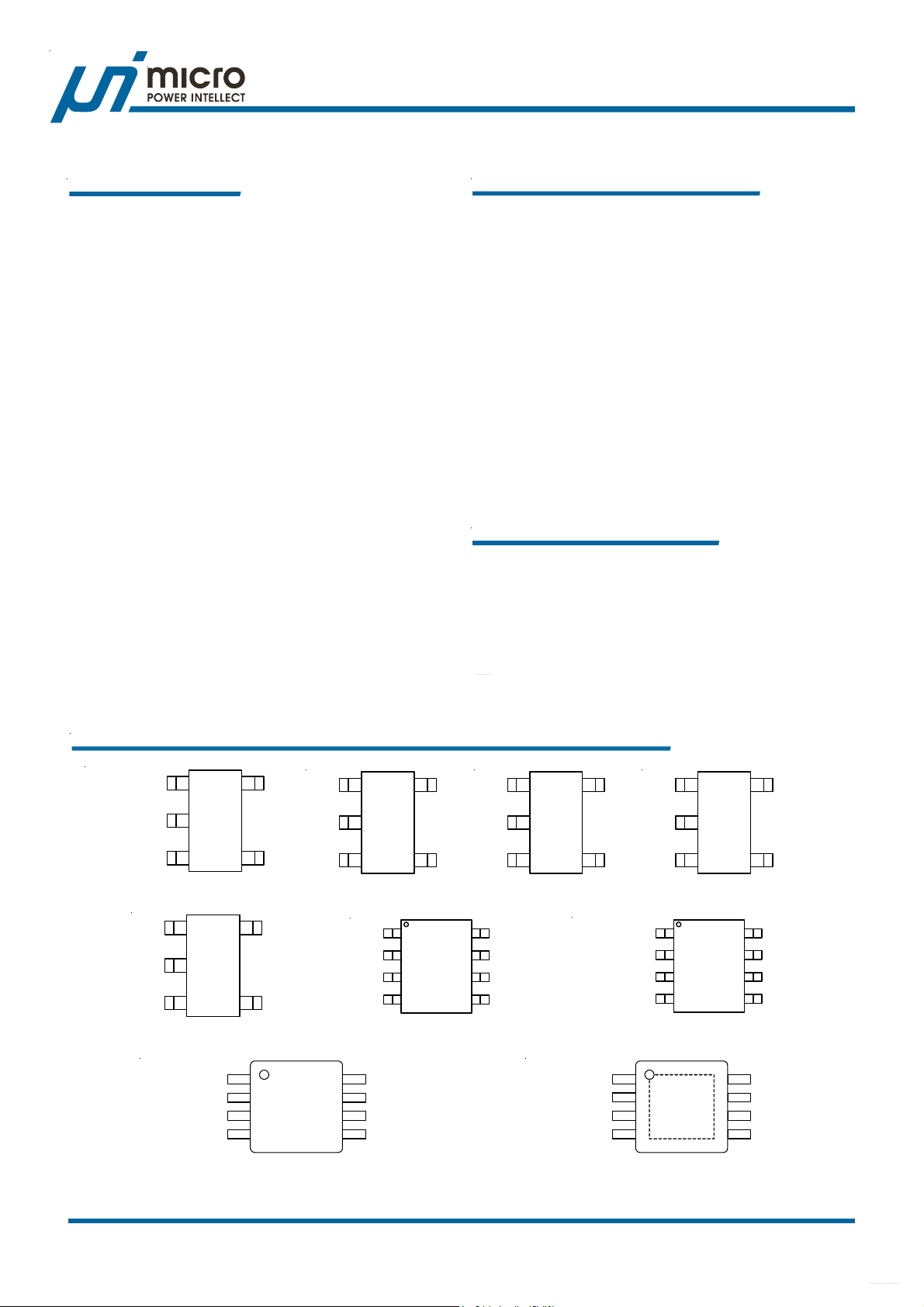
SOP-8 , SOT23-5, MSOP-8, and PMSOP-8 packages.
Compliant to USB Specifications
Operating Range: 2.7 V to 5.5 V
90m
25uA Typical Quiescent Current
<1uA Typical Shutdown Current
Over Current/ Short Circuit Protect
Thermal Shutdown Protection
Deglitched Open Drain Fault Flag
Slow Turn On and Fast Turn Off
Enable Active-High or Active-Low
Pb-Free (RoHS Compliant)
UL Approved-E316940
TuV EN60960-1 Certification
ΩΩ
Ω (5V Input) High Side MOSFET Switch
ΩΩ
pplications
Notebook and Desktop PCs
USB Power Management
ACPI Power Distribution
Hot-Plug Power Supplies
Battery-Powered Equipments
Battery-Charger Circuits
Features
GND
(uP7534C) EN
(uP7534D) EN#
GND
2
3
SOT23-5 (MA5)
2
3OC#
SOT23-5 (MA5)
GND
VIN
VIN
(uP7534A) EN
(uP7534B) EN#
VOUTOC# 1
5
uP7534C/D
VIN
4
VINVOUT 1
5
uP7534G/H
EN(uP7534G)
4
EN#(uP7534H)
1
2
3
4 5
MSOP-8 (RA8)
GND
uP7534A
2
3VIN
SOT23-5 (M5)
OC#
VOUT
VOUT
GND
8
VOUT
VOUT
7
VOUT
6
OC#
5
VOUTVOUT 1
GND
4
EN
1
2
3
45
SOP-8 (S8)
8
7
6
NC
VIN
VIN
EN (uP7534A)
EN# (uP7534B)
uP7534A/B
5
uP7534B
2
4
3VIN
SOT23-5 (M5)
(uP7534A) EN
(uP7534B) EN#
VOUTVOUT 1
VIN
(uP7534C) EN
(uP7534D) EN#
GND
1
VIN
2
VIN
3
4 5
Pin Configuration
5
uP7534E /F
GND
VIN
VIN
}
PMSOP-8 (RU8)
2
4
3NC
SOT23-5 (MA5)
1
2
3
45
SOP-8 (SA8)
GND
8
uP7534C/D
7
6
8
VOUT
VOUT
7
VOUT
6
OC#
VINVOUT 1
EN(uP7534E)
EN#(uP7534F)
VOUTGND
VOUT
VOUT
OC#
1uPI Semiconductor Corp., http://www.upi-semi.com
Rev. F02, File Name: uP7534-DS-F0200
Page 2

uP7534
n
www.DataSheet.co.kr
Datasheet pdf - http://www.DataSheet4U.net/
Ordering Informatio
rebmuNredrOegakcaPkrameRrebmuNredrOegakcaPkrameR
XX-8SA4357Pu8-POShgiHevticAelbanEXX-8ARA4357Pu8-POSMhgiHevticAelbanE
XX-8SB4357Pu8-POSwoLevticAelbanEXX-8ARB4357Pu8-POSMwoLevticAelbanE
XX-8ASC4357Pu8-POShgiHevticAelbanEXX-8URA4357Pu8-POSMPhgiHevticAelbanE
XX-8ASD4357Pu8-POSwoLevticAelbanEXX-8URB4357Pu8-POSMPwoLevticAelbanE
XX-5MA4357Pu5-32TOShgiHevitcAelbanEXX-5AME4357Pu5-32TOShgiHevticAelbanE
XX-5MB4357Pu5-32TOSniPelbanEtuohtiWXX-5AMF4357Pu5-32TOSwoLevticAelbanE
XX-5AMC4357Pu5-32TOShgiHevitcAelbanEXX-5AMG4357Pu5-32TOShgiHevticAelbanE
XX-5AMD4357Pu5-32TOSwoLevticAelbanEXX-5AMH4357Pu5-32TOSwoLevticAelbanE
edoC
XX
)A(dlohserhTtimiLtnerruClacipyT)A(tnerruCtiucriCtrohSlacipyT
)A(tnerruCdaoL
suounitnoCmumixaMdednemmoceR
600.16.06.0
018.10.13.1
515.25.1
023.30.2
0.2
)egakcap5-32TOSrofelbaliavatoN(
8.2
)egakcap5-32TOSrofelbaliavatoN(
Note: uPI products are compatible with the current IPC/JEDEC J-STD-020 requirement. They are halogen-free, RoHS
compliant and 100% matte tin (Sn) plating that are suitable for use in SnPb or Pb-free soldering processes.
Typical Application Circuit
ON
OFF
V
IN
EN#
VIN
VIN
OC#
VOUT
5
6
7
1
2
VOUT
3
NC
8
uP7534BS8
GND
4
V
OUT
2uPI Semiconductor Corp., http://www.upi-semi.com
Rev. F02, File Name: uP7534-DS-F0200
Page 3

emaNniPnoitcnuFniP
www.DataSheet.co.kr
Datasheet pdf - http://www.DataSheet4U.net/
uP7534
Functional Pin Description
#CO
TUOV
DNG
#NE/NE
NIV
CN
.galFtluaF 4357PuehT.hctiwsrewopehtproftuptuogalftluafniard-nepo,wol-evitcanasisihT
.yaledemitgnihctilgedsm8lacipythtiwsruccotluafnehwwolnipsihtstressa
.egatloVtuptuO ahtiwnipsihtssapyB.ecruoSTEFSOMlennahC-NmorftuptuoerasnipesehT
.dnuorgotroticapacFu01muminim
.dnuorG
.tupnIelbanE G/E/C/A4357PurofhgihevitcA.hctiwsrewopehtffo/nonrutottupnielbaneehtsisihT
H/F/D/B4357Purofwolevitcadna
.tupnIylppuS ssapyB.tiucriclortnocotylppusdnaniarDTEFSOMlennahC-NotniptupniehtsisihT
.dnuorgotroticapacFu22ahtiwnipsiht
.detcennoCyllanretnItoN
Functional Block Diagram
2
VOUT
VOUTVIN
VIN
7 7
7
Charge
Pump
100ohm
(uP7534A/C/E/G) EN
(uP7534B/D/F/H) EN#
Enable
5
Logic
UVLO
Driver
Thermal
Sense
Current
Limit
Deglitch
OC#
1
GND
4
3uPI Semiconductor Corp., http://www.upi-semi.com
Rev. F02, File Name: uP7534-DS-F0200
Page 4

uP7534
www.DataSheet.co.kr
Datasheet pdf - http://www.DataSheet4U.net/
Functional Description
Power Switch
The power switch is an N-channel MOSFET with a low onstate resistance. Configured as a high-side switch, the
power switch prevents current flow from VOUT to VIN and
VIN to VOUT when disabled. The power switch is controlled
by a logic enable input (active high for uP7534A/C/E/G and
active low for uP7534B/D/F/H) and driven by an internal
charge pump circuit. When the output load exceeds the
current-limit threshold or a short is present, the uP7534
asserts overcurrent protection and limits the output current
to a safe level by driving the power switch into saturation
mode.
Charge Pump
An internal charge pump supplies power to the driver circuit
and provides the necessary voltage to pull the gate of the
MOSFET above the source. The charge pump operates
from input voltages as low as 2.7 V and requires little supply
current.
Driver
The driver controls the gate voltage of the power switch. To
limit large current surges and reduce the associated
electromagnetic interference (EMI) produced, the driver
incorporates circuitry that controls the rise times and fall
times of the output voltage.
Chip Enable (for uP7534A/C/E/G)
The EN pin receives a TTL or CMOS compatible input to
enable/disable the uP7534A/C/E/G Logic low disables the
power switch, charge pump, gate driver and other circuitry
and reduces the supply current down to less than 1uA.
Logic high restores bias to the drive and control circuits
and turns the switch on.
Chip Enable (for uP7534B/D/F/H)
The EN# pin receives a TTL or CMOS compatible input to
enable/disable the uP7534B/D/F/H. Logic high disables
the power switch, charge pump, gate driver and other
circuitry and reduces the supply current down to less than
1uA. Logic low restores bias to the drive and control circuits
and turns the switch on.
Soft Start
The uP7534 features soft start function to eliminate the
inrush current into downstream and voltage droop of
upstream when hot-plug-in with capacitive loads. The soft
start interval is 0.9ms typically. The input current to charge
up the load capacitor is proportional to its capacitance.
The uP7534 current limit function may be active during the
plug-in of extreme large capacitive load. The fault flag is
masked during the softstart interval.
Over Current Limit
The uP7534 continuous monitors the output current for
overcurrent protection to protect the system power, the
power switch, and the load from damage during output short
circuit or soft start interval. When an overload or short circuit
is encountered, the current-sense circuitry sends a control
signal to the driver. The driver in turn reduces the gate
voltage and drives the power FET into its saturation region,
which switches the output into a constant-current mode
and holds the current constant while varying the voltage on
the load. The current limit level is typical 1A when the power
switch operates in linear region and is typical 0.6A in
saturation region (for uP7534A/BS8-06).
The uP7534 asserts fault condition and pulls low OC# when
overcurrent, overtemperature, input under voltage lockout
condition is encountered. The output remains asserted until
the overcurrent or overtemperature condition is removed. A
8ms deglitch circuit prevents the OC# signal from oscillation
or false triggering. If an overtemperature shutdown occurs,
the OC# is asserted instantaneously.
Overtemperature Protection
The uP7534 continuously monitor the operating temperature
of the power switch for overtemperature protection. The
uP7534 asserts overtemperature and turns off the power
switch to prevent the device from damage if the junction
temperature rises to approximately 135OC due overcurrent
or short-circuit conditions. Hysteresis is built into the
thermal sense, the switch will not turns back on until the
device has cooled approximately 20 degrees. The opendrain false reporting output (OC#) is asserted (active low)
when an overtemperature shutdown or overcurrent occurs.
If the fault condition is not removed, the switch will pulse
on and off as the temperature cycles between these limits.
Undervoltage Lockout
A voltage sense circuit monitors the input voltage. When
the input voltage is below approximately 2.2V, a control
signal turns off the power switch.
Output Voltage Discharge When Disabled
The output voltage is discharged through an internal 100Ω
resistor when the output voltage is disabled.
4uPI Semiconductor Corp., http://www.upi-semi.com
Rev. F02, File Name: uP7534-DS-F0200
Page 5
uP7534
A
g
www.DataSheet.co.kr
Datasheet pdf - http://www.DataSheet4U.net/
bsolute Maximum Ratin
Supply Input Voltage, VIN (Note 1)
DC ------------------------------------------------------------------------------------------------------------------------------------ -0.3V to +6V
< 200us, non-repetitive ------------------------------------------------------------------------------------------------------- -0.3V to +10V
Other Pins ------------------------------------------------------------------------------------------------------------------------------------- -0.3V to +6V
Storage Temperature Range ----------------------------------------------------------------------------------------------------------- -65OC to +150OC
Junction Temperature ------------------------------------------------------------------------------------------------------------------------------------ 150OC
Lead Temperature (Soldering, 10 sec) ------------------------------------------------------------------------------------------------------------ 260OC
ESD Rating (Note 2)
HBM (Human Body Mode) --------------------------------------------------------------------------------------------------------------------- 2kV
MM (Machine Mode) ----------------------------------------------------------------------------------------------------------------------------- 200V
Thermal Information
Package Thermal Resistance (Note 3)
SOP-8 θJA ------------------------------------------------------------------------------------------------------------------------------- 160°C/W
SOP-8 θJC ------------------------------------------------------------------------------------------------------------------------------- 39°C/W
SOT23-5 θJA ------------------------------------------------------------------------------------------------------------------------------- 250°C/W
SOT23-5 θJC ------------------------------------------------------------------------------------------------------------------------------ 50°C/W
MSOP-8 θJA ------------------------------------------------------------------------------------------------------------------------------ 160°C/W
MSOP-8 θJC ------------------------------------------------------------------------------------------------------------------------------- 40°C/W
PMSOP-8 θJA ------------------------------------------------------------------------------------------------------------------------- 86°C/W
PMSOP-8 θJC --------------------------------------------------------------------------------------------------------------------------- 30°C/W
Power Dissipation, PD @ T
SOP-8 ------------------------------------------------------------------------------------------------------------------------------------------ 0.625W
SOP23-5 ------------------------------------------------------------------------------------------------------------------------------------------ 0.4W
MSOP-8 ------------------------------------------------------------------------------------------------------------------------------------------ 0.625W
PMSOP-8 ------------------------------------------------------------------------------------------------------------------------------------------- 1.16W
= 25°C
A
Recommended Operation Conditions
Operating Junction Temperature Range (Note 4) ------------------------------------------------------------------------ -40°C to +125°C
Operating Ambient Temperature Range -------------------------------------------------------------------------------------- -40°C to +85°C
Supply Input Voltage, V
------------------------------------------------------------------------------------------------------ +2.7V to +5.5V
IN
Electrical Characteristics
(VIN= 5V, TA = 25OC, unless otherwise specified)
retemaraPlobmySsnoitidnoCtseTniMpyTxaMstinU
tupnIylppuS
egatloVtupnIyppuS 7.2--5.5V
tuokcoLegatloVrednUV
OLVU
siseretsyHOLVU ∆V
tnerruCnwodtuhSI
tnerruCtnecseiuQI
DS
Q
V
OLVU
gnisir--2.25.2V
NI
--57--Vm
delbasiD,TUOVnodaoloN--1.01Au
delbanE,TUOVnodaoloN--5205Au
5uPI Semiconductor Corp., http://www.upi-semi.com
Rev. F02, File Name: uP7534-DS-F0200
Page 6

uP7534
www.DataSheet.co.kr
Datasheet pdf - http://www.DataSheet4U.net/
Electrical Characteristics
retemaraPlobmySsnoitidnoCtseTniMpyTxaMstinU
elbanEpihC
dlohserhThgiHcigoLV<V7.2
dlohserhTwoLcigoLV<V7.2
tnerruCtupnIelbanEV<V0
)5etoN(emiTnOnruTT
)5etoN(emiTffOnruTT
emiTesiRtuptuOT
emiTllaFtuptuOT
C
NO
R
F
L
C
FFO
L
C
L
C
L
ecnatsiseRegrahcsiDtuptuO
delbasiDnehw
NI
NI
NE
.delbasiD--001-- Ω
V5.5<4.1----V
V5.5<----4.0V
V,
R,Fu1=
L
R,Fu1=
L
R,Fu1=
L
R,Fu1=
L
V5.5<5.0---5.0Au
#NE
01= Ω --1--sm
01= Ω --3.0--sm
01= Ω 6.09.02.1sm
01= Ω --2.05.0sm
hctiwSrewoP
V,D/C/B/A4357Pu
ecnaitseRNOTEFSOM-NR
)NO(SD
NI
V,H/G/F/E4357Pu
NI
I,V0.5=
I,V0.5=
TUO
A5.0=--09001mΩ
TUO
A5.0=--001011mΩ
tnerruCegakaeL delbasiD,DNGotdetcennocTUOV----1Au
V,V5.5=
tnerruCegkaeLesreveRV
TUO
V0=----1Au
NI
timiLtnerruC
60-XXXX4357Pu--6.09.0
V
NI
tnerruCtuptuOtiucriCtrohSI
CS
TUOV,V0.5=
,DNGotdetcennoc
otnidelbaneecived
01-XXXX4357Pu--0.15.1
51-XXXX4357Pu--5.13.2
tiucric-trohs
02-XXXX4357Pu--0.20.3
A
60-XXXX4357Pu6.00.15.1
V
dlohserhTpirTtnerrucrevOI
NI
PIRT_CS
TUOV
tnerruc,V0.5=
01-XXXX4357Pu3.18.17.2
nos/A001<pmar
51-XXXX4357Pu0.25.28.3
02-XXXX4357Pu8.23.30.5
)#CO(galFtluaF
egatloVwoLtuptuOV
I
LO
tnerruCetatSffOV
Am5=----4.0V
#CO
V5.5=----1Au
#CO
hctilgeD#COyalednoitressa#CO5851sm
noitcetorPtnerruCrevO
dlohserhTleveL-nwodtuhSngiseDyB--531--
siseretsyHnwodtuhSlamrehTngiseDyB--02--
A
O
C
O
C
6uPI Semiconductor Corp., http://www.upi-semi.com
Rev. F02, File Name: uP7534-DS-F0200
Page 7

EN#
www.DataSheet.co.kr
Datasheet pdf - http://www.DataSheet4U.net/
VOUT
uP7534
Electrical Characteristics
T
R
T
F
T
ON
T
OFF
OC Trip Threshold
I
SC_TRIP
SC Output Current
I
SC
I
OUT
I
OUT
OCP Event OTP Event OTP Release
Note 1. Stresses beyond those listed as the above Absolute Maximum Ratings may cause permanent damage to
the device. These are for stress ratings only. Functional operation of the device at these or any other
conditions beyond those indicated in the Recommended Operation Condition section of the specifications is
not implied. Exposure to absolute maximum rating conditions for extended periods may remain possibility
to affect device reliability.
Note 2. Devices are ESD sensitive. Handling precaution recommended.
Note 3. θ
Note 4. The device is not guaranteed to function outside its operating conditions.
Note 5. These items are not tested in production, specified by design.
is measured in the natural convection at T
JA
JEDEC 51-3 thermal measurement standard.
= 25°C on a low effective thermal conductivity test board of
A
7uPI Semiconductor Corp., http://www.upi-semi.com
Rev. F02, File Name: uP7534-DS-F0200
Page 8

uP7534
www.DataSheet.co.kr
Datasheet pdf - http://www.DataSheet4U.net/
Typical Operation Characteristics
On Resistance vs. Input Voltage
90
88
86
84
82
80
78
76
On Resistance (mΩ)
74
72
70
2.5 3 3.5 4 4.5 5 5.5
Input Voltage VIN (V)
SOP-8 Package
OC# Delay Time vs. Input Voltage
10
9
8
Quiescent Current vs. Input Voltage
30
25
20
15
10
Quiescent Current (uA)
5
0
2.5 3 3.5 4 4.5 5 5.5
Input Voltage VIN (V)
EN/EN# Threshold Level vs. Input Voltage
1
0.8
7
6
5
4
OC# Delay Time (ms)
3
2
2.5 3.5 4.5 5.5
Input Voltage VIN (V)
Short Circuit vs. Input Voltage
3.0
2.5
2.0
1.5
1.0
0.5
Output Short Circuit Current (A)
0.0
2.5 3.0 3.5 4.0 4.5 5.0 5.5
Input Voltage VIN (V)
0.6
0.4
0.2
High/Low Threshold Level (V)
0
2.5 3.5 4.5 5.5
Input Voltage VIN (V)
On Resistance vs. Temperature
120
100
80
60
40
On Resistance (mΩ)
20
0
-50 0 50 100 150
Junction Temperature (OC)
SOP-8 Package, VIN = 5V
Low Level
High Level
8uPI Semiconductor Corp., http://www.upi-semi.com
Rev. F02, File Name: uP7534-DS-F0200
Page 9

uP7534
www.DataSheet.co.kr
Datasheet pdf - http://www.DataSheet4U.net/
Typical Operation Characteristics
Quiescent Current vs. Temperature
32
27
22
17
12
7
Quiescent Current (uA)
2
-50 0 50 100 150
Junction Temperature (OC)
VIN = 5V
EN/EN# Threshold Level vs. Temperature
1
0.8
OC# Delay Time vs. Temperature
12
10
8
6
4
OC# Delay Time (ms)
2
0
-50 0 50 100 150
Junction Temperature (OC)
VIN = 5V
Turn On Waveforms
V
2V/Div
OUT
0.6
0.4
0.2
High/Low Threshold Level (V)
High Level
Low Level
0
-50 0 50 100 150
Junction Temperature (OC)
VIN = 5V
Turn Off Waveforms
V
OUT
2V/Div
EN
2V/Div
I
LOAD
250mA/Div
I
IN
2A/Div
Time (1ms/Div)
VIN = 5V, C
= 1600uF
OUT
Power Off Waveforms
V
IN
2V/Div
V
OUT
2V/Div
I
LOAD
250mA/Div
EN
2V/Div
Time (100us/Div)
VIN = 5V, C
= 1uF, R
OUT
Rev. F02, File Name: uP7534-DS-F0200
LOAD
= 10Ω
Time (2.5ms/Div)
CIN = C
= 1uF, R
OUT
LOAD
= 10Ω
9uPI Semiconductor Corp., http://www.upi-semi.com
Page 10

uP7534
www.DataSheet.co.kr
Datasheet pdf - http://www.DataSheet4U.net/
Typical Operation Characteristics
Power On Waveforms
V
IN
2V/Div
OC#
2V/Div
V
OUT
2V/Div
I
LOAD
250mA/Div
Time (2.5ms/Div)
VIN = 5V, C
= 1uF, R
OUT
LOAD
= 10Ω
Short Circuit Protection and OTP
V
OUT
5V/Div
OC# Response
V
OUT
5V/Div
OC#
5V/Div
I
IN
2A/Div
Time (4ms/Div)
OC#
5V/Div
I
LOAD
2A/Div
VIN = 5V, C
Time (4ms/Div)
= 470uF, R
OUT
LOAD
= 0Ω
10uPI Semiconductor Corp., http://www.upi-semi.com
Rev. F02, File Name: uP7534-DS-F0200
Page 11

uP7534
A
www.DataSheet.co.kr
Datasheet pdf - http://www.DataSheet4U.net/
pplication Information
Supply Input Filtering
VIN pins supply power to the power switch and internal
circuit. Both of them should be connect to upstrem power
supply with short and wide trace on the PCB.
Events such as hot-plug/unplug, output short circuit and
overtemperature result in step change of input current with
sharp edges, which in turn causes voltage transient at supply
input due to di/dit effect of parasitic inductance on the current
path. A 0.1uF ceramic capacitor from VIN to GND, physically
located near the device is strongly recommended to control
the supply input transient. Minimizing the parasitic
inductance along the current path also alleviate the voltage
transient at the supply input.
Output Voltage Filtering
Bypassing the output voltage with a 0.1uF ceramic capacitor
improves the immunity of the device against output short
circuit and hot plug/unplug of load. A lower ESR capacitor
results in lower voltage drop against a step load change. A
large electrolytic capacitor from VOUT to GND is also
recommended. This capacitor reduces power supply
transient that may cause ringing on the input.
USB supports dynamic attachment (hot plug-in) of
peripherals. A current surge is caused by the input
capacitance of downstream device. Ferrite beads are
recommended in series with all power and ground connector
pins. Ferrite beads reduce EMI and limit the inrush current
during hot-attachment by filtering high-frequency signals.
The DC resistance of the ferrite bead should be specially
taken care to reduce the voltage drop.
The junction temperature is calculated as TA + 35OC, where
TA is the expected maximum ambient temperature. A few
iterations are required until get final solutions.
Layout Consideration
The power circuitry of usb printed circuit boards requires
a customized layout to maximize thermal dissipation and
to minimized voltage drop and EMI
Place the device physically as close to the USB port
as possible. Keep all traces wide, short and direct
to minimized the parasitic inductance. This
optimizes the switch response time to output short
circuit conditions.
Place both input and output bypass capacitors near
to the device.
If ferrite beads are used, use wires with minimum
resistance and large solder pads to minimize
connection resistance.
All VOUT pins should be connected together on the
PCB. All VIN pins should be connected together on
the PCB.
GND
45
6
V
IN
7
8
3
V
2
OUT
uP7534BS8
1
OC#EN#
GND
BUS
V
+
BUS
Voltage Drop and Power Dissipation
Temperature effect should be well considered when dealing
with voltage drop and power dissipation. The maximum
R
of the power switch is 100mΩ under 25
DS(ON)
O
C junction
temperature. If the device is expected to operate at 125OC
junction temperature, the RDS(ON) will become
100mΩ * (1 + (125
O
C - 25OC) * 0.5%/
O
C) = 150mΩ
where 0.5%/OC is the approximated temperature coefficient
of the R
DS(ON).
If the maximum load current is expected to be 1.2A, the
maximum voltage will become
1.2A * 150mΩ = 180mV
This in turn will cause power dissipation as
1.2A * 180mV = 215mW
The temperature raise is calculated as
215mW * 160 OC/W = 35OC
Rev. F02, File Name: uP7534-DS-F0200
11uPI Semiconductor Corp., http://www.upi-semi.com
Page 12

uP7534
www.DataSheet.co.kr
Datasheet pdf - http://www.DataSheet4U.net/
Package Information
SOP-8 SMD Package
0.76 REF
6.15 REF
8.00 MIN
1.27 REF
4.00 MIN
1.85 REF
5.80 - 6.20
3.80 - 4.00
4.80 - 5.00
0.32 - 0.52
0.10 - 0.25
Recommended Solder Pad Layout
0.20 BSC
0.41 - 0.89
0.18 - 0.25
1.45 - 1.60
1.75 MAX
1.27 BSC
3.81 BSC
Note
1.Package Outline Unit Description:
BSC: Basic. Represents theoretical exact dimension or dimension target
MIN: Minimum dimension specified.
MAX: Maximum dimension specified.
REF: Reference. Represents dimension for reference use only. This value is not a device specification.
TYP. Typical. Provided as a general value. This value is not a device specification.
2.Dimensions in Millimeters.
3.Drawing not to scale.
4.These dimensions do not include mold flash or protrusions. Mold flash or protrusions shell not exceed 0.15mm.
12uPI Semiconductor Corp., http://www.upi-semi.com
Rev. F02, File Name: uP7534-DS-F0200
Page 13

SOT23-5 SMD Package
www.DataSheet.co.kr
Datasheet pdf - http://www.DataSheet4U.net/
uP7534
Package Information
0.95
REF
3.85 MAX
0.62
MAX
2.62 REF 1.40 MIN
Recommended Solder Pad Layout
0.25 BSC
0.30 - 0.60
1.22 REF
0.08 - 0.22
2.8 BSC
1.50 - 1.75
0.95 BSC
0.90 - 1.30
1.45 MAX
2.90 BSC
0.30 - 0.45
0.01 - 0.10
1.90 BSC
Note
1.Package Outline Unit Description:
BSC: Basic. Represents theoretical exact dimension or dimension target
MIN: Minimum dimension specified.
MAX: Maximum dimension specified.
REF: Reference. Represents dimension for reference use only. This value is not a device specification.
TYP. Typical. Provided as a general value. This value is not a device specification.
2.Dimensions in Millimeters.
3.Drawing not to scale.
4.These dimensions do not include mold flash or protrusions. Mold flash or protrusions shell not exceed 0.15mm.
13uPI Semiconductor Corp., http://www.upi-semi.com
Rev. F02, File Name: uP7534-DS-F0200
Page 14

MSOP - 8 Package
www.DataSheet.co.kr
Datasheet pdf - http://www.DataSheet4U.net/
uP7534
Package Information
0.42 TYP 0.65 REF
4.45 REF
5.40 MIN
Recommended Solder Pad Layout
0.18 BSC
2.85 - 3.15
0.90 REF
4.75 - 5.05
3.30 TYP
2.85 - 3.15
0.65 BSC
0.86 REF
0.22 - 038
0.05 - 0.15
0.35 - 0.65
1.10 MAX
1.95 BSC
Note
1.Package Outline Unit Description:
BSC: Basic. Represents theoretical exact dimension or dimension target
MIN: Minimum dimension specified.
MAX: Maximum dimension specified.
REF: Reference. Represents dimension for reference use only. This value is not a device specification.
TYP. Typical. Provided as a general value. This value is not a device specification.
2.Dimensions in Millimeters.
3.Drawing not to scale.
4.These dimensions do not include mold flash or protrusions. Mold flash or protrusions shell not exceed 0.15mm.
14uPI Semiconductor Corp., http://www.upi-semi.com
Rev. F02, File Name: uP7534-DS-F0200
Page 15

PMSOP - 8 Package
www.DataSheet.co.kr
Datasheet pdf - http://www.DataSheet4U.net/
uP7534
Package Information
0.42 TYP 0.65 REF
4.45 REF
5.40 MIN
Recommended Solder Pad Layout
0.18 BSC
2.85 - 3.15
0.90 REF
4.75 - 5.05
2.10 REF
3.30 TYP
2.85 - 3.15
0.65 BSC
0.86 REF
2.06 BSC
2.06 BS C
0.22 - 038
0.05 - 0.15
0.35 - 0.65
1.10 MAX
1.95 BSC
Note
1.Package Outline Unit Description:
BSC: Basic. Represents theoretical exact dimension or dimension target
MIN: Minimum dimension specified.
MAX: Maximum dimension specified.
REF: Reference. Represents dimension for reference use only. This value is not a device specification.
TYP. Typical. Provided as a general value. This value is not a device specification.
2.Dimensions in Millimeters.
3.Drawing not to scale.
4.These dimensions do not include mold flash or protrusions. Mold flash or protrusions shell not exceed 0.15mm.
15uPI Semiconductor Corp., http://www.upi-semi.com
Rev. F02, File Name: uP7534-DS-F0200
Page 16

 Loading...