

Page 1
uP6306
A
300KHz, 5A/3A, 26V High-Efficiency
Synchronous-Rectified Buck Converter
General Description
The uP6306 is a high efficiency synchronous-rectified buck
converter with internal power switches. Fixed 300kHz PWM
operation allows possible smallest output ripple and
external component size. With high conversion efficiency
and small package, the uP6306 is ideally suitable for
applications where PCB area is especially concerned.
Designed with slope-compensated current mode control,
the uP6306 features fast transient response to step load
change. The converter supports PSM mode operation at
light load condition, thus yields very high efficiency over a
wide range of load current.
With integrated high voltage MOSFET, the uP6306 is
capable of delivering 5A/3A output current over a wide input
range from 5V to 26V. The output voltage is adjustable
from 0.8V to 80% of VIN by a voltage divider.
Other features include internal soft-start, chip enable, undervoltage, over-temperature and over-current protections. The
uP6306 is available in a thermally enhanced PSOP-8
package.
pplications
Distributed Power Systems
Networking Systems
FPGA/DSP/ASIC Power Supplies
Green Electronics/ Appliances
Notebook Computers
Features
5V to 26V Input Voltage Range
Integrated Power MOSFET
60m
ΩΩ
Ω(5A)/120m
ΩΩ
ΩΩ
Ω(3A) PMOSFET for High Side
ΩΩ
Switch
30m
ΩΩ
Ω(5A)/60m
ΩΩ
ΩΩ
Ω(3A) NMOSFET for Low Side
ΩΩ
Switch
Automatic PWM/PSM Operation for High
Efficiency
Up to 96% Conversion Efficiency
Accurate Reference: 0.8V (
Current Mode PWM Operation
Fixed Frequency: 300kHz
Internal Soft-Start
Under-Voltage Protection
Over-Temperature and Over-Current Protection
PSOP-8 Package
RoHS Compliant and Halogen Free
+/- +/-
+/- 1.5%)
+/- +/-
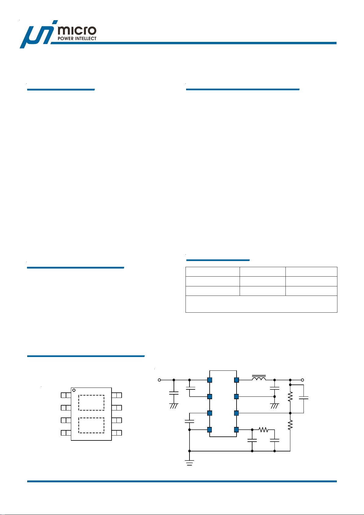
Ordering Information
rebmuNredrOepyTegakcaPkrameR
XX-8MSN6036PuL8-POSPSTEFSOMOKIN
XX-8MSU6036PuL8-POSPSTEFSOMQIBU
tnerruCnoitarepO:XXedoC
A5=50;A3=30:.g.e
Note: uPI products are compatible with the current IPC/
JEDEC J-STD-020 requirement. They are halogen-free,
RoHS compliant and 100% matte tin (Sn) plating that are
suitable for use in SnPb or Pb-free soldering processes.
1
VDD5
AGND
FB
Rev. F01, File Name: uP6306-DS-F0100
2
3
AGND
45
PSOP-8
8
LX
7
6
PGNDVIN
LX
VCC5
COMP/EN
Pin Configuration & Typical Application Circuit
R2
R1
V
OUT
Optional
V
IN
VIN
VDD5
VCC5
AGND
uP6306
LX
PGND
FB
COMP/EN
1uPI Semiconductor Corp., http://www.upi-semi.com
Page 2
.oNniPemaNniPnoitcnuFniP
n
uP6306
Functional Pin Descriptio
1NIV
25DDV
3DNGA
4BF
5NE/PMOC
65CCV
7XL
8DNGP
.tupnIylppuSrewoP ehtsrewopdnaegatlovtuptuoehtottnerrucseilppustahtegatlovtupnI
.srotalugerraenilV5lanretni
.revirDTEFSOMreppUrofylppuSsaiB morfroticapaccimarecFu7.4muminimatcennoC
.egatlovsaibehtssapybotnipNIVotnipsiht
.dnuorGlangiS .nipsihtotstnenopmoclangisllamsllafonruterehttcennoC
.egatloVkcabdeeF morfredividrotsiserA.reifilpmarorreehtottupnignitrevniehtsinipsihT
.egatlovnoitalugerehttesotdesusiDNGAottuptuoeht
.tuptuOreifilpmArorrE tupnignitrevni-nonehtdna)AE(reifilpmarorreehtfotuptuoehtsisihT
-egatlovehtetasnepmocotnipBFehthtiwnoitanibmocninipsihtesU.srotarapmocMWPehtfo
.retrevnocehtfopoolkcabdeeflortnoc
.ylppuSsaiB rewolehtroftnerrucgniylppus,rotalugerraenilV5lanretnifotuptuoehtsinipsihT
nipsihtmrofroticapaccimarecFu7.4muminimatcennoC.yrtiucriclanretnidnarevirdTEFSOM
.egatlovsaibehtssapybotnipDNGAot
.tuptuOsehctiwSlanretnI .rotcudnituptuoehtotnipsihttcennoC
.nruteRdnuorGrewoPniaM .nruterroticapactupnidnatuptuoehtottcennoC
.tuptuOsehctiwSlanretnI elpitlumhtiwBCPotderedlosllewebdluohsdapdesopxeehT
IdaPdesopxE
yllacirtceleebdluohsnipsihT.ecnamrofreplamrehtlamitporofenalpdnuorgotsaiv
.BCPnonipXLotdetcennoc
IIdaPdesopxE
.dnuorGlangiS .nipsihtotstnenopmoclangisllamsllafonruterehttcennoC
FB
AGND
COMP/EN
V
REF
(0.8V)
SS
Soft
Start
Error
Amplifier
0.8V
0.5V
VCC5
POR
Enable
Internal
Regulator
OCP
Comparator
PWM
Comparator
Oscillator
PWM
VDD5
300mV
Functional Block Diagram
Internal
Regulator
VDD5
Gate
Control
Logic
VCC5
VIN
LX
PGND
Rev. F01, File Name: uP6306-DS-F0100
2uPI Semiconductor Corp., http://www.upi-semi.com
Page 3
uP6306
Functional Description
The uP6306 is a high efficiency synchronous-rectified buck
converter with internal power switches. Fixed 300kHz PWM
operation allows possible smallest output ripple and
external component size. With high conversion efficiency
and small package, the uP6306 is ideally suitable for
applications where PCB area is especially concerned.
Designed with current mode control, the uP6306 features
fast transient response to step load change. The converter
supports PSM mode operation at light load condition, thus
yields very high efficiency over a wide range of load current.
With integrated high voltage MOSFET, the uP6306 is
capable of delivering 5A/3A output current over a wide input
range from 5V to 26V. The output voltage is adjustable
from 0.8V to 80% of VIN by a voltage divider. Other features
include internal soft-start, chip enable, under-voltage, overtemperature and over-current protections. The uP6306 is
available in a thermally enhanced PSOP-8 package.
Input Supply Voltage, V
IN
The uP6306 operates with single supply input at VIN pin.
The VIN pin supplies current for output voltages and provides
current for internal control circuit and gate drivers. The
supply voltage range is from 5V to 26V. The uP6306 draws
pulsed current from VIN pin with sharp edges each time
the upper switch turns on, resulting in voltage ripples and
spikes at supply input. A minimum 22uF ceramic capacitor
with shortest PCB trace is highly recommended for
bypassing the supply input.
The uP6306 integrates two 5V linear regulators. A linear
regulator regulates (VIN - VDD5) voltage at 5V for upper
gate driver. The other linear regulator regulates (VCC5 GND) voltage at 5V for internal control circuit and lower
gate driver. Both VDD5 and VCC5 need a minimum 4.7uF
capacitor for locally bypassing the output voltage of linear
regulators.
The VCC5 voltage is continuously monitored for power on
reset (POR) to insure its voltage is high enough for normal
operation. The POR threshold level is typically 4.2V at
VCC5 rising. For fixed VIN = 5V operation, connect VCC5
pin to VIN pin directly. Otherwise the dropout voltage of the
linear regulator will make VCC5 < 4.2V and below its POR
threshold voltage.
connected together to LX pin.
Bias Voltage
Internal linear regulators generate voltages for driving the
power MOSFET and biasing the internal control circuits.
The VDD5 voltage is regulated to -5V with respect to VIN
fro driving the PMOSFET. The gate of PMOSFET is driven
to VDD5 when turned on. A minimum 4.7uF ceramic
capacitor is required from VDD5 to VIN pin for locally
bypassing the VDD5 voltage.
The VCC5 is regulated to +5V with respective to AGND pin
for driving the NMOSFET and biasing the internal control
circuits. The gate of NMOSFET is driven to VCC5 when
turned on. A minimum 4.7uF ceramic capacitor is required
from VCC5 to AGND pin for locally bypassing the VCC5
voltage.
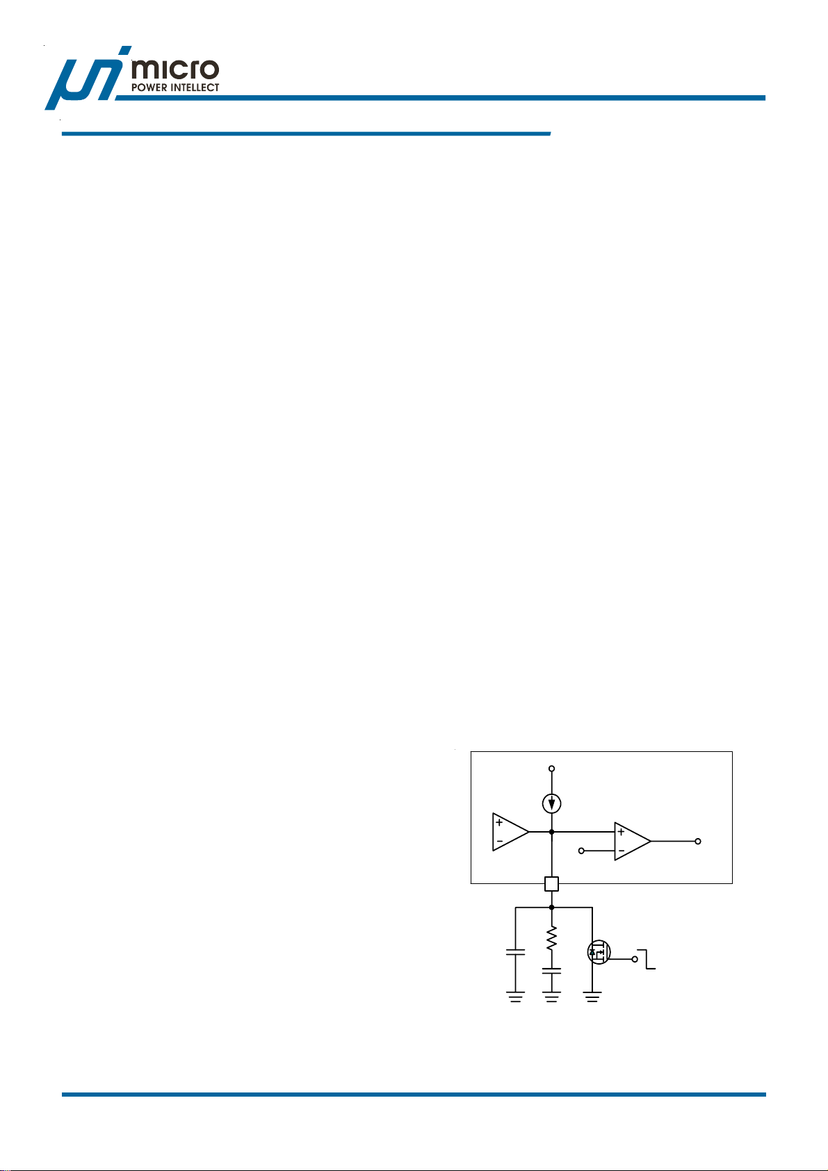
Chip Enable
The COMP/EN is a multifunctional pin: control loop
compensation and chip enable as shown in Figure 1. An
Enable Comparator monitors the COMP/EN pin for chip
enable. A signal level transistor is adequate to pull this pin
down to ground and shut down the uP6306. An 80uA current
source charges the external compensation network with
0.8V ceiling when this pin is released. If the voltage at
COMP/EN pin exceeds 0.5V, the uP6306 initiates its
softstart cycle.
The 80uA current source keeps charging the COMP/EN
pin to its ceiling until the feedback loop boosts the COMP/
EN pin higher than 0.8V according to the feedback signal.
The current source is cut off when V
is higher than
COMP
0.8V during normal operation.
Error
Amp.
0.8V
80uA
5
COMP/EN
0.5V
uP6306
Enable
Enable
Comp.
Power Switches
The uP6306 integrates internal power switches to form a
synchronous buck converter: 60mΩ(5A)/120mΩ(3A)
PMOSFET for upper switches 30mΩ(5A)/60mΩ(3A)
NMOSFET for lower switch. The source of PMOSFET is
connected to VIN pin, the source of NMOSFET is
connected to PGND pin. The drains of both MOSFETs are
Rev. F01, File Name: uP6306-DS-F0100
Disable
Enable
Figure 1. Chip Enable Function
3uPI Semiconductor Corp., http://www.upi-semi.com
Page 4
uP6306
Functional Description
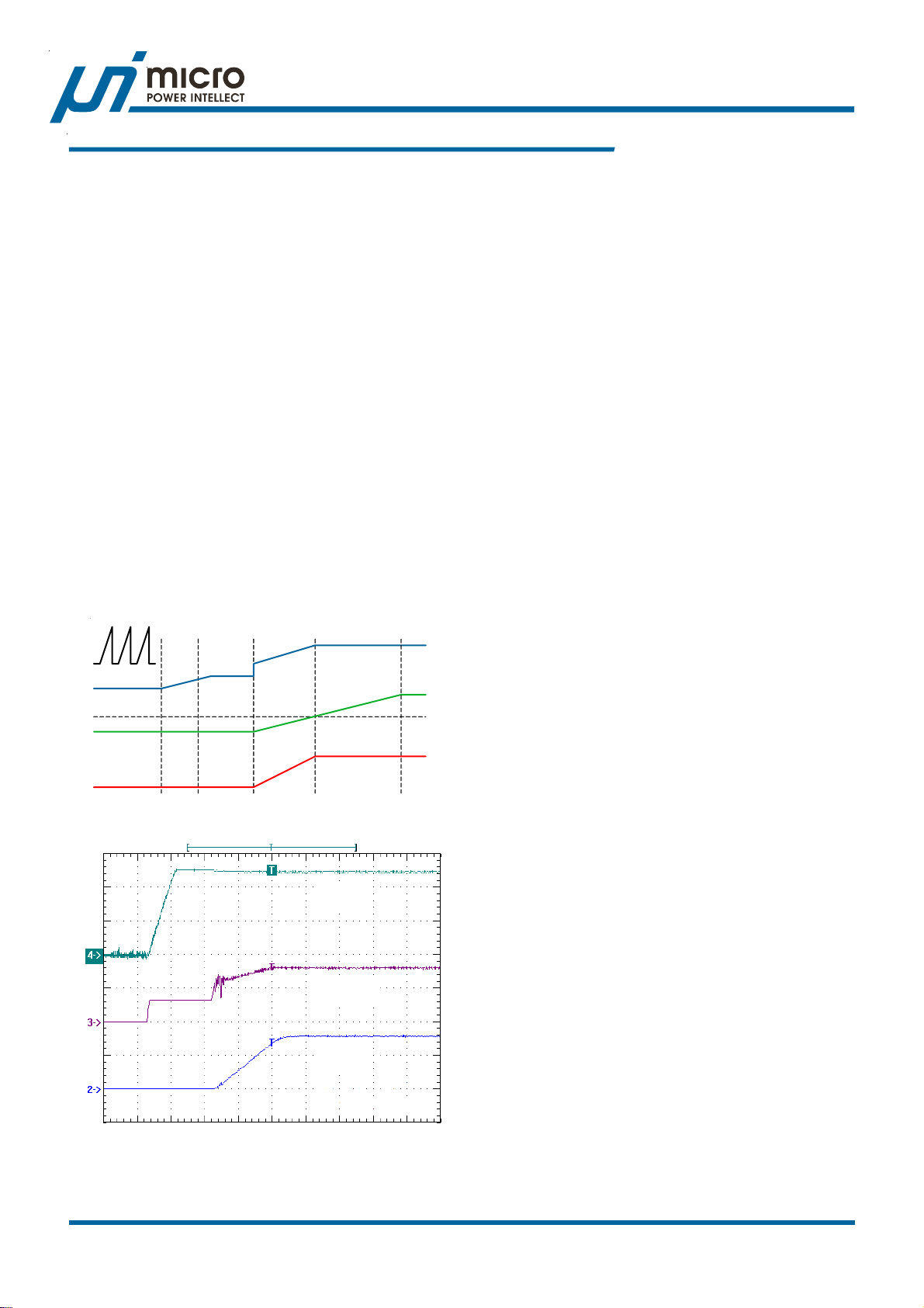
SoftStart
A built-in Soft Start is used to prevent surge current from
power supply input during turn on (referring to the Functional
Block Diagram). The error amplifier is a three-input device.
Reference voltage V
or the internal soft start voltage SS
REF
whichever is smaller dominates the behavior of the noninverting inputs of the error amplifier. SS internally ramps
up to 0.8V in 2ms after the softstart cycle is initiated. The
ramp is created digitally, so there will be 100 small discrete
steps. Accordingly, the output voltage will follow the SS
signal and ramp up smoothly to its target level.
The SS signal keeps ramping up after it exceeds the internal
0.8V reference voltage. However, the internal 0.8V reference
voltage takes over the behavior of error amplifier after SS >
V
. When the SS signal climb to its ceiling voltage (4V),
REF
the uP6306 claims the end of softstart cycle and enable
the under voltage protection of the output voltage.
Figure 2 shows a typical start up interval for uP6306 where
the COMP/EN pin has been released from a grounded
(system shutdown) state.
Ramp
COMP/EN
V
REF
T1 T2 T3 T4 T5
SS
V
OUT
The internal 80uA current source starts to charge the
compensation network after the COMP/EN pin is released
from grounded at T1. The COMP/EN exceeds 0.5V and
enables the uP6306 at T2. The COMP/EN continues
ramping up and stays at 0.8V before the SS starts ramping
up at T3. The uP6306 initializes itself such as current limit
level setting (see the relative section) during the time interval
between T2 and T3. The output voltage follows the internal
SS and ramps up to its final level during T3 and T4. At T4,
the reference voltage V
error amplifier as the internal SS crosses V
takes over the behavior of the
REF
. The internal
REF
SS keeps ramping up and stay at 4V at T5, where the
uP6306 asserts the end of softstart cycle.
PWM Operation
The uP6306 adopts slope-compensated, current mode
PWM control capable of achieving 80% duty cycle. During
normal operation, the uP6306 operates at PWM mode to
regulate output voltage by transferring the power to the
output voltage cycle by cycle at a constant 300kHz
frequency. The uP6306 turns on the upper switch at each
rising edge of the internal oscillator allowing the inductor
current to ramp up linearly. The switch remains on until
either the current-limit is tripped or the PWM comparator
turns off the switch for regulating output voltage. The upper
switch current is sensed, slope compensated and
compared with the error amplifier output COMP/EN to
determine the adequate duty cycle. The FB pin senses
output feedback voltage from an external resistive divider.
When the load current increases, it causes a slight
decrease in the feedback voltage relative to the 0.8V
reference, which in turn, causes the error amplifier output
voltage to increase until the average inductor current
matches the new load current.
Time 1ms/Div
Figure 2. Softstart Behavior.
Rev. F01, File Name: uP6306-DS-F0100
5VCC
(2V/Div)
COMP/EN
(1V/Div)
V
OUT
(2V/Div)
A Pseudo Diode Emulator monitors inductor current by
sensing voltage drop across the lower switch when it turns
on. The lower switch turns off to emulate the free wheel
diode used in traditional asynchronous buck converter and
allows the converter entering discontinuous conduction
mode when inductor current crosses zero. This reduces
conduction loss and increase power conversion efficiency
at light condition.
PSM Operation
A finite minimum on-time for both upper and lower switches
is implemented for normal operation. Consequently, the
converter will enter pulse-skipping mode (PSM) during
extreme light load condition or when modulation index (V
OUT
VIN) is extreme low. The equivalent switching frequency is
reduced. This could reduce switching loss and further
/
4uPI Semiconductor Corp., http://www.upi-semi.com
Page 5

increase power conversion efficiency. The lower switch turns
on with optimal deadtime and picks up the inductor current
after the upper switch turns off, allowing the inductor current
to ramp down linearly. The switch remains on until the next
rising edge of oscillator turns on the upper switch. The
uP6306 regulates the output voltage by controlling the ramp
up/down duty cycle of inductor current. The high frequency
switching ripple is easily smoothed by the output filter.
Current Limit Function
The uP6306 continuously monitors the inductor current for
current limit by sensing the voltage drop across the upper
switch when it turns on. When the inductor current is higher
than current limit threshold (7A(5A)/4.5A(3A) minimum),
the current limit function activates and forces the upper
switch turning off to limit inductor current cycle by cycle. If
the load continuously demands more current than what
uP6306 could provide, uP6306 can not regulate the output
voltage. Eventually under voltage protection will be triggered
and shuts down the uP6306 if V
is too low.
OUT
Undervoltage Protection
uP6306
Functional Description
Undervoltage Protection is triggered if the FB voltage is
lower than 0.4V and shuts down uP6306. The uP6306 can
only be reset by POR of VIN or toggling the COMP/EN pin.
Output Voltage Setting and Feedback Network
The output voltage can be set from V
to VIN by a voltage
REF
divider as:
2R1R
V ×
The internal V
+
=
V
REFOUT
1R
is 0.8V with 1.5% accuracy. In real
REF
applications, a 22pF feedforward ceramic capacitor is
recommended in parallel with R2 for better transient
response.
Rev. F01, File Name: uP6306-DS-F0100
5uPI Semiconductor Corp., http://www.upi-semi.com
Page 6

uP6306
A
g
n
bsolute Maximum Ratin
Supply Input Voltage, VIN (Note 1) -------------------------------------------------------------------------------------------------- -0.3V to +30V
LX to GND
DC ----------------------------------------------------------------------------------------------------------------------------- -0.7V to (VIN + 0.3V)
< 200ns ---------------------------------------------------------------------------------------------------------------------------- -5V to 40V
VDD to VIN ----------------------------------------------------------------------------------------------------------------------------- -6V to +0.3V
Other Pins -------------------------------------------------------------------------------------------------------------------------------------- -0.3V to +6V
Storage Temperature Range ------------------------------------------------------------------------------------------------------------ -65OC to +150OC
Junction Temperature ------------------------------------------------------------------------------------------------------------------------------------ 150OC
Lead Temperature (Soldering, 10 sec) ------------------------------------------------------------------------------------------------------------ 260OC
ESD Rating (Note 2)
HBM (Human Body Mode) --------------------------------------------------------------------------------------------------------------------- 2kV
MM (Machine Mode) ----------------------------------------------------------------------------------------------------------------------------- 200V
Thermal Informatio
Package Thermal Resistance (Note 3)
θJA PSOP-8 ------------------------------------------------------------------------------------------------------------------------------ 50°C/W
θJC PSOP-8 ------------------------------------------------------------------------------------------------------------------------------ 5°C/W
Power Dissipation, PD @ T
PSOP-8 ------------------------------------------------------------------------------------------------------------------------------------------------- 2W
= 25°C
A
Recommended Operation Conditions
Operating Junction Temperature Range (Note 4) ----------------------------------------------------------------------------- -40°C to +125°C
Operating Ambient Temperature Range -------------------------------------------------------------------------------------------- -40°C to +85°C
Supply Input Voltage, V
----------------------------------------------------------------------------------------------------------------- +5V to 26V
IN
Electrical Characteristics
(VIN = 12V, TA = 25OC, unless otherwise specified)
retemaraPlobmySsnoitidnoCtseTniMpyTxaMstinU
tupnIylppuS
egatloVylppuSV
tnerruCylppuStnecseiuQI
tnerruCnwodtuhSI
dlohserhTROPV
siseretsyHROPV
NI
V
Q_NI
DS_NI
HTR5CC
SYH5CC
TUO
V
5CC
I,V5=
gnisir--2.45.4V
ylppuSsaiB
5CCVV
V
NI
5DDV-V
5CC
5DD
A0=--9.0--Am
TUO
V,V0=NE/PMOC
V0=--0507Au
TUO
V6.0=NE/PMOC8.40.52.5V
V6.0=NE/PMOC7.40.53.5V
5--62V
--2.0--V
Rev. F01, File Name: uP6306-DS-F0100
6uPI Semiconductor Corp., http://www.upi-semi.com
Page 7

uP6306
Electrical Characteristics
retemaraPlobmySsnoitidnoCtseTniMpyTxaMstinU
rotallicsO
ycneuqerFgninnuReerFf
edutilpmApmaR ∆V
CSO
V
PMAR
V21=--21.1--V
NI
552003543zHk
elcyCytuDmumixaM 378738%
emiTnOmuminiMV
V6.1=--004--sn
TUO
egatloVecnerefeR
egatloVkcabdeeFlanimoNV
BF
97.008.018.0V
reifilpmArorrE
niaGCDpooLnepOOAngiseDybdeetnarauG0708--Bd
tcudorPhtdiwdnaB-niaGWBGngiseDybdeetnarauG--03--zHM
ecnatcudnocsnarT --002--Su
tnerruCecruoStuptuOV
tnerruCkniStuptuOV
V<
BF
BF
FER
V>
FER
4223--Au
4223--Au
dlohserhTelbasiDpihCgnillafNE/PMOC--5.0--V
tnerruChgiH-lluPNE/PMOCV0=NE/PMOC--25Au
sehctiwSrewoP
A5=tnerruCnoitarepO--06--mΩ
ecnatsiseRnOhctiwSreppUR
)NO(SD
A3=tnerruCnoitarepO--021--mΩ
ecnatsiseRnOhctiwSrewoLR
)NO(SD
A3=tnerruCnoitarepO--06--mΩ
A5=tnerruCnoitarepO7--01A
timiLtnerruChctiwSrewoL
A3=tnerruCnoitarepO5.4--5.7A
noitcetorP
A5=tnerruCnoitarepO--03--mΩ
noitcetorPegatloVrednUtuptuOV
V
PVU_BF
noitcetorPerutarepmeTrevO --051--
gnillaf--4.0--V
BF
O
Note 1. Stresses listed as the above “Absolute Maximum Ratings” may cause permanent damage to the device.
These are for stress ratings. Functional operation of the device at these or any other conditions beyond those
indicated in the operational sections of the specifications is not implied. Exposure to absolute maximum
rating conditions for extended periods may remain possibility to affect device reliability.
Note 2. Devices are ESD sensitive. Handling precaution recommended.
Note 3. θ
is measured in the natural convection at T
JA
= 25°C on a low effective thermal conductivity test board of
A
JEDEC 51-3 thermal measurement standard.
Note 4. The device is not guaranteed to function outside its operating conditions.
C
Rev. F01, File Name: uP6306-DS-F0100
7uPI Semiconductor Corp., http://www.upi-semi.com
Page 8

uP6306
Typical Operation Characteristics
Efficiency vs. Output Current
100
90
80
70
60
Efficiency (%)
50
40
30
1 10 100 1000 10000
Output Current (mA)
Switching Frequency vs. Input Voltage
320
315
310
305
VCC5 Voltage Line Regulation
6
5
4
3
2
VCC5 Voltage (V)
1
0
0 5 10 15 20 25 30
Input Voltage (V)
Power On Waveforms
V
IN
(2V/Div)
VCC5
(2V/Div)
300
295
290
Switching Freqeuncy (kHz)
285
280
5 1015202530
Input Voltage (V)
Power Off Wavefroms
V
(2V/Div)
5VCC
(2V/Div)
COMP/EN
(1V/Div)
V
(2V/Div)
OUT
V
OUT
(2V/Div)
COMP/EN
(1V/Div)
Time (1ms/Div)
VIN = 5V, V
= 3.3V, I
OUT
OUT
= 1A.
Turn On Waveforms
IN
VCC5
(2V/Div)
COMP/EN
(2V/Div)
V
OUT
(2V/Div)
Time (1ms/Div)
VIN = 5V, V
= 3.3V, I
OUT
Rev. F01, File Name: uP6306-DS-F0100
OUT
= 1A.
Time (1ms/Div)
VIN = 5V, V
= 3.3V, I
OUT
OUT
= 1A.
8uPI Semiconductor Corp., http://www.upi-semi.com
Page 9

uP6306
Typical Operation Characteristics
Turn Off Waveforms
V
OUT
(1V/Div)
VCC5
(2V/Div)
COMP/EN
(1V/Div)
Time (250us/Div)
VIN = 5V, V
= 3.3V, I
OUT
Load Transient Response
V
OUT
(50mV/Div)
OUT
= 1A.
Steady State Operation
V
OUT
(20mV/Div)
LX
(5V/Div)
I
LX
(2A/Div)
Time (2.5us/Div)
VIN = 5V, V
= 3.3V, I
OUT
OUT
= 2A.
Load Transient Response
V
OUT
(50mV/Div)
LX
(10V/Div)
I
LX
(5A/Div)
Time (5us/Div)
VIN = 20V, V
= 3.3V, I
OUT
OUT
Over Current Protection
V
OUT
(2V/Div)
= 0 to 5A.
LX
(10V/Div)
I
(10A/Div)
LX
(10V/Div)
I
LX
(5A/Div)
Time (5us/Div)
VIN = 20V, V
LX
= 3.3V, I
OUT
= 5 to 0A.
OUT
Time (5us/Div)
VIN = 12V, V
OUT
Rev. F01, File Name: uP6306-DS-F0100
= 3.3V.
9uPI Semiconductor Corp., http://www.upi-semi.com
Page 10

A
pplication Information
This page is intentionally left blank and will be updated when silicon data are available.
uP6306
10uPI Semiconductor Corp., http://www.upi-semi.com
Rev. F01, File Name: uP6306-DS-F0100
Page 11

uP6306
n
Package Informatio
0.70 REF
7.00 REF
5.50 REF
0.30 MIN
3.00 REF
1.27 REF
2.20 REF
1.50 REF
5. 80 - 6. 20
4.00 REF
3. 80 - 4. 00
1.27 BSC
4.80 - 5.00
3.00 BSC
2.20 BSC
0.32 - 0.52
Recommended Solder Pad Layout
1.45 - 1.60
0.20 BSC
0.40 - 0.90
0.18 - 0.25
1.75 MAX
0.05 - 0.25
3.81 BSC
Note
1.Package Outline Unit Description:
BSC: Basic. Represents theoretical exact dimension or dimension target
MIN: Minimum dimension specified.
MAX: Maximum dimension specified.
REF: Reference. Represents dimension for reference use only. This value is not a device specification.
TYP. Typical. Provided as a general value. This value is not a device specification.
2.Dimensions in Millimeters.
3.Drawing not to scale.
4.These dimensions do not include mold flash or protrusions. Mold flash or protrusions shell not exceed 0.15mm.
Rev. F01, File Name: uP6306-DS-F0100
11uPI Semiconductor Corp., http://www.upi-semi.com
Page 12

 Loading...