

Page 1
DATEL, Inc., Mansfield, MA 02048 (USA) · Tel: (508)339-3000, (800)233-2765 Fax: (508)339-6356 · Email: sales@datel.com · Internet: www.datel.com
Single Output
UNS Series
Features
Figure 1. Simplified Schematic
+V
IN
+V
OUT
PWM
CONTROLLER
REFERENCE &
ERROR AMP
ON/OFF
CONTROL
TRIM
+V
IN
–V
IN
–V
IN
+V
OUT
OUTPUT
RETURN
OUTPUT
RETURN
Non-Isolated, 3.3V and 5V
3 Amp, DC/DC Converters
Low cost, high efficiency, wide input voltage range and low output noise define
DATEL’s new UNS Series of non-isolated, step-down, switching DC/DC converters.
The 3.3V- and 5V-output devices are, respectively, 90% and 92% efficient. All
models are fully line and load regulated and maintain specified accuracy over the
impressively wide input voltage ranges of 4.75 to 13.6 Volts for 3.3V outputs and 6
to 16.5 Volts for 5V outputs. Output ripple and noise are typically 50mVp-p.
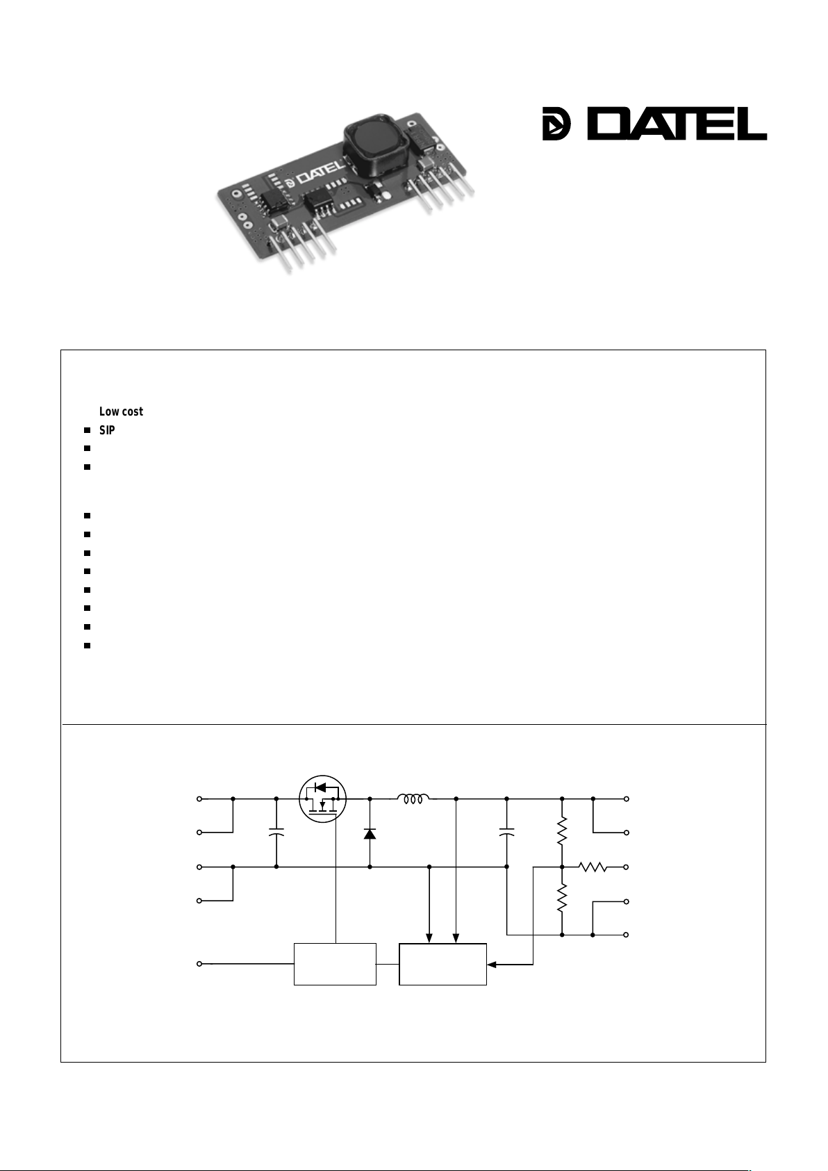
UNS devices are fabricated using proven SMT-on-pcb construction techniques.
The 3.3V and 5V devices are both available in either lightweight SIP (2" x 0.4" x
0.8") or DIP (2" x 0.8" x 0.4", 600 mil spacing between rows) package configurations. The DIP option is designated by a "D" suffix added to the part number. All
models are conformally coated for protection against moisture and dust.
The high efficiency of the UNS Series’ fixed-frequency (190kHz) switching
design eliminates the need for thermally conductive potting compound. Devices are
specified for full-power operation up to ambient temperatures of +50°C. With
derating, they operate up to +70°C. Calculated MTBF (MIL-HDBK-217F) is more
than 1.6 million hours.
These simple-to-use power converters have no minimum load requirements.
They draw 1mA when unloaded and a mere 100µA in the standby mode (On/Off
Control turned off). 3.3V models have an output voltage adjustment range of 2.7 to
3.3 Volts. 5V models are adjustable down to 3.0V.
INNOVATION and EX C ELL E N C E
®
®
■
n
n
n
n
n
n
n
n
n
n
n
Low cost
SIP or DIP packaging
3.3V (10W) or 5V (15W) outputs
Wide range inputs:
4.75-13.6V for 3.3V models
6-16.5V for 5V models
High efficiencies, typically 90-92%
Low output noise, 50mVp-p
Remote on/off control
100µA "standby" input current
Output current limiting
EMC compliant
Highly reliable, 100% SMT construction
Conformally coated for harsh
environments
Page 2
UNS Series
NON-ISOLATED, 10 and 15W, SINGLE OUTPUT DC/DC CONVERTERS
2
Case B1 (SIP)
PART NUMBER STRUCTURE
MECHANICAL SPECIFICATIONS
0.900
(22.86)
1.97
(50.00)
0.400
(10.16)
0.81
(20.50)
0.03
(0.8)
0.1
(2.5
)
0.28
(7.0)
0.07
(1.85)
12345 678910
4 EQ. SP. @
0.100 (2.54)
0.400
(10.16)
4 EQ. SP. @
0.100 (2.54)
0.13
(3.41)
0.30
(7.62)
0.025
(0.64)
Case B2 (DIP)
0.900
(22.86)
1.97
(50.00)
0.400
(10.16)
0.81
(20.50)
0.03
(0.8)
0.14
(3.5)
0.28
(7.0)
12345 678910
4 EQ. SP. @
0.100 (2.54)
0.400
(10.16)
4 EQ. SP. @
0.100 (2.54)
0.13
(3.41)
0.40
(10.16)
0.025
(0.64)
0.60
(15.24)
0.10
(2.63)
**
* NO CONNECTION. FOR MECHANICAL STABILITY ONLY.
STANDOFF
Input Voltage Range:
D5 = 4.75-13.6 Volts (7.5V nominal)
D12 = 6-16.5 Volts (12V nominal)
Nominal Output Voltage:
3.3 or 5 Volts Maximum Output Current
in Amps
Non-Isolated
SIP packaging
Output Configuration:
U = Unipolar
Add "D" suffix for optional
DIP package configuration
3.3U NS 3 D5 D-
/
-
I/O Connections
Pin
6
7
8
9
10
Function P18
Trim
Output Rtn.
Output Rtn.
+Output
+Output
Function P18
+Input
+Input
–Input
–Input
On/Off Control
Pin
1
2
3
4
5
TEMPERATURE DERATING
Output Power (Watts)
Ambient Temperature (°C)
20
18
16
14
12
10
8
6
4
2
0
–10 0 10 20 30 40 50 60 70 80 90 10
0
UNS-3.3/3-D5
UNS-5/3-D12
Note: Derating curves apply to both SIP and DIP package configurations
Performance Specifications and Ordering Guide
➀
IOUT
(Amps)
R/N (mVp-p)
Â
Load
VOUT
(Volts)
Package
(Case,
Pinout)
Efficiency
Regulation (Max.)
Ã
Line
VIN Nom.
(Volts)
Range
(Volts)
Model
Á
IIN ➄
(mA)
Max.
Typ.
Typ.
Min.
Output Input
UNS-3.3/3-D5 3.3 3 50 100 ±1.0% ±3.0% 7.5 4.75-13.6 1/1400 -- 90% B1, P18
UNS-3.3/3-D5D 3.3 3 50 100 ±1.0% ±3.0% 7.5 4.75-13.6 1/1400 -- 90% B2, P18
UNS-5/3-D12 5 3 50 100 ±1.0% ±3.0% 12 6-16.5 1/1330 -- 92% B1, P18
UNS-5/3-D12D 5 3 50 100 ±1.0% ±3.0% 12 6-16.5 1/1330 -- 92% B2, P18
➀
Typical at TA = +25°C under nominal line voltage and full-load conditions, unless otherwise noted.
➁
"D" suffix indicates DIP package.
➂
Ripple/Noise (R/N) measured over a 20MHz bandwidth with a 100µF external input capacitor and a
220µF external output capacitor. Additional ouput capacitors will lower R/N. See T echnical Notes.
➃
Listed output regulation specifications describe the total change in output voltage as the input (line)
voltage or output (load) current is varied over its full specified range. Typically , line regulation is
better than ±0.5% and load regulation is better than ±1.0%. Load regulation applies for 0 to 100% load conditions.
➄
Nominal line voltage, no-load/full-load conditions.
Page 3

NON-ISOLATED, 10 and 15W, SINGLE OUTPUT DC/DC CONVERTERS
UNS Series
3
TECHNICAL NOTES
Input Voltage:
"D5" Models 15 Volts
"D12" Models 18 Volts
Input Reverse-Polarity Protection None. See Technical Notes.
Output Overvoltage Protection None
Output Current Current limited. Devices can
withstand an output short circuit
for brief durations only.
Storage Temperature –25 to +85°C
Lead Temperature (soldering, 10 sec.) +300°C
These are stress ratings. Exposure of devices to any of these conditions may adversely
affect long-term reliability . Proper operation under conditions other than those listed in the
Performance/Functional Specifications T able is not implied.
Absolute Maximum Ratings
Input and Output Capacitors
Though UNS Series, non-isolated, DC/DC converters have on-board input
and output capacitors (C
IN = 6.8µF, COUT = 6.8µF), the majority of applica-
tions will require the installation of additional external I/O capacitance.
The total input capacitance functions as a true energy-storage element, and
its optimal value will vary as a function of line voltage. The selected external
input capacitor should have both low ESR and low ESL because, as the
power converter’s input FET switch cycles on and off, the input capacitance
must have the ability to instantaneously supply pulses of relatively high
current.
Rather than install a large, expensive, on-board capacitor that addresses all
possible input-voltage and output-load conditions, DATEL has chosen to
leave out the bulk of the input capacitance so that users may select a costeffective component appropriate to their own application. We use a low-ESR
100µF external input capacitor during production testing and have found
330µF to be a conservative value that works well in the majority of applications.
In addition to their on-board output capacitor, UNS Series devices require the
installation of additional output capacitors to achieve rated ripple/noise
specifications. External output capacitors should be low-ESR tantalum or
electrolytic types, and they should be located as close to the converters as
possible. A minimum of 220µF is required to achieve rated ripple/noise
specs. Increased capacitance will lower output noise. There are no limitations
on output capacitance; however, we have found minimal noise improvements
beyond 4700µF .
Typical @ TA = +25°C under nominal line voltage and full-load conditions, unless noted.
➀
➀
UNS Series devices require external input/output capacitors to achieve rated performance.
Listed specifications assume C
IN = 100µF and COUT = 220µF .
➁
See T echnical Notes.
➂
Output Ripple/Noise can be reduced with external capacitors. See T echnical Notes.
➃
UNS Series converters have no minimum-load requirements.
➄
Current limiting initiates at approximately 5% above rated load.
➅
DIP models have a standoff which makes their total above-board height 0.44 inches.
Input
Input Voltage Range:
"D5" and "D5D" Models 4.75-13.6 Volts (7.5V nominal)
"D12" and "D12D" Models 6-16.5 Volts (12V nominal)
Input Current See Ordering Guide
Input Filter Type Capacitive
Overvoltage Protection None
Reverse-Polarity Protection None
On/Off Control (Pin 5)
➁
TTL high (or open) = on, low = off
Output
VOUT Accuracy ±5%, maximum
Temperature Coefficient ±0.01% per °C
Ripple/Noise (20MHz bandwidth) ➂See Ordering Guide
Line/Load Regulation
➃
See Ordering Guide
Efficiency See Ordering Guide
Current Limiting
➄
Auto-recovery
Dynamic Characteristics
Transient Response (50% load step) 200µsec max. to ±2% of final value
Switching Frequency 190kHz
Environmental
Operating Temperature:
Without Derating –10 to +50°C
With Derating to +70°C (See Derating Curve)
Storage Temperature –25 to +85°C
Physical
Dimensions: SIP Models 2 x 0.41 x 0.8" (50 x 10.3 x 21mm)
DIP Models
➅
2 x 0.8 x 0.44" (50 x 21 x 11.3mm)
Shielding None
Case Connection None
Pin Material Gold-plated phosphor bronze
Weight 0.35 ounces (10 grams)
Page 4

UNS Series
NON-ISOLATED, 10 and 15W, SINGLE OUTPUT DC/DC CONVERTERS
Output Trimming
5V devices can be trimmed down to 3.0V, and 3.3V devices can be trimmed
down to 2.7V using a single external trimpot or fixed resistor. The trimpot
should be connected between +V
OUT (pins 9 and 10) and Trim (pin 6) as
shown in the figure below. The trimpot can be used to determine the value of
a single fixed resistor which can then be connected between pins 9 and 10
and 6. Fixed resistors should be metal-film types with relatively low absolute
TCR’s to ensure stability .
In order to maximize their efficiency , UNS devices employ high-value
resistors in their voltage feedback loop. Consequently, the external trimpots
must also be high-resistance devices (1-2 megohms). If the trimpots are
accidentally turned to their 0
W
stops, it will not damage the converters;
however, the output voltage will be pulled down to an unstable level. Use care
not to trim the output voltage below the levels indicated in the accompanying
table.
100
98
96
94
92
90
88
86
84
Efficiency (%)
3.3V Output Current (Amps)
VIN = 13.6V
VIN = 7.5V
V
IN
= 4.75V
0 0.5 1.0 1.5 2.0 2.5 3.
0
100
98
96
94
92
90
88
86
84
Efficiency (%)
5V Output Current (Amps)
VIN = 16.5V
VIN = 12V
V
IN
= 6V
0 0.5 1.0 1.5 2.0 2.5 3.0
OUTPUT
RETURN
+OUTPUT
R
LOA
D
TRIM
ERROR
AMP
1.195V
R1
R3
R2
R
TRIM
6
7, 8
9, 10
Figure 2. Output V oltage Trimming
Product UNS-3.3/3 UNS-5/3
Output Voltage
Adjustment Range
2.7 to 3.3V 3.0 to 5.0V
R1 68.68kW 124.7
k
W
R2 38kW 39
k
W
R3 10kW 10kW
RTRIM ³160kW³100kW
Table 1. Output Voltage Trim Values
Efficiency vs. Output Current and Input Voltage (Model UNS-5/3)
TYPICAL PERFORMANCE CURVES
Efficiency vs. Output Current and Input Voltage (Model UNS-3.3/3)
The On/Off Control Pin
For normal operation, pin 5 should be left open. This pin has an internal
250k
W
pull-up resistor to +5V (or to +VIN if +VIN < 5V). For dynamic control of
the converters’ on/off functionality, a TTL logic high (+2.4V minimum, +5V
maximum or +VIN maximum if +VIN < 5V, 100µA max.) applied to pin 5
enables the converter, and a quasi-TTL logic low (0 to +0.5V, 100µA max.)
disables the converter. Control voltages should be referenced to pins 3 and 4
(–Input). For best results, use a mechanical relay or open-collector logic.
When the converter is turned off, its input "standby" current will be approximately 100µA. Applying a voltage that is greater than V
IN to the On/Off
Control pin, or applying any voltage to this pin when no input power is
applied to the converter, may cause permanent damage to the converter.
DS-0406 9/98
DATEL makes no representation that the use of its products in the circuits described herein, or the use of other technical information contained herein, will not infringe upon existing or future patent rights. The descriptions contained herein
do not imply the granting of licenses to make, use, or sell equipment constructed in accordance therewith. Specifications are subject to change without notice. The DATEL logo is a registered DATEL, Inc. trademark.
DATEL (UK) LTD. Tadley, England Tel: (01256)-880444
DATEL S.A.R.L. Montigny Le Bretonneux, France Tel: 01-34-60-01-01
DATEL GmbH München, Germany Tel: 89-544334-0
DATEL KK Tokyo, Japan Tel: 3-3779-1031, Osaka Tel: 6-354-2025
DATEL, Inc. 11 Cabot Boulevard, Mansfield, MA 02048-1151
Tel: (508) 339-3000 (800) 233-2765 Fax: (508) 339-6356
Internet: www.datel.com Email: sales@datel.com
Data Sheet Fax Back:(508) 261-2857
INNOVATION and EX C ELL E N C
E
®
®
ISO-9001 REGISTERED
Page 5

INNOVATIO N and EX C ELL E N C E
® ®
DATEL, Inc., Mansfield, MA, USA • Tel: (508)339-3000, (800)233-2765 • Fax: (508)339-6356 • Email: sales@datel.com
Data sheet fax back: (508)261-2857 • Visit us on the internet: www.datel.com
3
12 (6-16.5) 2 x 0.4 x 0.8 ➃ B1, P18 ±1.0% ±3.0% 50 92% ➅ UNS-5/3-D12 UNS, 10/15W
12 (6-16.5) 2 x 0.8 x 0.4 ➄ B2, P18 ±1.0% ±3.0% 50 92% ➅ UNS-5/3-D12D UNS, 10/15W
5 ➆ 12 (10.4-13.6) 2 x 1 x 0.48 C13, P21 ±0.25% ±0.5% 60 87% UNR-5/5-D12 UNR, 25W
Listed specifications are typical at TA = +25°C under nominal line voltage and full-load conditions, unless noted.
➀ See individual product data sheets for mechanical specifications and pinouts.
➁ Ripple/Noise is specified over a 20MHz bandwidth.
➂ Listed specifications for these products are preliminary.
➃ 10-pin SIP package.
➄ 10-pin DIP package.
➅ Listed specification is a typical.
➆ Output voltage is user adjustable from 3.3 to 6V.
➇ Output voltage is user adjustable from 1.4 to 3.6V.
➈ Industry-standard, 11-pin SIP package.
NON-ISOLATED DC/DC CONVERTER SELECTION GUIDE
NON-ISOLATED DC/DC CONVERTER SELECTION GUIDE
Output Input Voltage, Ripple/
Current Nominal (Range) Dimensions Case, Line Load Noise ➁ Efficiency DATEL Data Sheet @
(Amps, Max.) (Volts) (Inches) Pinout (Max.) (Max.) (mVp-p) (Min.) Model Number www.datel.com
Package ➀ Regulation
2.5V
SINGLE OUTPUT, NON-ISOLATED
2.5V
SINGLE OUTPUT, NON-ISOLATED
Rev. C 6/99
5V
SINGLE OUTPUT, NON-ISOLATED
5V
SINGLE OUTPUT, NON-ISOLATED
2 5 (4.75-5.5) 1 x 1 x 0.45 C7A, P9 ±0.25% ±0.5% 30 83% UNR-2.5/2-D5 UNR, 5W
8
5 (4.75-5.5) 2 x 1 x 0.39 C5A, P9 ±0.1% ±0.5% 40 86% UNR-2.5/8-D5 UNR, 20/25W
12 (10.4-13.6) 2 x 1 x 0.48 C5C, P9 ±0.1% ±0.6% 40 85% UNR-2.5/8-D12 UNR, 20/25W
10
5 (4.75-5.5) 2 x 1 x 0.39 C5A, P9 ±0.1% ±0.5% 40 85% UNR-2.5/10-D5 UNR, 20/25W
12 (10.4-13.6) 2 x 1 x 0.48 C5C, P9 ±0.1% ±0.6% 40 83% UNR-2.5/10-D12 UNR, 20/25W
12 5 (4.75-5.5) 2 x 1 x 0.44 C5B, P9 ±0.1% ±0.5% 40 84% UNR-2.5/12-D5 UNR, 30W
20 5 (4.5-5.5) 2 x 2 x 0.49 C21, P26 ±0.1% ±1.0% 60 85% UNR-2.5/20-D5 ➂ Contact DATEL
5 (4.75-5.5) 1 x 1 x 0.45 C7A, P9 ±0.4% ±0.5% 30 86% UNR-3.3/3-D5 UNR, 10W
3
7.5 (4.75-13.6) 2 x 0.4 x 0.8 ➃ B1, P18 ±1.0% ±3.0% 50 90% ➅ UNS-3.3/3-D5 UNS, 10/15W
7.5 (4.75-13.6) 2 x 0.8 x 0.4 ➄ B2, P18 ±1.0% ±3.0% 50 90% ➅ UNS-3.3/3-D5D UNS, 10/15W
12 (10.4-13.6) 1 x 1 x 0.45 C7A, P9 ±0.25% ±0.5% 100 87% UNR-3.3/3-D12 UNR, 10W
5 (4.75-5.5) 2 x 1 x 0.39 C5A, P9 ±0.1% ±0.5% 40 88% UNR-3.3/8-D5 UNR, 26/33W
5 (4.75-5.5) 2 x 1 x 0.39 C16A, P23 ±0.1% ±0.5% 40 88% UNR-3.3/8-D5T ➂ ➇ Contact DATEL
8 5 (4.75-5.5) 2 x 0.4 x 0.53 ➈ B3, P27 ±0.1% ±0.5% 40 88% USN-3.3/8-D5 ➂ Contact DATEL
12 (10.4-13.6) 2 x 1 x 0.48 C5C, P9 ±0.1% ±0.6% 60 86% UNR-3.3/8-D12 UNR, 26/33W
12 (10.4-13.6) 2 x 1 x 0.48 C16C, P23 ±0.1% ±0.6% 60 86% UNR-3.3/8-D12T ➂ ➇ Contact DATEL
5 (4.75-5.5) 2 x 1 x 0.39 C5A, P9 ±0.1% ±0.5% 40 86% UNR-3.3/10-D5 UNR, 26/33W
5 (4.75-5.5) 2 x 1 x 0.39 C16A, P23 ±0.1% ±0.5% 40 86% UNR-3.3/10-D5T ➂ ➇ Contact DATEL
10 5 (4.75-5.5) 2 x 0.4 x 0.53 ➈ B3, P27 ±0.1% ±0.5% 40 86% USN-3.3/10-D5 ➂ Contact DATEL
12 (10.4-13.6) 2 x 1 x 0.48 C5C, P9 ±0.1% ±0.6% 60 85% UNR-3.3/10-D12 UNR, 26/33W
12 (10.4-13.6) 2 x 1 x 0.48 C16C, P23 ±0.1% ±0.6% 60 85% UNR-3.3/10-D12T ➂ ➇ Contact DATEL
12 5 (4.75-5.5) 2 x 1 x 0.44 C5B, P9 ±0.1% ±0.5% 40 87% UNR-3.3/12-D5 UNR, 40W
20 5 (4.5-5.5) 2 x 2 x 0.49 C21, P26 ±0.1% ±1.0% 50 87% UNR-3.3/20-D5 ➂ Contact DATEL
3.3V
SINGLE OUTPUT, NON-ISOLATED
3.3V
SINGLE OUTPUT, NON-ISOLATED
 Loading...