

Page 1

INTEGRATED CIRCUITS
DATA SH EET
TZA3034T; TZA3034U
SDH/SONET STM1/OC3
postamplifiers
Objective specification
File under Integrated Circuits, IC19
1998 Jul 07
Page 2
Philips Semiconductors Objective specification
SDH/SONET STM1/OC3 postamplifiers TZA3034T; TZA3034U
FEATURES
• Pin compatible with the NE/SA5224 and NE/SA5225 but
with extended power supply range and less external
component count
• Wideband operation from 1.0 kHz to 150 MHz typical
APPLICATIONS
• Digital fibre optic receiver in short, medium and long
haul optical telecommunications transmission systems
or in high speed data networks
• Wideband RF gain block.
• Applicable in 155 Mbits/s SDH/SONET receivers
• Single supply voltage from 3.0 to 5.5 V
• PECL (Positive Emitter Coupled Logic) compatible data
outputs
• Programmable input signal level-detection which can be
adjusted using a single external resistor
• On-chip DC offset compensation without external
capacitor
• Fully differential for excellent PSRR.
GENERAL DESCRIPTION
The TZA3034 is a high gain limiting amplifier that is
designed to process signals from fibre optic preamplifiers
like the TZA3033. It is pin compatible with the NE/SA5224
and NE/SA5225 but with extended power supply range,
and needs less external components. Capable of
operating at 155 Mbits/s, the chip has input signal level
detection with a user-programmable threshold. The data
and level-detection status outputs are differential outputs
for optimum noise margin and ease of use.
ORDERING INFORMATION
TYPE
NUMBER
NAME DESCRIPTION VERSION
PACKAGE
TZA3034T SO16 plastic small outline package; 16 leads; body width 3.9 mm SOT109-1
TZA3034U naked die die in waffle pack carriers; die dimensions 1.58 × 1.58 mm −
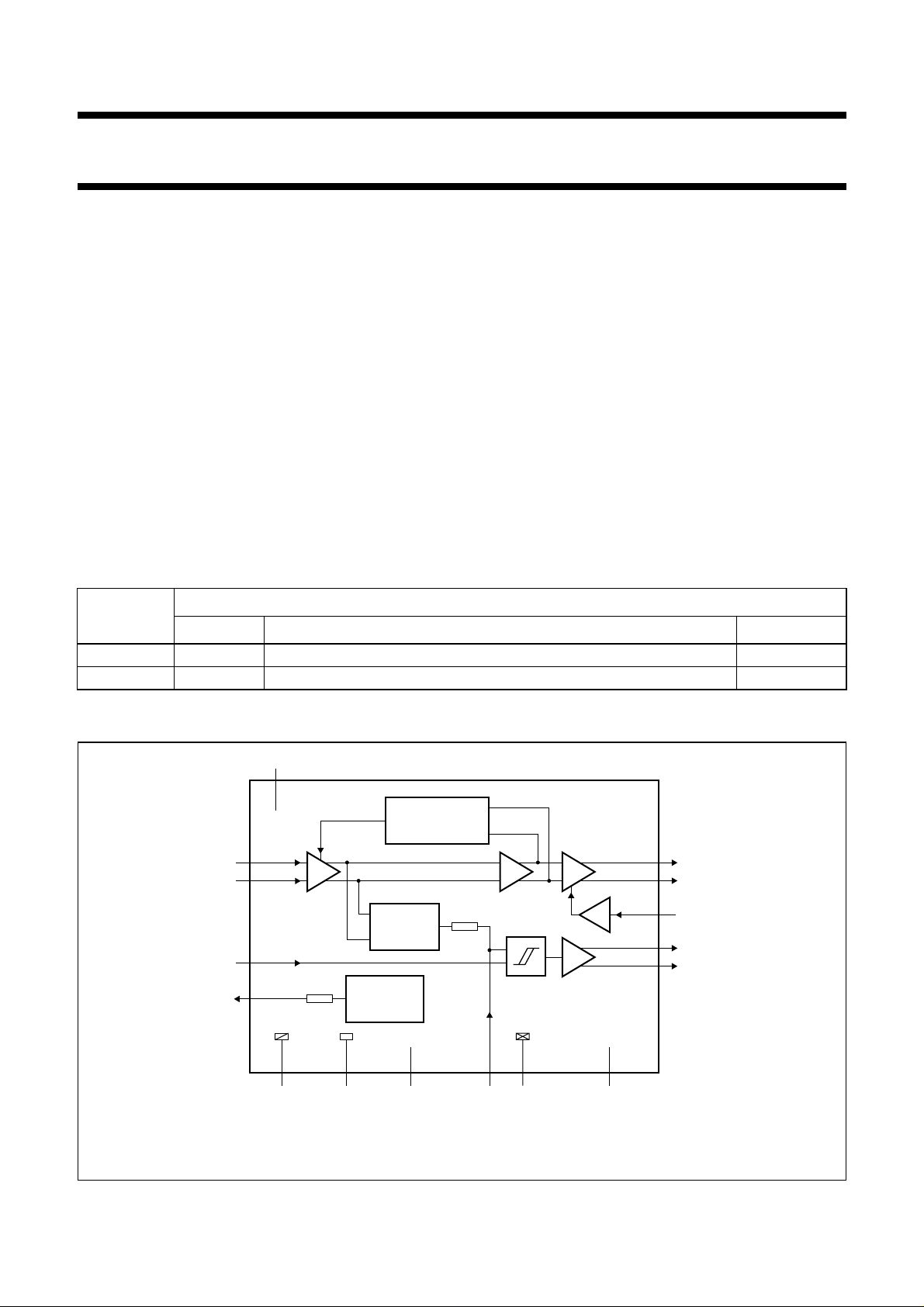
BLOCK DIAGRAM
ref
TEST
2
(2, 10, 15, 21, 26)
4 (7)
5 (8)
16 (30)
15 (29)
AGND V
A1 A2 A3
1 kΩ
(3, 4, 6, 9)
3
BAND GAP
REFERENCE
(1, 14)
1
SUB
DC-OFFSET
COMPENSATION
RECTIFIER
CCA
handbook, full pagewidth
DIN
DINQ
RSET
V
The numbers in brackets refer to the pad numbers of the naked die version.
Fig.1 Block diagram.
(11, 12)
6
25 kΩ
(19, 20, 22, 25)11(27, 28)
(13)
7
CF
DGND V
TZA3034
A4
CCD
(24) 13
(23) 12
(16) 8
(18) 10
(17) 9
14
DOUT
DOUTQ
JAM
ST
STQ
MGR281
1998 Jul 07 2
Page 3

Philips Semiconductors Objective specification
SDH/SONET STM1/OC3 postamplifiers TZA3034T; TZA3034U
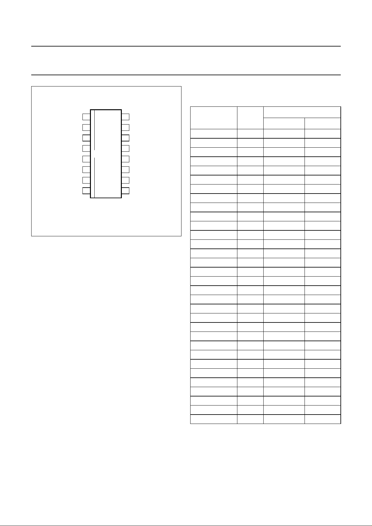
PINNING
SYMBOL PIN TYPE DESCRIPTION
SUB 1 substrate substrate pin; must be at the same potential as AGND (pin 3)
TEST 2 test pin for test purpose only; to be left open in the application
AGND 3 ground analog ground; must be at the same potential as DGND (pin 11)
DIN 4 analog input differential input; DC bias level is set internally at approximately 2.55 V;
complimentary to DINQ (pin 5)
DINQ 5 analog input differential input; DC bias level is set internally at approximately 2.55 V;
complimentary to DIN (pin 4)
V
CCA
CF 7 analog input filter capacitor for input signal level detector; capacitor should be connected
JAM 8 PECL input PECL-compatible input; controls the output buffers DOUT and DOUTQ
STQ 9 PECL output PECL-compatible status output of the input signal level detector; when the input
ST 10 PECL output PECL-compatible status output of the input signal level detector; when the input
DGND 11 ground digital ground; must be at the same potential as AGND (pin 3)
DOUTQ 12 PECL output PECL-compatible differential output; when JAM is HIGH, this pin will be forced
DOUT 13 PECL output PECL-compatible differential output; when JAM is HIGH, this pin will be forced
V
CCD
V
ref
RSET 16 analog input input signal level detector programming; nominal DC voltage is V
6 supply analog supply voltage; must be at the same potential as V
between this pin and V
CCA
(pin 6)
CCD
(pin 14)
(pins 13 and 12). When a LOW signal is applied, the outputs will follow the input
signal3 When a HIGH signal is applied, the DOUT and DOUTQ pins will latch into
LOW and HIGH states, respectively. When left unconnected, this pin is actively
pulled LOW (JAM OFF).
signal is below the user-programmed threshold level, this output is HIGH;
complimentary to ST (pin 10)
signal is below the user-programmed threshold level, this output is LOW;
complimentary to STQ (pin 9)
into a HIGH condition; complimentary to DOUT (pin 13)
into a LOW condition; complimentary to DOUTQ (pin 12)
14 supply digital supply voltage; must be at the same potential as V
CCA
(pin 6)
15 analog output band gap reference voltage; typical value is 1.2 V; internal series resistor of 1 kΩ
− 1.5 V;
CCA
threshold level is set by connecting an external resistor between RSET and V
CCA
or by forcing a current into RSET; default value for this resistor is 180 kΩ which
corresponds with approximately 4 mV (p-p) differential input signal
1998 Jul 07 3
Page 4
Philips Semiconductors Objective specification
SDH/SONET STM1/OC3 postamplifiers TZA3034T; TZA3034U
PAD CONFIGURATION
Pad centre locations
handbook, halfpage
SUB
1
TEST
2
3
AGND
4
DIN
DINQ
V
CCA
JAM
CF
TZA3034T
5
6
7
8
MGR282
Fig.2 Pin configuration.
16
15
14
13
12
11
10
9
RSET
V
ref
V
CCD
DOUT
DOUTQ
DGND
ST
STQ
COORDINATES
(1)
SYMBOL PAD
xy
SUB 1 −235.7 +647.8
TEST 2 −392.8 +647.8
AGND 3 −532.8 +647.8
AGND 4 −647.8 +507.1
n.c. 5 −647.8 +350.0
AGND 6 −647.8 +210.0
DIN 7 −647.8 +70.0
DINQ 8 −647.8 −70.0
AGND 9 −647.8 −210.0
TEST 10 −647.8 −350.0
V
V
CCA
CCA
11 −647.8 −507.1
12 −532.8 −647.8
CF 13 −392.8 −647.8
SUB 14 −235.7 −647.8
TEST 15 −78.6 −647.8
JAM 16 +61.4 −647.8
STQ 17 +218.5 −647.8
ST 18 +375.6 −647.8
DGND 19 +532.7 −647.8
DGND 20 +647.8 −507.1
TEST 21 +647.8 −350.0
DGND 22 +647.8 −210.0
DOUTQ 23 +647.8 −70.0
DOUT 24 647.8 70.0
DGND 25 647.8 210.0
TEST 26 647.8 350.0
V
V
V
CCD
CCD
ref
27 647.8 507.1
28 532.7 647.8
29 392.7 647.8
RSET 30 235.6 647.8
n.c. 31 78.5 647.8
n.c. 32 −78.6 +647.8
1998 Jul 07 4
Note
1. Coordinates represent the position of the centre of the
pad, in µm, with respect to the centre of the die.
Page 5
Philips Semiconductors Objective specification
SDH/SONET STM1/OC3 postamplifiers TZA3034T; TZA3034U
Bonding pad locations
handbook, full pagewidth
(1) Typical value.
Pad size: 90 ×90 µm.
1.58
mm
AGND 4
n.c.
AGND
DIN
(1)
DINQ
AGND 9
TEST 10
V
CCA
AGND2TEST1SUB32n.c.31n.c.30RSET29V
3
5
6
7
8
x
0
0
y
TZA3034U
11
12
CCA
V
13CF14
SUB
15
16
TEST
1.58 mm
JAM
(1)
17
STQ
ref
18ST19
V
28
DGND
CCD
27
26
25
24
23
22
20
MGR283
V
CCD
TEST
DGND
DOUT
DOUTQ
DGND
TEST21
DGND
Fig.3 Bonding pad locations: TZA3034U.
FUNCTIONAL DESCRIPTION
The TZA3034 accepts up to 155 Mbits/s SD/SONET data
streams, with amplitudes from 2 mV (p-p) up to 1 V (p-p)
single-ended. The input signal will be amplified and limited
to differential PECL output levels (see Fig.1).
The input buffer A1 presents an impedance of
approximately 4.5 kΩ to the data stream on the inputs DIN
and DINQ. The input can be used both single-ended and
differential, but differential operation is preferred for better
performance.
Because of the high gain of the postamplifier, a very small
offset voltage would shift the decision level in such a way
that the input sensitivity decreases drastically. Therefore a
DC offset compensation circuit is implemented in the
TZA3034, which keeps the input of buffer A3 at its toggle
point in the absence of any input signal.
An input signal level detection is implemented to check if
the input signal is above the user-programmed level.
The outcome of this test is available at the PECL
outputs ST and STQ. This flag can also be used to prevent
the PECL outputs DOUT and DOUTQ from reacting to
noise in the absence of a valid input signal, by connecting
the output STQ to the input JAM. This insures that data will
only be transmitted when the input signal-to-noise ratio is
sufficient for low bit error rate system operation.
PECL logic
The logic level symbol definitions for PECL are shown in
Fig.4.
Input biasing
The input pins DIN and DINQ are DC biased at
approximately 2.55 V by an internal reference generator
(see Fig.5). The TZA3034 can be DC coupled, but AC
coupling is preferred. In case of DC coupling, the driving
source must operate within the allowable input signal
range (2.0 V to V
+ 0.5 V). Also a DC offset voltage of
CCA
1998 Jul 07 5
Page 6

Philips Semiconductors Objective specification
SDH/SONET STM1/OC3 postamplifiers TZA3034T; TZA3034U
more than a few millivolt should be avoided, since the
internal DC offset compensation circuit has a limited
correction range.
If AC coupling is used to remove any DC compatibility
requirement, the coupling capacitors must be large
enough to pass the lowest input frequency of interest.
For example, 1 nF coupling capacitors react with the
internal 4.5 kΩ input bias resistors to yield a lower −3dB
frequency of 35 kHz. This then sets a limit on the
maximum number of consecutive pulses that can be
sensed accurately at the system data rate. Capacitor
tolerance and resistor variation must be included for an
accurate calculation.
DC-offset compensation
A control loop connected between the inputs of buffer A3
and amplifier A1 (see Fig.1) will keep the input of buffer A3
at its toggle point in the absence of any input signal.
Because of the active offset compensation which is
integrated in the TZA3034, no external capacitor is
required. The loop time constant determines the lower
cut-off frequency of the amplifier chain, which is set at
approximately 850 Hz.
Input signal level-detection
The TZA3034 allows for user-programmable input signal
level-detection and can automatically disable the switching
of the PECL outputs if the input signal is below a set
threshold. This prevents the outputs from reacting to noise
in the absence of a valid input signal, and insures that data
will only be transmitted when the signal-to-noise ratio of
the input signal is sufficient for low bit-error-rate system
operation. Complementary PECL flags (ST and STQ)
indicate whether the input signal is above or below the
programmed threshold level.
The input signal is amplified and rectified before being
compared to a programmable threshold reference. A filter
is included to prevent noise spikes from triggering the
level-detector. This filter has a nominal 1 µs time constant
and additional filtering can be achieved by using an
external capacitor between pin CF and V
(the internal
CCA
driving impedance nominally is 25 kΩ). The resultant
signal is then compared to a threshold current through
pin RSET (see Fig.6). This current can be set by
connecting an external resistor R
pin RSET and V
, or by forcing a current into pin RSET.
CCA
DETECT
between
The relationship between the threshold current and the
detected input voltage is approximately:
RSET
0.002 V
–()A[]×=
DINVDINQ
(1)I
Since the voltage on pin RSET is held constant at 1.5 V
below V
I
RSET
, the current flowing into this pin will be:
CCA
1.5
----------------------- R
DETECT
A[]=
(2)
Combining these two formulas results in a general formula
to calculate R
for a given input signal
DETECT
level-detection:
R
DETECT
----------------------------------------- V
In this formula, V
750
–()
DINVDINQ
and V
DIN
Ω[]=
are in V (p-p).
DINQ
(3)
Example: Detection should occur if the differential voltage
of the input signals drops below 4 mV (p-p). In this case, a
reference current of 0.002 × 0.004 = 8 µA should flow into
pin RSET. This can be set using a current source or simply
by connecting a resistor of the appropriate value.
The resistor must be connected between V
CCA
and
pin RSET. In this example the resistor would be:
R
DETECT
750
---------------- -
0.004
187.5 kΩ==
The hysteresis is fixed internally at 3 dB electrical. In the
example of above, a differential level below 4 mV (p-p) of
the input signal will drive pin ST to LOW, and an input
signal level above 5.7 mV (p-p) will drive pin ST to HIGH.
Since a JAM function is provided which forces the data
outputs to a predetermined state (DOUT = LOW and
DOUTQ = HIGH), the pins STQ and JAM can be
connected to automatically disable the signal transmission
when the chip senses that the input signal is below the
programmed threshold.
Response time of the input signal level-detection circuit is
determined by the time constant of the input capacitors,
together with the filter time constant (1 µs internal plus the
additional capacitor at pin CF).
PECL output circuits
The output circuit of ST and STQ is given in Fig.7.
The output circuit of DOUT and DOUTQ is given in Fig.8.
Some PECL termination schemes are given in Fig.9.
1998 Jul 07 6
Page 7

Philips Semiconductors Objective specification
SDH/SONET STM1/OC3 postamplifiers TZA3034T; TZA3034U
handbook, full pagewidth
V
O(max)
V
OQH
V
OH
V
V
O(min)
OQL
V
OL
V
OO
Fig.4 Logic level symbol definitions for PECL.
V
CC
V
o(p-p)
MGR243
handbook, full pagewidth
DIN
V
CC
4.5 kΩ 4.5 kΩ
2.55 V
330 µA 330 µA
Fig.5 Data input circuit DIN and DINQ.
1998 Jul 07 7
DINQ
MGR244
Page 8

Philips Semiconductors Objective specification
SDH/SONET STM1/OC3 postamplifiers TZA3034T; TZA3034U
handbook, halfpage
Fig.6 Level-detect input circuit RSET.
handbook, halfpage
V
LOW
V
1.5 V
CC
V
HIGH
RSET
MGR245
V
CC
ST, STQ
Fig.7 PECL output circuit ST and STQ.
V
handbook, halfpage
CC
105 Ω 105 Ω
9 mA
0.5 mA
Fig.8 PECL output circuit DOUT and DOUTQ.
10 kΩ
MGR246
DOUT
DOUTQ
0.5 mA
MGR247
1998 Jul 07 8
Page 9

Philips Semiconductors Objective specification
SDH/SONET STM1/OC3 postamplifiers TZA3034T; TZA3034U
handbook, full pagewidth
handbook, full pagewidth
VCC − 2 V
R1 = 50 Ω R1 = 50 Ω
V
V
I
V
IQ
V
I
V
IQ
O
Zo = 50 Ω
V
OQ
VCC = 3.3 V
R1 = 127 Ω
V
O
Zo = 50 Ω
V
OQ
R2 = 82.5 Ω
GND
MGR248
R1 = 127 Ω
R2 = 82.5 Ω
MGR249
handbook, full pagewidth
V
V
I
V
IQ
O
Zo = 50 Ω
V
OQ
Fig.9 PECL output termination schemes.
1998 Jul 07 9
VCC = 5.0 V
R1 = 83.3 Ω
R2 = 125 Ω
GND
R1 = 83.3 Ω
R2 = 125 Ω
MGR250
Page 10

Philips Semiconductors Objective specification
SDH/SONET STM1/OC3 postamplifiers TZA3034T; TZA3034U
LIMITING VALUES
In accordance with the Absolute Maximum Rating System (IEC 134).
SYMBOL PARAMETER CONDITIONS MIN. MAX. UNIT
V
CC
V
n
I
n
P
tot
T
stg
T
j
T
amb
supply voltage −0.5 +6 V
DC voltage note 1
pins 4 and 5 (7 and 8): DIN and DINQ −0.5 V
pin 7 (13): CF −0.5 V
pin 8 (16): JAM −0.5 V
pins 9, 10, 12 and 13 (17, 18, 23 and 24):
V
− 2VCC+ 0.5 V
CC
+ 0.5 V
CC
+ 0.5 V
CC
+ 0.5 V
CC
STQ, ST, DOUTQ and DOUT
pin 15 (29): V
ref
pin 16 (30): RSET −0.5 V
−0.5 +3.2 V
+ 0.5 V
CC
DC current note 1
pin 4 and 5 (7 and 8): DIN and DINQ −1+1mA
pin 7 (13): CF −1+1mA
pin 8 (16): JAM −1+1mA
pins 9, 10, 12 and 13 (17, 18, 23 and 24):
−25 +10 mA
STQ, ST, DOUTQ and DOUT
pin 15 (29): V
ref
−2 +2.5 mA
pin 16 (30): RSET −2+2mA
total power dissipation − tbf mW
storage temperature −65 +150 °C
junction temperature − 150 °C
ambient temperature −40 +85 °C
Note
1. The numbers in brackets refer to the pad numbers of the naked die version.
THERMAL CHARACTERISTICS
SYMBOL PARAMETER VALUE UNIT
R
R
th(j-s)
th(j-a)
thermal resistance from junction to solder point tbf K/W
thermal resistance from junction to ambient tbf K/W
1998 Jul 07 10
Page 11

Philips Semiconductors Objective specification
SDH/SONET STM1/OC3 postamplifiers TZA3034T; TZA3034U
CHARACTERISTICS
For typical values T
temperature range and supply voltage range; all voltages with respect to ground; unless otherwise specified.
SYMBOL PARAMETER CONDITIONS MIN. TYP. MAX. UNIT
Supply
V
I
CCD
I
CCA
P
T
T
CC
tot
j
amb
supply voltage 3 3.3 5.5 V
digital supply current note 1 − 18 27 mA
analog supply current − 15 22 mA
total power dissipation note 1 − 110 270 mW
junction temperature −40 − +120 °C
ambient temperature −40 +25 +85 °C
Inputs: DIN and DINQ
V
i(se)(p-p)
input signal voltage
single-ended (peak-to-peak)
V
i(dif)(p-p)
input signal voltage
differential (peak-to-peak)
V
I
V
IO(eq)
absolute input signal voltage 2.1 2.55 V
equivalent input signal offset
voltage
V
IO(cor)
input offset voltage correction
range
R
i
C
i
V
n(i)(rms)
input resistance single-ended 2.9 4.5 7.6 kΩ
input capacitance single-ended −−2.5 pF
equivalent input RMS noise
voltage
=25°C and VCC= 3.3 V; minimum and maximum values are valid over the entire ambient
amb
0.002 − 1.0 V
0.004 − 2.0 V
+ 0.5 V
CCA
−−50 µV
note 2 −5 − +5 mV
note 3 − 45 60 µV
Input signal level-detect: RSET
I
ref
V
ref
V
th(p-p)
reference current note 4 5 − 60 µA
reference voltage referred to V
programmability
(single-ended, peak-to-peak)
Vi= 200 kHz square
wave
CCA
−1.55 −1.5 −1.45 V
2 − 12 mV
hys hysteresis electrically measured 2 3 4 dB
R
F
t
F
filter resistance 14 25 41 kΩ
filter time constant CF = 0 0.5 1.0 2.0 µs
PECL outputs: DOUT and DOUTQ
V
OL
V
OH
t
r
t
f
t
w(p-p)
f
-3dB(l)
f
-3dB(h)
LOW-level output voltage RL=50Ω to VCC− 2V VCC− 1840 − VCC− 1620 mV
HIGH-level output voltage RL=50Ω to VCC− 2V VCC− 1100 − VCC− 900 mV
rise time 20% to 80% − 1.5 2.2 ns
fall time 80% to 20% − 1.5 2.2 ns
pulse width distortion −−0.1 ns
low frequency −3 dB point − 0.85 1.5 kHz
high frequency −3 dB point 110 150 190 MHz
1998 Jul 07 11
Page 12

Philips Semiconductors Objective specification
SDH/SONET STM1/OC3 postamplifiers TZA3034T; TZA3034U
SYMBOL PARAMETER CONDITIONS MIN. TYP. MAX. UNIT
PECL outputs: ST and STQ
V
OL
V
OH
t
r
t
f
PECL input: JAM
V
IL
V
IH
I
I(JAM)
Reference voltage output: V
V
ref
Notes
1. DOUT, DOUTQ, ST and STQ outputs are left unconnected.
2. If the input is DC coupled, the preceding amplifier’s output offset voltage should not exceed these limits, in order to
avoid malfunctioning of the DC offset compensation circuit.
LOW-level output voltage RL=50Ω to VCC− 2V VCC− 1840 − VCC− 1620 mV
HIGH-level output voltage RL=50Ω to VCC− 2V VCC− 1100 − VCC− 900 mV
rise time 20% to 80% −−600 ns
fall time 80% to 20% −−200 ns
LOW-level input voltage −−V
− 1490 mV
CC
HIGH-level input voltage VCC− 1165 −− mV
JAM input current note 5 −10 − +10 µA
ref
reference voltage note 6 1.165 1.20 1.235 V
3.
Input RMS noise
4. The reference currents can be set by a resistor between V
total output RMS noise
=
-----------------------------------------------------------low frequency gain
and pin RSET. The corresponding input signal
CCA
level-detect range is from 2 to 12 mV (p-p) single-ended. See section “Input signal level-detection” for detailed
information.
5. Internal pull-down resistor of 500 kΩ to DGND.
6. Internal series resistor of 1 kΩ.
1998 Jul 07 12
Page 13

Philips Semiconductors Objective specification
SDH/SONET STM1/OC3 postamplifiers TZA3034T; TZA3034U
APPLICATION INFORMATION
16
180 kΩ
RSET
TZA3034
(16)
8
JAM
V
(13)
handbook, full pagewidth
100 nF
V
CCA
6
(1, 14)
1
SUB
(30)
10 nF
DIN
10 nF
DINQ
The numbers in brackets refer to the pad numbers of the naked die version.
(11, 12)
4 (7)
5 (8)
(3, 4, 6, 9)
3
AGND
Fig.10 Application diagram.
CC
7
(17)
CF
9
STQ
V
ref
15
(29)
(19, 20, 22, 25)
(18)
10
ST
V
14
(27, 28)
(24) 13
(23) 12
11
DGND
CCD
100 nF
DOUT
DOUTQ
1 kΩ
50 Ω 50 Ω
MGR284
data outdata in
level-detect
status
VCC − 2 V
1998 Jul 07 13
Page 14

This text is here in white to force landscape pages to be rotated correctly when browsing through the pdf in the Acrobat reader.This text is here in
w
_white to force landscape pages to be rotated correctly when browsing through the pdf in the Acrobat reader.This text is here inThis text is here in
white to force landscape pages to be rotated correctly when browsing through the pdf in the Acrobat reader. white to force landscape pages to be ...
1998 Jul 07 14
V
CC
idth
Philips Semiconductors Objective specification
SDH/SONET STM1/OC3 postamplifiers TZA3034T; TZA3034U
DREF
IPhoto
64.4 nH
64.4 nH
680 nF
100 Ω
10 nF
10 nF
4.5
pF
DIN
DINQ
100 nF
(11, 12)
4 (7)
5 (8)
(3, 4, 6, 9)
3
AGND
180 kΩ
CCA
(1, 14)
1
16
(30)
SUB
RSET
(16)
8
(13)
JAM
V
6
(1) (1) (1)
22 nF
V
CC
8
1
TZA3033T TZA3034
3
2
GND4GND5GND
OUTQ
7
31 pF
OUT
6
noise filter:
1-pole, 100 MHz
29.2
pF
optional noise filter:
3-pole, 120 MHz Bessel
CF
7
(17)
9
STQ
V
ref
15
(29)
(19, 20, 22, 25)
(18)
10
ST
V
14
(27, 28)
(24) 13
(23) 12
11
DGND
CCD
100 nF
DOUT
DOUTQ
1 kΩ
50 Ω 50 Ω
MGR285
data out
level-detect
status
VCC − 2 V
(1) ferrite bead e.g. Murata BLM31A601S.
The numbers in brackets refer to the pad numbers of the naked die version.
Fig.11 STM1 receiver using the TZA3033T and TZA3034.
Page 15

Philips Semiconductors Objective specification
SDH/SONET STM1/OC3 postamplifiers TZA3034T; TZA3034U
PACKAGE OUTLINE
SO16: plastic small outline package; 16 leads; body width 3.9 mm
D
c
y
Z
16
pin 1 index
1
e
9
8
w M
b
p
SOT109-1
E
H
E
A
2
A
1
L
detail X
A
X
v M
A
Q
(A )
L
p
A
3
θ
0 2.5 5 mm
scale
DIMENSIONS (inch dimensions are derived from the original mm dimensions)
UNIT
mm
inches
Note
1. Plastic or metal protrusions of 0.15 mm maximum per side are not included.
A
max.
1.75
0.069
OUTLINE
VERSION
SOT109-1
A1A2A
0.25
1.45
0.10
1.25
0.010
0.057
0.004
0.049
IEC JEDEC EIAJ
076E07S MS-012AC
0.25
0.01
b
3
p
0.49
0.25
0.36
0.19
0.0100
0.019
0.0075
0.014
(1)E(1) (1)
cD
10.0
4.0
3.8
0.16
0.15
1.27
0.050
9.8
0.39
0.38
REFERENCES
1998 Jul 07 15
eHELLpQZywv θ
1.05
0.041
1.0
0.4
0.039
0.016
0.7
0.25
0.6
0.028
0.01 0.004
0.020
EUROPEAN
PROJECTION
0.25 0.1
0.01
0.7
0.3
0.028
0.012
ISSUE DATE
95-01-23
97-05-22
o
8
o
0
6.2
5.8
0.244
0.228
Page 16

Philips Semiconductors Objective specification
SDH/SONET STM1/OC3 postamplifiers TZA3034T; TZA3034U
SOLDERING
Introduction
There is no soldering method that is ideal for all IC
packages. Wave soldering is often preferred when
through-hole and surface mounted components are mixed
on one printed-circuit board. However, wave soldering is
not always suitable for surface mounted ICs, or for
printed-circuits with high population densities. In these
situations reflow soldering is often used.
This text gives a very brief insight to a complex technology.
A more in-depth account of soldering ICs can be found in
our
“Data Handbook IC26; Integrated Circuit Packages”
(order code 9398 652 90011).
Reflow soldering
Reflow soldering techniques are suitable for all SO
packages.
Reflow soldering requires solder paste (a suspension of
fine solder particles, flux and binding agent) to be applied
to the printed-circuit board by screen printing, stencilling or
pressure-syringe dispensing before package placement.
Several techniques exist for reflowing; for example,
thermal conduction by heated belt. Dwell times vary
between 50 and 300 seconds depending on heating
method. Typical reflow temperatures range from
215 to 250 °C.
Preheating is necessary to dry the paste and evaporate
the binding agent. Preheating duration: 45 minutes at
45 °C.
Wave soldering
Wave soldering techniques can be used for all SO
packages if the following conditions are observed:
• A double-wave (a turbulent wave with high upward
pressure followed by a smooth laminar wave) soldering
technique should be used.
• The longitudinal axis of the package footprint must be
parallel to the solder flow.
• The package footprint must incorporate solder thieves at
the downstream end.
During placement and before soldering, the package must
be fixed with a droplet of adhesive. The adhesive can be
applied by screen printing, pin transfer or syringe
dispensing. The package can be soldered after the
adhesive is cured.
Maximum permissible solder temperature is 260 °C, and
maximum duration of package immersion in solder is
10 seconds, if cooled to less than 150 °C within
6 seconds. Typical dwell time is 4 seconds at 250 °C.
A mildly-activated flux will eliminate the need for removal
of corrosive residues in most applications.
Repairing soldered joints
Fix the component by first soldering two diagonallyopposite end leads. Use only a low voltage soldering iron
(less than 24 V) applied to the flat part of the lead. Contact
time must be limited to 10 seconds at up to 300 °C. When
using a dedicated tool, all other leads can be soldered in
one operation within 2 to 5 seconds between
270 and 320 °C.
1998 Jul 07 16
Page 17

Philips Semiconductors Objective specification
SDH/SONET STM1/OC3 postamplifiers TZA3034T; TZA3034U
DEFINITIONS
Data sheet status
Objective specification This data sheet contains target or goal specifications for product development.
Preliminary specification This data sheet contains preliminary data; supplementary data may be published later.
Product specification This data sheet contains final product specifications.
Limiting values
Limiting values given are in accordance with the Absolute Maximum Rating System (IEC 134). Stress above one or
more of the limiting values may cause permanent damage to the device. These are stress ratings only and operation
of the device at these or at any other conditions above those given in the Characteristics sections of the specification
is not implied. Exposure to limiting values for extended periods may affect device reliability.
Application information
Where application information is given, it is advisory and does not form part of the specification.
LIFE SUPPORT APPLICATIONS
These products are not designed for use in life support appliances, devices, or systems where malfunction of these
products can reasonably be expected to result in personal injury. Philips customers using or selling these products for
use in such applications do so at their own risk and agree to fully indemnify Philips for any damages resulting from such
improper use or sale.
1998 Jul 07 17
Page 18

Philips Semiconductors – a worldwide company
Argentina: see South America
Australia: 34 Waterloo Road, NORTH RYDE, NSW 2113,
Tel. +61 2 9805 4455, Fax. +61 29805 4466
Austria: Computerstr. 6, A-1101 WIEN, P.O. Box 213, Tel. +43 160 1010,
Fax. +43 160 101 1210
Belarus: Hotel Minsk Business Center, Bld. 3, r. 1211, Volodarski Str. 6,
220050 MINSK, Tel. +375 172 200 733, Fax. +375 172 200773
Belgium: see The Netherlands
Brazil: seeSouth America
Bulgaria: Philips Bulgaria Ltd., Energoproject, 15thfloor,
51 James Bourchier Blvd., 1407 SOFIA,
Tel. +359 2 689 211, Fax. +359 2689 102
Canada: PHILIPS SEMICONDUCTORS/COMPONENTS,
Tel. +1 800 234 7381
China/Hong Kong: 501 Hong Kong Industrial Technology Centre,
72 Tat Chee Avenue, Kowloon Tong, HONG KONG,
Tel. +852 2319 7888, Fax. +8522319 7700
Colombia: see South America
Czech Republic: see Austria
Denmark: Prags Boulevard 80, PB 1919, DK-2300 COPENHAGEN S,
Tel. +45 32 88 2636, Fax. +45 31 57 0044
Finland: Sinikalliontie 3, FIN-02630 ESPOO,
Tel. +358 9 615800, Fax. +358 9 61580920
France: 51 Rue Carnot, BP317, 92156 SURESNES Cedex,
Tel. +33 1 40 99 6161, Fax. +33 1 4099 6427
Germany: Hammerbrookstraße 69, D-20097 HAMBURG,
Tel. +49 40 23 53 60, Fax. +4940 23536 300
Greece: No. 15, 25th March Street, GR 17778 TAVROS/ATHENS,
Tel. +30 1 4894 339/239, Fax. +30 14814 240
Hungary: seeAustria
India: Philips INDIA Ltd, Band Box Building, 2nd floor,
254-D, Dr. Annie BesantRoad, Worli, MUMBAI 400 025,
Tel. +91 22 493 8541, Fax.+91 22493 0966
Indonesia: PT Philips Development Corporation, Semiconductors Division,
Gedung Philips, Jl. Buncit Raya Kav.99-100, JAKARTA 12510,
Tel. +62 21 794 0040 ext.2501, Fax. +6221 7940080
Ireland: Newstead, Clonskeagh, DUBLIN 14,
Tel. +353 1 7640 000, Fax.+353 17640 200
Israel: RAPAC Electronics, 7 Kehilat Saloniki St, PO Box 18053,
TEL AVIV 61180, Tel. +972 3 645 0444, Fax.+972 3649 1007
Italy: PHILIPS SEMICONDUCTORS, Piazza IV Novembre 3,
20124 MILANO, Tel. +39 2 6752 2531, Fax. +39 2 6752 2557
Japan: Philips Bldg 13-37, Kohnan 2-chome, Minato-ku,
TOKYO 108-8507, Tel. +81 3 3740 5130, Fax. +81 3 3740 5077
Korea: Philips House, 260-199 Itaewon-dong, Yongsan-ku, SEOUL,
Tel. +82 2 709 1412, Fax. +82 2 709 1415
Malaysia: No. 76 Jalan Universiti, 46200 PETALING JAYA, SELANGOR,
Tel. +60 3 750 5214, Fax. +60 3 7574880
Mexico: 5900 Gateway East, Suite 200, EL PASO, TEXAS 79905,
Tel. +9-5 800 234 7381
Middle East: see Italy
Netherlands: Postbus 90050, 5600 PB EINDHOVEN, Bldg. VB,
Tel. +31 40 27 82785, Fax. +31 4027 88399
New Zealand: 2 Wagener Place, C.P.O. Box 1041, AUCKLAND,
Tel. +64 9 849 4160, Fax. +64 9 849 7811
Norway: Box 1, Manglerud 0612, OSLO,
Tel. +47 22 74 8000, Fax. +47 22 74 8341
Pakistan: see Singapore
Philippines: Philips Semiconductors Philippines Inc.,
106 Valero St. Salcedo Village, P.O. Box 2108 MCC,MAKATI,
Metro MANILA, Tel. +63 2 816 6380, Fax. +632 817 3474
Poland: Ul. Lukiska 10, PL 04-123 WARSZAWA,
Tel. +48 22 612 2831, Fax.+48 22612 2327
Portugal: see Spain
Romania: see Italy
Russia: Philips Russia, Ul. Usatcheva 35A, 119048 MOSCOW,
Tel. +7 095 755 6918, Fax.+7 095755 6919
Singapore: Lorong 1, Toa Payoh, SINGAPORE 319762,
Tel. +65 350 2538, Fax. +65 251 6500
Slovakia: see Austria
Slovenia: see Italy
South Africa: S.A. PHILIPS Pty Ltd., 195-215 Main Road Martindale,
2092 JOHANNESBURG, P.O. Box 7430 Johannesburg 2000,
Tel. +27 11 470 5911, Fax.+27 11470 5494
South America: Al. Vicente Pinzon, 173, 6th floor,
04547-130 SÃO PAULO, SP, Brazil,
Tel. +55 11 821 2333, Fax.+55 11821 2382
Spain: Balmes 22, 08007 BARCELONA,
Tel. +34 93 301 6312, Fax.+34 93301 4107
Sweden: Kottbygatan 7, Akalla, S-16485 STOCKHOLM,
Tel. +46 8 5985 2000, Fax. +46 85985 2745
Switzerland: Allmendstrasse 140, CH-8027 ZÜRICH,
Tel. +41 1 488 2741 Fax. +41 1 488 3263
Taiwan: Philips Semiconductors, 6F, No. 96, Chien Kuo N. Rd., Sec. 1,
TAIPEI, Taiwan Tel. +886 2 2134 2865, Fax. +886 2 2134 2874
Thailand: PHILIPS ELECTRONICS (THAILAND) Ltd.,
209/2 Sanpavuth-Bangna Road Prakanong, BANGKOK 10260,
Tel. +66 2 745 4090, Fax. +66 2 398 0793
Turkey: Talatpasa Cad. No. 5, 80640 GÜLTEPE/ISTANBUL,
Tel. +90 212 279 2770, Fax. +90 212 282 6707
Ukraine: PHILIPS UKRAINE, 4 Patrice Lumumba str., Building B, Floor 7,
252042 KIEV, Tel. +380 44 264 2776, Fax. +38044 268 0461
United Kingdom: Philips Semiconductors Ltd., 276 Bath Road, Hayes,
MIDDLESEX UB3 5BX, Tel. +44 181 730 5000, Fax.+44 181754 8421
United States: 811 East Arques Avenue, SUNNYVALE, CA 94088-3409,
Tel. +1 800 234 7381
Uruguay: see South America
Vietnam: see Singapore
Yugoslavia: PHILIPS, Trg N. Pasica 5/v, 11000 BEOGRAD,
Tel. +381 11 625 344, Fax.+38111 635777
For all other countries apply to: Philips Semiconductors,
International Marketing & Sales Communications, Building BE-p, P.O. Box 218,
5600 MD EINDHOVEN, The Netherlands, Fax. +31 40 27 24825
© Philips Electronics N.V. 1998 SCA60
All rights are reserved. Reproduction in whole or in part is prohibited without the prior written consent of the copyright owner.
The information presented in this document does not form part of any quotation or contract, is believed to be accurate and reliable and may be changed
without notice. No liability will be accepted by the publisher for any consequence of its use. Publication thereof does not convey nor imply any license
under patent- or other industrial or intellectual property rights.
Internet: http://www.semiconductors.philips.com
Printed in The Netherlands 425102/200/01/pp20 Date of release: 1998 Jul07 Document order number: 9397 750 03814
 Loading...