

Page 1

INTEGRATED CIRCUITS
DATA SH EET
TZA3019
2.5 Gbits/s dual
postamplifier with level
detectors and 2 × 2 switch
Preliminary specification
File under Integrated Circuits, IC19
2000 Apr 10
Page 2

Philips Semiconductors Preliminary specification
2.5 Gbits/s dual postamplifier with level
detectors and 2 × 2 switch
FEATURES
• Dual postamplifier
• Single 3.3 V power supply
• Wideband operation from 50 kHz to 2.5 GHz (typical
value)
• Fully differential
• Channels are delay matched
• On-chip DC-offset compensations without external
capacitor
• Interfacing with positive or negative supplied logic
• Switching possibility between channels
• PositiveEmitterCoupledLogic(PECL)orCurrent-Mode
Logic (CML) compatible data outputs adjustable from
200 to 800 mV (p-p) single-ended
• Power-downcapability for unused outputs anddetectors
• Rise and fall times 80 ps (typical value)
• Possibility to invert the output of each channel
separately
• Input level-detection circuits for Received Signal
Strength Indicator (RSSI) or Loss Of Signal (LOS)
detection, programmable from 0.4 to 400 mV (p-p)
single-ended, with open-drain comparator output for
direct interfacing with positive or negative logic
• Reference voltage for output level and LOS adjustment
• Automatic strongest input signal switch possibility
(TZA3019 version B)
• HTQFP32 or HBCC32 plastic package with exposed
pad.
TZA3019
APPLICATIONS
• Postamplifier for Synchronous Digital Hierarchy and
Synchronous Optical Network (SDH/SONET)
transponder
• SDH/SONET wavelength converter
• Crosspoint or channel switch
• PECL driver
• Fibre channel arbitrated loop
• Protection ring
• Monitoring
• Signal level detectors
• Swing converter CML 200 mV (p-p) to
PECL 800 mV (p-p)
• Port bypass circuit
• 2.5 GHz clock amplification.
GENERAL DESCRIPTION
The TZA3019 is a low gain postamplifier multiplexer witha
dual RSSI and/or LOS detector that is designed for use in
critical signal path control applications, such as
loop-through, redundant channel switching or Wavelength
Division Multiplexing (WDM). The signal path is
unregistered, so no clock is required for the data inputs.
The signal path is fully differential and delay matched. It is
capable of operating from 50 kHz to 2.5 GHz.
The TZA3019 HTQFP32 and HBCC32 packages can be
delivered in three versions:
• TZA3019AHT and TZA3019AV with two RSSI signals
• TZA3019BHT and TZA3019BV with one RSSI and one
LOS signal
• TZA3019CHT and TZA3019CV with two LOS signals.
ORDERING INFORMATION
TYPE
NUMBER
TZA3019AHT HTQFP32 plastic, heatsink thin quad flat package; 32 leads; body 5 × 5 × 1 mm SOT547-2
TZA3019BHT HTQFP32 plastic, heatsink thin quad flat package; 32 leads; body 5 × 5 × 1 mm SOT547-2
TZA3019CHT HTQFP32 plastic, heatsink thin quad flat package; 32 leads; body 5 × 5 × 1 mm SOT547-2
TZA3019AV HBCC32 plastic, heatsink bottom chip carrier; 32 terminals; body 5 × 5 × 0.65 mm SOT560-1
TZA3019BV HBCC32 plastic, heatsink bottom chip carrier; 32 terminals; body 5 × 5 × 0.65 mm SOT560-1
TZA3019CV HBCC32 plastic,heatsink bottom chip carrier; 32 terminals; body 5 × 5 × 0.65 mm SOT560-1
TZA3019U − bare die; 2.22 × 2.22 × 0.28 mm −
2000 Apr 10 2
NAME DESCRIPTION VERSION
PACKAGE
Page 3
Philips Semiconductors Preliminary specification
2.5 Gbits/s dual postamplifier with level
detectors and 2 × 2 switch
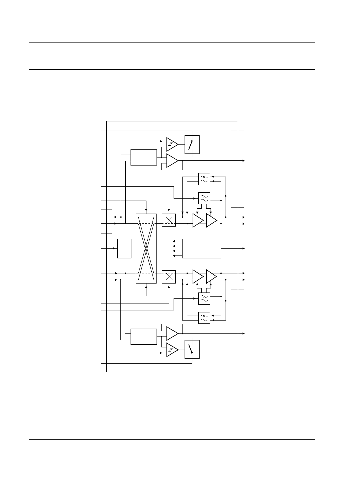
BLOCK DIAGRAM
handbook, full pagewidth
V
EE1A
LOSTH1
LEVEL1
GND1A
IN1Q
GND1A
INV1
S1
IN1
32
10
LOS
DETECTOR
TZA3019AHT
12
29
31
1
2
3
4
TZA3019AV
SWITCH
TZA3019
25
V
EE1B
1×
offset
level
A1A
A1B
27
RSSI1
24
GND1B
23
OUT1
22
OUT1Q
21
GND1B
TEST
GND2A
IN2Q
IN2
GND2A
S2
INV2
LEVEL2
LOSTH2
V
EE2A
15
DFT
8
7
6
5
30
28
13
11
9
SWITCH
LOS
DETECTOR
1×
BAND GAP
REFERENCE
A2B
A2A
level
offset
14
17
18
19
20
26
16
MGT028
V
ref
GND2B
OUT2Q
OUT2
GND2B
RSSI2
V
EE2B
Fig.1 Block diagram (TZA3019AHT and TZA3019AV).
2000 Apr 10 3
Page 4
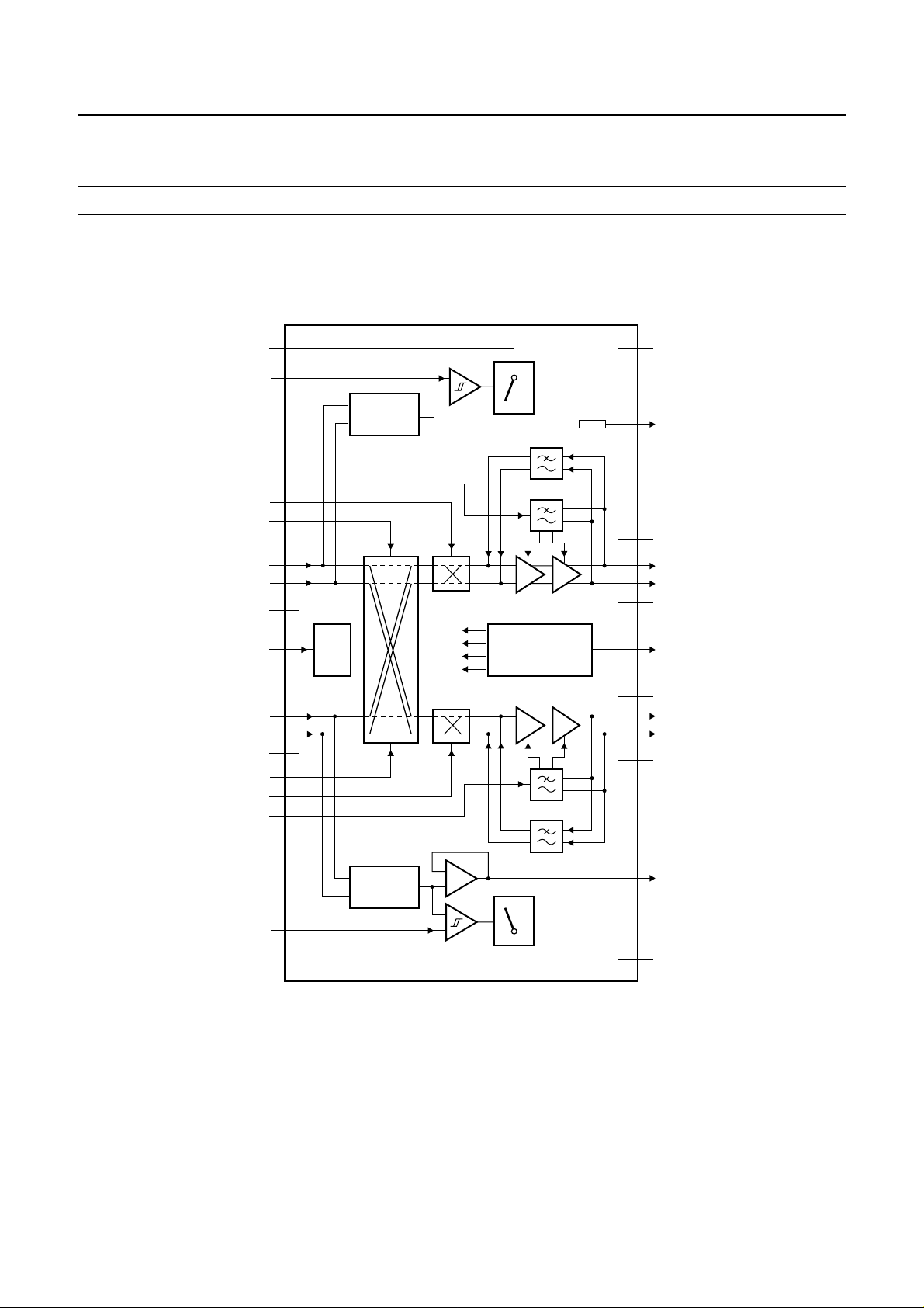
Philips Semiconductors Preliminary specification
2.5 Gbits/s dual postamplifier with level
detectors and 2 × 2 switch
handbook, full pagewidth
V
EE1A
LOSTH1
LEVEL1
GND1A
IN1Q
GND1A
INV1
S1
IN1
32
10
LOS
DETECTOR
TZA3019BHT
12
29
31
1
2
3
4
TZA3019BV
SWITCH
A1A
offset
level
A1B
5 kΩ
TZA3019
25
V
EE1B
27
LOS1
24
GND1B
23
OUT1
22
OUT1Q
21
GND1B
TEST
GND2A
IN2Q
IN2
GND2A
S2
INV2
LEVEL2
LOSTH2
V
EE2A
15
DFT
8
7
6
5
30
28
13
11
9
SWITCH
LOS
DETECTOR
1×
BAND GAP
REFERENCE
A2B
A2A
level
offset
14
17
18
19
20
26
16
MGT027
V
ref
GND2B
OUT2Q
OUT2
GND2B
RSSI2
V
EE2B
Fig.2 Block diagram (TZA3019BHT and TZA3019AV).
2000 Apr 10 4
Page 5
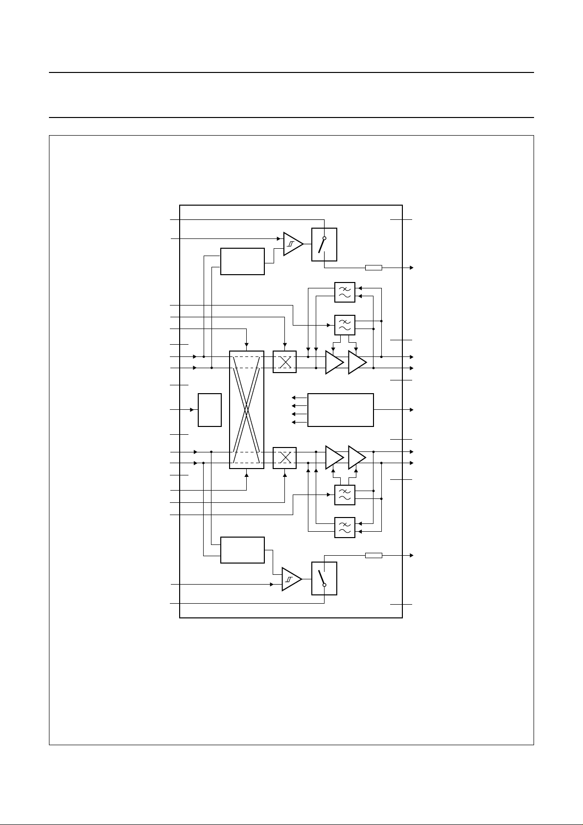
Philips Semiconductors Preliminary specification
2.5 Gbits/s dual postamplifier with level
detectors and 2 × 2 switch
handbook, full pagewidth
V
EE1A
LOSTH1
LEVEL1
GND1A
IN1Q
GND1A
INV1
S1
IN1
32
10
LOS
DETECTOR
TZA3019CHT
12
29
31
1
2
3
4
TZA3019CV
SWITCH
A1A
offset
level
A1B
5 kΩ
TZA3019
25
V
EE1B
27
LOS1
24
GND1B
23
OUT1
22
OUT1Q
21
GND1B
TEST
GND2A
IN2Q
IN2
GND2A
S2
INV2
LEVEL2
LOSTH2
V
EE2A
15
DFT
8
7
6
5
30
28
13
11
9
SWITCH
LOS
DETECTOR
BAND GAP
REFERENCE
A2B
A2A
level
offset
5 kΩ
14
17
18
19
20
26
16
MGS553
V
ref
GND2B
OUT2Q
OUT2
GND2B
LOS2
V
EE2B
Fig.3 Block diagram (TZA3019CHT and TZA3019CV).
2000 Apr 10 5
Page 6

Philips Semiconductors Preliminary specification
2.5 Gbits/s dual postamplifier with level
TZA3019
detectors and 2 × 2 switch
PINNING
PIN
SYMBOL
(1)
PAD TYPE
ABC
GND1A1111 Sground for input 1 and LOS1 circuits
IN1 2 2 2 2 I differential circuit 1 input; complimentary to pin IN1Q; DC bias level
IN1Q 3 3 3 3 I differential circuit 1 input; complimentary to pin IN1; DC bias level is
GND1A4444 Sground for input 1 and LOS1 circuits
n.c −−−5 −not connected
n.c −−−6 −not connected
GND2A5557 Sground for input 2 and LOS2 circuits
IN2 6 6 6 8 I differential circuit 2 input; complimentary to pin IN2Q; DC bias level
IN2Q 7 7 7 9 I differential circuit 2 input; complimentary to pin IN2; DC bias level is
GND2A88810 Sground for input 2 and LOS2 circuits
V
EE2A
9 9 9 11 S negative supply voltage for input 2 and LOS2 circuits
LOSTH1 10 10 10 12 I Input for level detector programming of input 1 circuit; threshold
LOSTH2 11 11 11 13 I Input for level detector programming of input 2 circuit; threshold
n.c −−−14 − not connected
LEVEL1 12 12 12 15 I Input for programming output level of output 1 circuit; output level is
LEVEL2 13 13 13 16 I Input for programming output level of output 2 circuit; output level is
V
ref
14 14 14 17 O reference voltage for level circuit and LOS threshold programming;
n.c −−−18 −
TEST 15 15 15 19 I for test purposes only; to be left open-circuit in the application
V
EE2B
16 16 16 20 S negative supply voltage for output 2 circuit
GND2B 17 17 17 21 S ground for output 2 circuit
OUT2Q 18 18 18 22 O PECL or CML compatible differential circuit 2 output;
(2)
DESCRIPTIONTZA3019xHT/xV
is set internally at approximately −0.33 V
set internally at approximately −0.33 V
is set internally at approximately −0.33 V
set internally at approximately −0.33 V
level is set by connecting external resistors between pins
GND1A and V
. When forced to V
ref
or not connected, the
EE2A
LOS1 circuit will be switched off.
level is set by connecting external resistors between pins
GND2A and V
. When forced to V
ref
or not connected, the
EE2A
LOS2 circuit will be switched off.
set by connecting external resistors between pins GND1A and V
When forced to GND1A or not connected, pins OUT1 and OUT1Q
will be switched off.
set by connecting external resistors between pins GND2A and V
When forced to GND2A or not connected, pins OUT2 and OUT2Q
will be switched off.
typical value is −1.6 V; no external capacitor allowed
complimentary to pin OUT2
ref
ref
.
.
2000 Apr 10 6
Page 7

Philips Semiconductors Preliminary specification
2.5 Gbits/s dual postamplifier with level
TZA3019
detectors and 2 × 2 switch
PIN
SYMBOL
ABC
OUT2 19 19 19 23 O PECL or CML compatible differential circuit 2 output;
GND2B 20 20 20 24 S ground for output 2 circuit
n.c −−−25 − not connected
n.c −−−26 − not connected
GND1B 21 21 21 27 S ground for output 1 circuit
OUT1Q 22 22 22 28 O PECL or CML compatible differential circuit 1 output;
OUT1 23 23 23 29 O PECL or CML compatible differential circuit 1 output;
GND1B 24 24 24 30 S ground for output 1 circuit
V
EE1B
RSSI2 26 26 − 32 O output of received signal strength indicator of detector
LOS2 −−26 33 O-DRN output loss of signal detector 2; detection of input 2 signal; direct
RSSI1 27 −−34 O output of received signal strength indicator of detector
LOS1 − 27 27 35 O-DRN output loss of signal detector 2; detection of input 2 signal; direct
INV2 28 28 28 36 TTL input to invert the signal of pins OUT2 and OUT2Q; directly positive
INV1 29 29 29 37 TTL input to invert the signal of pins OUT1 and OUT1Q; directly of
S2 30 30 30 38 TTL input selector output 2 circuit; directly positive (inverted) or negative
S1 31 31 31 39 TTL input selector output 1 circuit; directly positive (inverted) or negative
V
EE1A
V
EEP
Notes
1. The ‘x’ in TZA3019xHT/xV represents versions A, B and C.
2. Pin type abbreviations: O = output, I = input, S = power supply, TTL = logic input and O-DRN = open-drain output.
25 25 25 31 S negative supply voltage for output 1 circuit
32 32 32 40 S negative supply voltage for input 1 and LOS1 circuits
pad pad pad − S negative supply voltage pad (exposed die pad)
(1)
PAD TYPE
(2)
complimentary to pin OUT2Q
complimentary to pin OUT1
complimentary to pin OUT1Q
drive of positive or negative supplied logic via internal 5 kΩ resistor
drive of positive or negative supplied logic via internal 5 kΩ resistor
(inverted) or negative supplied logic driven
positive (inverted) or negative supplied logic driven
supplied logic driven
supplied logic driven
DESCRIPTIONTZA3019xHT/xV
2000 Apr 10 7
Page 8
Philips Semiconductors Preliminary specification
2.5 Gbits/s dual postamplifier with level
detectors and 2 × 2 switch
handbook, full pagewidth
EE1A
V
S1
S2
31
GND1A
IN1
IN1Q
GND1A
GND2A
IN2
IN2Q
GND2A
32
1
2
3
4
5
6
7
8
9
EE2A
V
30
exposed pad
TZA3019xHT
11
10
LOSTH2
LOSTH1
INV1
29
12
LEVEL1
INV2
RSSI1/LOS1
28
27
V
13
14
V
LEVEL2
RSSI2/LOS2
26
EEP
15
ref
TEST
EE1B
V
25
16
EE2B
V
24
23
22
21
20
19
18
17
MGS554
TZA3019
GND1B
OUT1
OUT1Q
GND1B
GND2B
OUT2
OUT2Q
GND2B
handbook, full pagewidth
GND1A
IN1
IN1Q
GND1A
GND2A
IN2
IN2Q
GND2A
Fig.4 Pin configuration HTQFP32.
EE1A
S1
V
1 3231302928272625
2
3
4
5
6
7
8
9
10 11 12 13 14 15
EE2A
V
LOSTH1
S2
exposed pad
TZA3019xV
LEVEL1
LOSTH2
INV1
LEVEL2
INV2
ref
V
V
EEP
RSSI1/LOS1
RSSI2/LOS2
24
23
22
21
20
19
18
17
16
TEST
EE2B
V
EE1B
V
GND1B
OUT1
OUT1Q
GND1B
GND2B
OUT2
OUT2Q
GND2B
MGT029
Fig.5 Pin configuration HBCC32.
2000 Apr 10 8
Page 9
Philips Semiconductors Preliminary specification
2.5 Gbits/s dual postamplifier with level
detectors and 2 × 2 switch
FUNCTIONAL DESCRIPTION
The TZA3019 is a dual postamplifier with multiplexer and
loss of signal detection see Figs 1, 2 and 3. The RF path
starts with the multiplexer, which connects an amplifier to
one of the two inputs. It is possible to invert the output for
easy layout of the Printed-Circuit Board (PCB). The signal
is amplified to a certain level. To guarantee this level with
minimum distortion over the temperature range and level
range, an active control part is added. The offset
compensation circuit following the inverter minimizes the
offset.
TheReceivedSignal Strength Indicator (RSSI) or the Loss
Of Signal (LOS) detection uses a 7-stage ‘successive
detection’circuit.It provides a logarithmic output. The LOS
is followed by a comparator with a programmable
threshold. The input signal level-detection is implemented
to check if the input signal voltage is above the user
programmed level. This can insure that data will only be
transmittedwhentheinputsignal-to-noiseratio is sufficient
for low bit error rate system operation. A second
offset compensation circuit minimizes the offset of the
logarithmic amplifier.
RF input circuit
TZA3019
In such cases, pull-up resistors of 100 Ω should be
connected as close as possible to the IC from
pins OUT1 and OUT1Q, and pins OUT2 and OUT2Q to
V
and V
EE1B
are not needed in most applications.
handbook, halfpage
IN1, IN2
IN1Q, IN2Q
respectively. These matching resistors
EE2B
GND1A,
GND2A
12 pF
420 Ω
50 Ω50 Ω
MGS555
V
V
Fig.6 RF input circuit.
EE1A
EE2A
,
The input circuit contains internal 50 Ω resistors
decoupled to ground via an internal common mode 12 pF
capacitor (see Fig.6).
The input pins are DC-biased at approximately −0.33 V by
an internal reference generator. The TZA3019 can be
DC-coupled, but AC-coupling is preferred. In case of
DC-coupling, the driving source must operate within the
allowableinputrange(−1.0 to +0.3 V). A DC-offset voltage
of more than a few millivolts should be avoided, since the
internal DC-offset compensation circuit has a limited
correction range. When AC-coupling is used, if no
DC-compatibility is required, the values of the coupling
capacitors must be large enough to pass the lowest input
frequency of interest. Capacitor tolerance and resistor
variation must be included for an accurate calculation.
Do not use signal frequencies around the low cut-off
circuit frequencies (f
and f
= 1 MHz for the LOS circuits).
−3dB(l)
= 50 kHz for the postamplifiers
−3dB(l)
RF output circuit
Matching the main amplifier outputs (see Fig.7) is not
mandatory. In most applications, the transmission line
receiving end will be properly matched, while very little
reflections occur.
Matching the transmitting end to absorb reflections is only
recommended for very sensitive applications.
Postamplifier level adjustment
Thepostamplifier boosts the signal up to PECL levels. The
output can be either CML- or PECL-level compatible,
adjusted by means of the voltage on pins LEVEL1
and LEVEL2.TheDC voltagesofpins OUT1 and OUT1Q,
and pins OUT2 and OUT2Q match with the DC-levels
on pins LEVEL1 and LEVEL2, respectively. Due to the
receiving end 50 Ω load resistance, it means that at the
same level of V
AC-coupling are not equal to V
o(p-p)
, V
LEVEL1
and V
LEVEL1
LEVEL2
and V
with
LEVEL2
with
DC-coupling (see Figs 7 and 8).
The postamplifier is in power-down state when pin
LEVEL1 or LEVEL2 is connected to ground or not
connected (see Fig.8).
Postamplifier DC offset cancellation loop
Offset control loops connected between the inputs of the
buffersA1Aand A2A and the outputs of the amplifiers A1B
and A2B (see Figs 1, 2 and 3) will keep the input of both
buffers at their toggle point during the absence of an input
signal.Theactiveoffset compensation circuit is integrated,
so no external capacitor is required. The loop time
constant determines the lower cut-off frequency of the
amplifier chain. The cut-off frequency of the offset
compensations is fixed internally at approximately 5 kHz.
2000 Apr 10 9
Page 10
Philips Semiconductors Preliminary specification
2.5 Gbits/s dual postamplifier with level
detectors and 2 × 2 switch
o(se)(p-p)
×=
---------------------R1 R2+
GND1A,
GND2A
R1
LEVEL1,
LEVEL2
R2
.
R1
V
100 Ω
level
100 Ω
REG
V
ref
.
LEVEL1
or V
LEVEL2=VGND
.
handbook, full pagewidth
V
= 0.5 × V
level
V
levelVref
Level detector in power-down mode: V
GND1B,
GND2B
OUT1,
OUT2
OUT1Q,
OUT2Q
V
level
V
o
(V)
TZA3019
50
50
Ω
V
o
0
Ω
V
o(se)(p-p)
MGS556
handbook, full pagewidth
GND1A,
GND2A
R1
LEVEL1,
LEVEL2
R2
V
ref
V
= 1.5 × V
level
V
levelVref
Level detector in power-down mode: V
o(se)(p-p)
×=
---------------------R1 R2+
R1
.
.
V
level
REG
LEVEL1
100 Ω
or V
LEVEL2=VGND
a. DC-coupling.
GND1B,
GND2B
100 Ω
OUT1,
OUT2
OUT1Q,
OUT2Q
.
V
level
V
o
(V)
50
50
Ω
V
o
Ω
0
V
o(se)(p-p)
MGL811
b. AC-coupling.
Fig.7 RF output configurations.
2000 Apr 10 10
Page 11

Philips Semiconductors Preliminary specification
2.5 Gbits/s dual postamplifier with level
detectors and 2 × 2 switch
handbook, full pagewidth
V
o(se)(p-p)
(mV)
1000
800
DC-coupled AC-coupled
600
400
200
0
0 100
20 40 60 80
V
level
(% of V
ref
TZA3019
MGS557
)
Fig.8 Output signal as a function of V
TTL logic input of selector and inverter
The logic levels are differently defined for positive or
negative logic (see Fig.9). It should be noted that positive
logic levels are inverted if a negative supply voltage is
used.
Outputs as a function of switch input pins S1, S2,
INV1 and INV2
See Tables 1, 2, 3 and 4.
The default values for the switch input pins S1, S2, INV1
and INV2 if not connected, is zero.
Table 1 OUT1 and OUT1Q as function of input S1
S1 OUT1 OUT1Q
0 IN1 IN1Q
1 IN2 IN2Q
.
level
Table 2 OUT2 and OUT2Q as function of input S2
S2 OUT2 OUT2Q
0 IN2 IN2Q
1 IN1 IN1Q
Table 3 OUT1 and OUT1Q as function of INV1
INV1 OUT1 OUT1Q
0 IN1 or IN2 IN1Q or IN2Q
1 IN1Q or IN2Q IN1 or IN2
Table 4 OUT2 and OUT2Q as function of INV2
INV2 OUT2 OUT2Q
0 IN1 or IN2 IN1Q or IN2Q
1 IN1Q or IN2Q IN1 or IN2
2000 Apr 10 11
Page 12

Philips Semiconductors Preliminary specification
2.5 Gbits/s dual postamplifier with level
detectors and 2 × 2 switch
handbook, full pagewidth
handbook, full pagewidth
logic
level
1
0
V
EE
−4 −3 −2 −10
2.0 V
(1)
0.8 V
1.4 V
a. Negative circuit supply voltage VEE and negative logic supply voltage VEE.
logic
level
1
2.0 V
TTL
GND
2.0 V
0.8 V
1.4 V
+1 +2 +3
2.0 V
TZA3019
MGS558
VI (V)
MGS559
(1)
handbook, full pagewidth
TTL
0.8 V
0
V
−4 −3 −2 −10
1.4 V
EE
b. Negative circuit supply voltage VEE and positive logic supply voltage VCC.
logic
level
1
2.0 V
(1)
GND
0.8 V
1.4 V
+1 +2 +3
2.0 V
VI (V)
MGS560
V
CC
TTL
0.8 V
0
GND
−10
1.4 V
+1 +2 +3 +4
c. Positive circuit supply voltage VCC and positive logic supply voltage VCC.
0.8 V
1.4 V
V
CC
+5 +6
VI (V)
(1) Level not defined.
Fig.9 Logic levels on pins S1, S2, INV1 and INV2 as a function of the input voltages.
2000 Apr 10 12
Page 13

Philips Semiconductors Preliminary specification
2.5 Gbits/s dual postamplifier with level
detectors and 2 × 2 switch
RSSI and LOS detection
The TZA3019 allows AC-signal level detection. This can
prevent the outputs from reacting to noise during the
absence of a valid input signal, and can insure that data
only will be transmitted when the signal-to-noise ratio of
the input signal is sufficient to insure low bit error rate
system operation.
TheRSSIdetection circuit uses seven limiting amplifiers in
a ‘successive detection’ topology to closely approximate
logarithmic response over a total range of 70 dB. The
detectors provide full-wave rectification of the AC signals
presented at each previous amplifier stage. Their outputs
arecurrentdrivers.Eachcellincorporatesalow-pass filter,
being the first step in recovering the average value of the
demodulated signal of the input frequency. The summed
detector output currents are converted to a voltage by an
internal load resistor. This voltage is buffered and
available in the A and B versions of the TZA3019. When
V
is used V
RSSI
preventthe LOS comparator from switching tothe standby
mode. The LOS comparator detects an input signal above
a fixed threshold, resulting in a LOW-level at the LOS
circuit output.The threshold level is determined by the
voltage on pins LOSTH1 or LOSTH2 (see Fig.10). A filter
with a time constant of 1 µs nominal is included to prevent
noise spikes from triggering the level detector.
The comparator (with internal 3 dB hysteresis) drives an
open-drain circuit with an internal resistor (5 kΩ) for direct
interfacing to positive or negative logic (see Fig.11). Only
available in the B and C versions of the TZA3019.
The response is independent of the sign of theinput signal
because of the particular way the circuit has been built.
This is part of the demodulating nature of the detector,
which results in an alternating input voltage being
transformed to a rectified and filtered quasi DC-output
signal. For the TZA3019 the logarithmic voltage slope is
ϕ = 1/13 dB/mV and is essentially temperature and supply
independent through four feedback loops in the reference
circuit. The internal LOS detector output voltage is based
on V
. The demodulator characteristic depends on the
ref
waveform and the response depends roughly on the input
signal RMS value. This influences high frequencies, a
square wave input of 2.4 GHz (LOS circuit bandwidth
of 2.4 GHz) offsets the intercept voltage by 20%. V
can be calculated using the following formulae:
V
LOSTH
V
RSSI
where S = sensitivity.
must be connected to GND to
LOSTH
S 20log
×==
Vi 18µV⁄()
LOSTH
(1)
TZA3019
handbook, halfpage
V
(1) PRBS pattern input signal with a frequency <1 GHz.
(2) Linearity error typically 0.5 dB.
(3) ϕ = 1/12.5 dB/mV.
Afull understanding of the offset control loop isuseful.The
primary purpose of the loop is to extend the lower end of
the dynamic range in any case where the offset voltage of
the first stage might be high enough to cause later stages
to prematurely enter limiting, caused by the high DC-gain
of the amplifier system. The offset is automatically and
continuously compensated via a feedback path from the
last stage. An offset at the output of the logarithmic
converter is equivalent to a change of amplitude at the
input. Consequently, with DC-coupling, signal absence,
either LOW-level or HIGH-level is detected as a full signal,
only signals with an average value equal to zero give zero
output.
VersionBcanbeusedforanautofunction,whichswitches
the strongest input signal to output 1 and the weakest to
output 2. To achieve this output V
the reference voltage for input V
LOS1 can switch S1 and S2.
3
10
i(se)(p-p)
(mV)
2
10
10
1
−1
10
10
−0.16
LOS1,
LOS2
LOW-level
(3)
V
LOSTH1
, V
Fig.10 Loss of signal assert level.
LOSTH
(1)
(2)
LOS1,
LOS2
HIGH-level
50
6020 40
(% of V
LOSTH2
−0.8−0.64−0.48−0.32 −0.96 −1.12
V
, V
RSSI1
RSSI2
must be used as
RSSI2
. Then the output
MGS564
ref
(V)
7030
)
Example: a 200 mV (p-p) single-ended 1.2 GB/s PRBS
signal has an RSSI from 1003 mV.
2000 Apr 10 13
Page 14

Philips Semiconductors Preliminary specification
2.5 Gbits/s dual postamplifier with level
detectors and 2 × 2 switch
56 kΩ
I
MGS561
GND
LOS
V
EE
TZA3019
5 kΩ
handbook, halfpage
a. Negative supply and negative logic.
TZA3019
5 kΩ
LOS1,
LOS2
GND1A,
GND2A
handbook, halfpage
handbook, halfpage
GND
b. Negative supply and positive logic.
LOS1,
LOS2
GND1A,
GND2A
TZA3019
V
CC
56 kΩ
5 kΩ
LOS1,
LOS2
GND1A,
GND2A
TZA3019
V
CC
5.6 kΩ
I
LOS
V
EE
MGS562
VCC− VEE<7V.
c. Positive supply and positive logic.
Fig.11 Loss of signal outputs, pins LOS1 and LOS2.
Supply current
For the supply currents I
EE1B
and I
, see Fig.12.
EE2B
Using a positive supply voltage
Although the TZA3019 has been designed to use a single
−3.3 V supply voltage (see Fig.13), a +3.3 V supply
(see Fig.14) can also be used. However, care should be
taken with respect to RF transmission lines. The on-chip
signals refer to the various ground pins as being positive
supply pins in a +3.3 V application. The external
transmission lines will most likely be referred to the
pins V
EE1A,VEE2A,VEE1B
and V
, being the system
EE2B
ground. The RF signals will change from one reference
plane to another when interfacing the RF inputs and
outputs. A positive supply application is very vulnerable to
interference with respect to this point. For a successful
+3.3 V application, special care should be taken when
designing the PCB layout in order to reduce the influence
of interference and to keep the positive supply voltage as
clean as possible.
I
LOS
GND
MGS563
(1)
(V)
I
EE1B,
I
EE2B
(mA)
(1) I
EE1B
60
50
40
30
20
10
58
17
5
0
0 0.80.2
and I
at 25 °C.
EE2B
0.5
V
o(se)(p-p)
Fig.12 Supply current as a function of output
voltage
1
MGS566
2000 Apr 10 14
Page 15

Philips Semiconductors Preliminary specification
2.5 Gbits/s dual postamplifier with level
TZA3019
detectors and 2 × 2 switch
LIMITING VALUES
In accordance with the Absolute Maximum Rating System (IEC 60134).
SYMBOL PARAMETER MIN. MAX. UNIT
V
EE
V
n
I
n
P
tot
T
stg
T
j
T
amb
negative supply voltage −5.5 +0.5 V
DC voltage
pins IN1, IN1Q, IN2, IN2Q, LOSTH1, LOSTH2, LEVEL1, LEVEL2,
V
, TEST, OUT2Q, OUT2, OUT1Q, OUT1, V
ref
, GND1A,
EEP
VEE− 0.5 0.5 V
GND2A, GND1B and GND2B
pins LOS1, LOS2, INV1, INV2, S1 and S2 V
− 0.5 VEE+7 V
EE
DC current
pins IN1, IN1Q, IN2 and IN2Q −20 +20 mA
pins LOSTH1, LOSTH2, LEVEL1 and LEVEL2 0 14 µA
pins V
TEST, LOS1 and LOS2 −1+1mA
ref,
pins OUT1, OUT1Q, OUT2 and OUT2Q −30 +30 mA
pins INV1, INV2, S1 and S2 0 20 µA
total power dissipation − 1.2 W
storage temperature −65 +150 °C
junction temperature − 150 °C
ambient temperature −40 +85 °C
THERMAL CHARACTERISTICS
SYMBOL PARAMETER CONDITIONS VALUE UNIT
R
th(j-s)
thermal resistance from junction to
15 K/W
solder point (exposed die pad); note 1
R
th(j-a)
thermal resistance from junction to
1s2p multi-layer test board 33 K/W
ambient; note 1
R
th(s-a)
thermal resistance from solder point to
1s2p multi-layer test board 18 K/W
ambient (exposed die pad); note 1
R
th(s-a)(req)
required thermal resistance from
solder point to ambient
LOS circuits switched on
V
= 200 mV (p-p) single-ended;
o
60 K/W
both output circuits
V
= 800 mV (p-p) single-ended;
o
30 K/W
both output circuits
Note
1. JEDEC standard.
2000 Apr 10 15
Page 16

Philips Semiconductors Preliminary specification
2.5 Gbits/s dual postamplifier with level
TZA3019
detectors and 2 × 2 switch
CHARACTERISTICS
Typical values at T
temperature range and supply voltage range; all voltages referenced to ground; unless otherwise specified; note 1.
SYMBOL PARAMETER CONDITIONS MIN. TYP. MAX. UNIT
Supply
UPPLY PINS V
S
V
EE
I
EE1A
I
EE2A
I
EE1B
I
EE2B
P
tot
,
,
EE1A,VEE1B,VEE2A
negative supply voltage −3.13 −3.3 −3.47 V
negative supply current LOS circuit power-down 14 24 34 mA
negative supply current amplifier power-down 2 6 10 mA
total power dissipation power-down 100 200 300 mW
TC temperature coefficient LOS circuit switched on; I
T
j
T
amb
junction temperature −40 − +125 °C
ambient temperature −40 +25 +85 °C
Inputs multiplexer and loss of signal detector
=25°C and VEE= −3.3 V; minimum and maximum values are valid over the entire ambient
amb
AND V
EE2B
LOS circuit switched on 24 40 56 mA
V
= 200 mV (p-p)
o
11 17 24 mA
single-ended; one output
circuit
V
= 800 mV (p-p)
o
47 60 77 mA
single-ended; one output
circuit
both LOS circuits switched on
Vo= 200 mV (p-p)
220 380 555 mW
single-ended; both output
circuits
V
= 800 mV (p-p)
o
450 660 925 mW
single-ended; both output
circuits
;
30 50 80 µA/°C
EE1A
I
EE2A
V
= 800 mV (p-p)
o
single-ended; I
EE1A
; I
EE2A
15 30 50 µA/°C
PECL OR CML INPUT PINS IN1, IN1Q, IN2 AND IN2Q
V
i(p-p)
input voltage swing
single-ended; note 2 50 − 500 mV
(peak-to-peak value)
V
V
i(bias)
I
DC input bias voltage −0.28 −0.33 −0.4 V
DC and AC input window
note 3 −1.0 − +0.3 V
voltage
R
i
C
i
input resistance single-ended 35 50 70 Ω
input capacitance single-ended; note 3 0.6 0.8 1.2 pF
2000 Apr 10 16
Page 17

Philips Semiconductors Preliminary specification
2.5 Gbits/s dual postamplifier with level
TZA3019
detectors and 2 × 2 switch
SYMBOL PARAMETER CONDITIONS MIN. TYP. MAX. UNIT
Postamplifier
AMPLIFIERS A1A, A1B, A2A AND A2B
G
v
small signal voltage gain Vo= 200 mV (p-p)
single-ended; note 4
= 800 mV (p-p)
V
o
single-ended; note 4
f
D
f
−3dB(l)
signal path data rate notes 5 and 9 − 2500 − Mbits/s
low −3 dB cut-off frequency
note 3 2 5 10 kHz
DC compensation
f
−3dB(h)
t
PD
∆t
PD
high −3 dB cut-off frequency − 2.0 − GHz
propagation delay note 3 150 200 250 ps
propagation delay
difference
at the same signal levels;
note 3
J total jitter 20 bits of the 28.5kbits
pattern; notes 3 and 6
α
ct
crosstalk crosstalk of IC only 90 110 − dB
PECL OR CML OUTPUT PINS OUT1, OUT1Q, OUT2 AND OUT2Q
V
o(se)(p-p)
single-ended output voltage
50 Ω load 200 − 800 mV
(peak-to-peak value)
TC temperature coefficient
output level
t
r
t
f
R
o
C
o
rise time 20% to 80%; note 5 − 80 − ps
fall time 80% to 20%; note 5 − 80 − ps
output resistance single-ended 70 100 130 Ω
output capacitance single-ended; note 3 0.6 0.8 1.2 pF
LEVEL CONTROL INPUT PINS LEVEL1 AND LEVEL2
V
i
R
i
input voltage V
input resistance measured to
GND1A or GND2A
Multiplexer and inverter switch
10 15 19 dB
22 29 34 dB
− 05ps
− 8 − ps
−1 0 −1 mV/K
ref
− 0V
150 350 600 kΩ
PECL OR CML INPUT PINS IN1, IN1Q, IN2 AND IN2Q
α
OS(red)
input offset reduction Vo= 200 mV (p-p)
4 9 13 dB
single-ended; note 7
V
= 800 mV (p-p)
o
10 14 20 dB
single-ended; note 7
V
io(cor)
V
n(i)(eq)(rms)
input offset voltage
correction range
equivalent input noise
voltage (RMS value)
peak-to-peak value
single-ended
Vo= 800 mV (p-p)
single-ended; note 3
−10 − +10 mV
− 75 170 µV
Fn noise factor note 3 − 512dB
2000 Apr 10 17
Page 18

Philips Semiconductors Preliminary specification
2.5 Gbits/s dual postamplifier with level
TZA3019
detectors and 2 × 2 switch
SYMBOL PARAMETER CONDITIONS MIN. TYP. MAX. UNIT
SWITCH CIRCUIT
t
a
t
d
TTL INPUT PINS S1, S2, INV1 AND INV2
V
IL
V
IH
R
i
I
i
Received Signal Strength Indicator and Loss Of Signal detector
RSSI AND LOS CIRCUIT
V
i(se)(p-p)
DR dynamic range 57 60 63 dB
S
LOS
TC
sens
LE linearity error see Fig.10 − 0.5 1 dB
α
OS(red)
V
io(cor)
f
−3dB(l)
f
−3dB(h)
LOS CIRCUIT
hys
LOS
t
a
t
d
INPUT PINS LOSTH1 AND LOSTH2
V
i
R
i
assert time multiplexer and inverter 70 100 200 ns
de-assert time multiplexer and inverter 55 80 160 ns
LOW-level input voltage positive logic 2.0 − VEE+ 7.3 V
negative logic V
− 0.3 −−2.5 V
EE
HIGH-level input voltage negative logic −1.3 − +0.3 V
positive logic −0.3 − +0.8 V
input resistance measured to V
EE1A
or V
EE2A
100 180 400 kΩ
input current −10 − +10 µA
single-ended input voltage
0.4 − 400 mV
swing (peak-to-peak value)
LOS sensitivity 50 MHz, square; note 8 11 12.5 14 mV/dB
620 MHz, square; note 8 10.7 11.9 13 mV/dB
1.2 GHz, square; note 8 10 11.1 12.2 mV/dB
100 MB/s PRBS (2
− 1);
11.2 12.7 14.2 mV/dB
31
note 8
1.2 GB/s PRBS (2
31
− 1);
10.9 12.4 13.9 mV/dB
note 8
100 GB/s PRBS (2
31
−1);
10.7 11.9 13 mV/dB
note 8
temperature coefficient
−20 −2µV/dbK
sensitivity
input offset reduction notes 3 and 7 25 35 45 dB
input offset voltage
correction range
peak-to-peak value
single-ended
−5 − +5 mV
low −3 dB cut-off frequency 0.5 1 2 MHz
high −3 dB cut-off frequency note 8 1.5 2 2.5 GHz
LOS hysteresis input signal waveform
2.0 3.0 4.0 dB
dependency
assert time note 3 −−5µS
de-assert time note 3 −−5µS
input voltage V
input resistance measured to V
EE1A
or V
EE2A
EE
150 350 600 kΩ
− 0V
2000 Apr 10 18
Page 19

Philips Semiconductors Preliminary specification
2.5 Gbits/s dual postamplifier with level
TZA3019
detectors and 2 × 2 switch
SYMBOL PARAMETER CONDITIONS MIN. TYP. MAX. UNIT
OUTPUT PINS LOS1 AND LOS2
V
o
I
o(sink)
R
o
output voltage V
EE
output sink current −−1mA
output resistance internal output series
3.5 5 6.5 kΩ
resistance
OUTPUT PINS RSSI1 AND RSSI2
V
o
I
o
output voltage −1 − 0V
output current −1 − +1 mA
Band gap reference circuit
OUTPUT PIN V
V
ref
C
ext
REF
reference voltage −1.45 −1.6 −1.8 V
allowed external
−−10 pF
capacitance
I
o(sink)
output sink current −−500 µA
Notes
1. It is assumed that both CML inputs carry a complementary signal with the specified peak-to-peak value (true
differential excitation).
2. Minimum signal with limiting output.
3. Guaranteed by design.
− 3.5 V
V
4. GV=
-----V
o
i
5. Based on −3dB cut-off frequency.
6. Vi= 100 mV (p-p) single-ended and Vo= 200 mV (p-p) single-ended.
G
7. Input offset reduction =
AC
----------G
DC
8. Sensitivity depends on the waveform and is therefore a function of −3 dB cut-off frequency see equation (1).
9. Low limit can go as low as DC if input signal overrides input offset voltage correction range.
APPLICATION INFORMATION
RF input and output connections
Striplines, or microstrips, with an odd mode characteristic
impedance of Zo=50Ω must be used for the differential
RF connectionsonthePCB.Thisapplies to both the signal
inputs and the signal outputs. The two lines in each pair
should have the same length.
All VEEpins (one at each corner and the exposed die pad)
need to be connected to a common supply plane with an
inductance as low as possible. This plane should be
decoupled to ground. To avoid high frequency resonance,
multiple bypass capacitors should not be mounted at the
same location. To minimize low frequency switching noise
inthevicinityof the TZA3019, the power supply line should
be filtered once using a beaded capacitor circuit with a low
cut-off frequency (see Figs 13 and 14).
Grounding and power supply decoupling
The ground connection on the PCB needs to be a large
copper filled area connected to a common ground plane
The VEE connection on the PCB also needs to be a large
copper area to improve heat transfer to the PCB and thus
support IC cooling.
with an inductance as low as possible.
2000 Apr 10 19
Page 20

Philips Semiconductors Preliminary specification
2.5 Gbits/s dual postamplifier with level
detectors and 2 × 2 switch
handbook, full pagewidth
012345mm
To central
VEE decoupling
GND1A
IN1
IN1Q
GND1A
GND2A
IN2
IN2Q
87654321
GND2A
Boundary of 200 mm2 area
0603
V
EE1A
S1
32
0603 0603
31
INV2
INV1
S2
30
LOS1
29
28
27
LOS2
26
V
EE1B
25
To central
V
decoupling
EE
1718192021222324
0603
GND1B
OUT1
OUT1Q
GND1B
GND2B
OUT2
OUT2Q
GND2B
GND
TZA3019
EEP
signal/V
VEEGND
9
10
11
12
13
14
15
0603
0603
V
EE2A
LOSTH1
LOSTH2
LEVEL1
LEVEL2
16
V
V
TEST
EE2B
ref
0603
0603
06030603
To central
VEE decoupling
06030603
To central
V
decoupling
EE
06030603
06030603
060306030603
HTQFP
In order to enable heat flow out of the package, the following measures have to be taken:
(1) Solder the 3 × 3 mm2 die pad to a plane with maximum size.
(2) Add a plane with minimum 200 mm2 in an inner layer, surrounded by ground layers.
(3) Use maximum amount of vias to connect two planes.
(4) Use minimum of openings in heat transport area between hot plane and ground planes.
Fig.13 PCB layout for negative supply voltage.
MGS567
2000 Apr 10 20
Page 21

Philips Semiconductors Preliminary specification
2.5 Gbits/s dual postamplifier with level
detectors and 2 × 2 switch
handbook, full pagewidth
012345mm
To central
VEE decoupling
0603
GND1A
IN1
IN1Q
GND1A
GND2A
IN2
IN2Q
87654321
GND2A
Boundary of 200 mm2 area
LOS1
INV2
V
EE1A
32
0603 0603
INV1
S1
S2
31
30
29
28
27
LOS2
26
V
EE1B
25
To central
V
decoupling
EE
GND1B
OUT1
OUT1Q
GND1B
GND2B
OUT2
OUT2Q
1718192021222324
GND2B
0603
GND
TZA3019
EEP
signal/V
VEEGND
16
14
15
V
V
TEST
EE2B
ref
0603
0603
0603
0603
9
V
EE2A
10
LOSTH1
11
LOSTH2
12
LEVEL1
13
LEVEL2
06030603
To central
VEE decoupling
06030603
To central
VEE decoupling
06030603
06030603
0603 HTQFP06030603
In order to enable heat flow out of the package, the following measures have to be taken:
(1) Solder the 3 × 3 mm2 die pad to a plane with maximum size.
(2) Add a plane with minimum 200 mm2 in an inner layer, surrounded by ground layers.
(3) Use maximum amount of vias to connect two planes.
(4) Use minimum of openings in heat transport area between hot plane and ground planes.
Fig.14 PCB layout for positive supply voltage.
MGS568
2000 Apr 10 21
Page 22

Philips Semiconductors Preliminary specification
2.5 Gbits/s dual postamplifier with level
detectors and 2 × 2 switch
BONDING PAD LOCATIONS
SYMBOL PAD
COORDINATES
xy
GND1A 1 −928 +710
IN1 2 −928 +553
IN1Q 3 −928 +396
GND1A 4 −928 +239
n.c. 5 −928 +81
n.c. 6 −928 −81
GND2A 7 −928 −239
IN2 8 −928 −396
IN2Q 9 −928 −553
GND2A 10 −928 −710
V
EE2A
11 −707 −928
LOSTH1 12 −550 −928
LOSTH2 13 −393 −928
n.c. 14 −236 −928
LEVEL1 15 −79 −928
LEVEL2 16 +79 −928
VREF 17 +236 −928
n.c. 18 +393 −928
TEST 19 +550 −928
V
EE2B
20 +707 −928
GND2B 21 +928 −710
OUT2Q 22 +928 −553
(1)
TZA3019
SYMBOL PAD
COORDINATES
xy
OUT2 23 +928 −396
GND2B 24 +928 −239
n.c. 25 +928 −81
n.c. 26 +928 +81
GND1B 27 +928 +239
OUT1Q 28 +928 +396
OUT1 29 +928 +553
GND1B 30 +928 +710
V
EE1B
31 +707 +928
RSSI2 32 +550 +928
LOS2 33 +393 +928
RSSI1 34 +236 +928
LOS1 35 +79 +928
INV2 36 −79 +928
INV1 37 −236 +928
S2 38 −393 +928
S1 39 −550 +928
V
EE1A
40 −707 +928
Note
1. All x and y coordinates represent the position of the
centreofthepadin µm with respect to the centre of the
die (see Fig.15)
(1)
2000 Apr 10 22
Page 23

Philips Semiconductors Preliminary specification
2.5 Gbits/s dual postamplifier with level
detectors and 2 × 2 switch
handbook, full pagewidth
EE1A
GND1A
IN1
IN1Q
GND1A
n.c.
n.c.
GND2A
IN2
IN2Q
GND2A
V
40 39 38 37 36 35 34 33 32 31
1
2
3
4
5
6
7
8
9
10
11 12 13 14 15 16 17 18 19 20
EE2A
V
S1
S2
x
LOSTH2
LOSTH1
INV1
TZA3019U
n.c.
INV2
0
0
y
LEVEL1
RSSI1
LOS1
ref
V
LEVEL2
LOS2
n.c.
RSSI2
V
TEST
V
EE1B
30
29
28
27
26
25
24
23
22
21
EE2B
TZA3019
GND1B
OUT1
OUT1Q
GND1B
n.c.
n.c.
GND2B
OUT2
OUT2Q
GND2B
MGT030
Fig.15 Bonding pad locations TZA3019U.
2000 Apr 10 23
Page 24

Philips Semiconductors Preliminary specification
2.5 Gbits/s dual postamplifier with level
detectors and 2 × 2 switch
PACKAGE OUTLINE
HTQFP32: plastic, heatsink thin quad flat package; 32 leads; body 5 x 5 x 1.0 mm
c
y
25
E
h
32
heathsink side
pin 1 index
X
D
h
1724
Z
16
e
9
A
E
H
E
b
E
w M
p
A
2
A
A
1
TZA3019
SOT547-2
(A )
3
L
p
L
θ
81
w M
b
p
e
D
H
D
DIMENSIONS (mm are the original dimensions)
A
UNIT
mm
Note
1. Plastic or metal protrusions of 0.25 mm maximum per side are not included.
OUTLINE
VERSION
SOT547-2
A1A2A3b
max.
0.15
1.2
0.05
ceLywvθ
p
1.05
0.95
0.27
0.17
0.20
0.09
0.25
IEC JEDEC EIAJ
Z
D
B
0 2.5 5 mm
scale
D
(1)
5.1
4.9
(1)
E
D
h
5.1
3.1
4.9
2.7
REFERENCES
E
3.1
2.7
h
v M
v M
0.5
A
B
HDH
7.1
6.9
7.1
6.9
detail X
(1)
E
L
0.75
0.45
p
0.08 0.080.21.0
EUROPEAN
PROJECTION
Z
Z
D
E
0.89
0.89
0.61
0.61
ISSUE DATE
99-06-15
(1)
7°
0°
2000 Apr 10 24
Page 25

Philips Semiconductors Preliminary specification
2.5 Gbits/s dual postamplifier with level
detectors and 2 × 2 switch
HBCC32: plastic, heatsink bottom chip carrier; 32 terminals; body 5 x 5 x 0.65 mm
E
x
B
b
1
b
2
detail X
x
C
vA
ball A1
index area
C
B
e
e
D
1
A
TZA3019
SOT560-1
M
w
M
w
b
b
3
M
w
M
w
y
e
2
1
32
DIMENSIONS (mm are the original dimensions)
A
max.
0.80
A
1bA2
0.10
0.05
0.70
0.35
0.60
0.20
IEC JEDEC EIAJ
UNIT
mm
OUTLINE
VERSION
SOT560-1 MO-217
b
0.50
0.30
D
1
e
3
b
1
2
0.50
0.35
e4E
1
X
0 2.5 5 mm
scale
5.1
4.9
E
E
1
3.2
0.5
3.0
D
b
3
5.1
0.50
4.9
0.35
REFERENCES
D
3.2
3.0
1
4.2
A
1
A
2
A
e
e
1
2
4.2
e
e
4
3
4.15
4.15
EUROPEAN
PROJECTION
we
v
0.15 0.15 0.05
0.2
ISSUE DATE
xy
99-09-10
00-02-01
2000 Apr 10 25
Page 26

Philips Semiconductors Preliminary specification
2.5 Gbits/s dual postamplifier with level
detectors and 2 × 2 switch
SOLDERING
Introduction to soldering surface mount packages
Thistextgivesaverybriefinsighttoacomplextechnology.
A more in-depth account of soldering ICs can be found in
our
“Data Handbook IC26; Integrated Circuit Packages”
(document order number 9398 652 90011).
There is no soldering method that is ideal for all surface
mount IC packages. Wave solderingis not always suitable
for surface mount ICs, or for printed-circuit boards with
high population densities. In these situations reflow
soldering is often used.
Reflow soldering
Reflow soldering requires solder paste (a suspension of
fine solder particles, flux and binding agent) to be applied
totheprinted-circuit board by screen printing, stencilling or
pressure-syringe dispensing before package placement.
Several methods exist for reflowing; for example,
infrared/convection heating in a conveyor type oven.
Throughput times (preheating, soldering and cooling) vary
between 100 and 200 seconds depending on heating
method.
Typical reflow peak temperatures range from
215 to 250 °C. The top-surface temperature of the
packages should preferable be kept below 230 °C.
TZA3019
• Use a double-wave soldering method comprising a
turbulent wave with high upward pressure followed by a
smooth laminar wave.
• For packages with leads on two sides and a pitch (e):
– larger than or equal to 1.27 mm, the footprint
longitudinal axis is preferred to be parallel to the
transport direction of the printed-circuit board;
– smaller than 1.27 mm, the footprint longitudinal axis
must be parallel to the transport direction of the
printed-circuit board.
The footprint must incorporate solder thieves at the
downstream end.
• Forpackageswithleadsonfoursides,thefootprintmust
be placed at a 45° angle to the transport direction of the
printed-circuit board. The footprint must incorporate
solder thieves downstream and at the side corners.
During placement and before soldering, the package must
be fixed with a droplet of adhesive. The adhesive can be
applied by screen printing, pin transfer or syringe
dispensing. The package can be soldered after the
adhesive is cured.
Typical dwell time is 4 seconds at 250 °C.
A mildly-activated flux will eliminate the need for removal
of corrosive residues in most applications.
Manual soldering
Wave soldering
Conventional single wave soldering is not recommended
forsurfacemountdevices(SMDs)orprinted-circuitboards
with a high component density, as solder bridging and
non-wetting can present major problems.
To overcome these problems the double-wave soldering
method was specifically developed.
If wave soldering is used the following conditions must be
observed for optimal results:
Fix the component by first soldering two
diagonally-opposite end leads. Use a low voltage (24 V or
less) soldering iron applied to the flat part of the lead.
Contact time must be limited to 10 seconds at up to
300 °C.
When using a dedicated tool, all other leads can be
soldered in one operation within 2 to 5 seconds between
270 and 320 °C.
2000 Apr 10 26
Page 27

Philips Semiconductors Preliminary specification
2.5 Gbits/s dual postamplifier with level
TZA3019
detectors and 2 × 2 switch
Suitability of surface mount IC packages for wave and reflow soldering methods
PACKAGE
BGA, SQFP not suitable suitable
HLQFP, HSQFP, HSOP, HTQFP, HTSSOP, SMS not suitable
(3)
PLCC
LQFP, QFP, TQFP not recommended
SSOP, TSSOP, VSO not recommended
Notes
1. All surface mount (SMD) packages are moisture sensitive. Depending upon the moisture content, the maximum
2. Thesepackages are not suitable for wave soldering as a solder joint between the printed-circuit board and heatsink
3. If wave soldering is considered, then the package must be placed at a 45° angle to the solder wave direction.
4. Wavesoldering is only suitable for LQFP, TQFP and QFP packages with a pitch (e) equal to or larger than 0.8 mm;
5. Wavesolderingis only suitable for SSOP and TSSOP packages with a pitch (e) equal to or larger than 0.65 mm; it is
, SO, SOJ suitable suitable
temperature (with respect to time) and body size of the package, there is a risk that internal or external package
cracks may occur due to vaporization of the moisture in them (the so called popcorn effect). For details, refer to the
Drypack information in the
(at bottom version) can not be achieved, and as solder may stick to the heatsink (on top version).
The package footprint must incorporate solder thieves downstream and at the side corners.
it is definitely not suitable for packages with a pitch (e) equal to or smaller than 0.65 mm.
definitely not suitable for packages with a pitch (e) equal to or smaller than 0.5 mm.
“Data Handbook IC26; Integrated Circuit Packages; Section: Packing Methods”
WAVE REFLOW
(2)
SOLDERING METHOD
suitable
(3)(4)
(5)
suitable
suitable
(1)
.
2000 Apr 10 27
Page 28

Philips Semiconductors Preliminary specification
2.5 Gbits/s dual postamplifier with level
TZA3019
detectors and 2 × 2 switch
DATA SHEET STATUS
DATA SHEET STATUS
Objective specification Development This data sheet contains the design target or goal specifications for
Preliminary specification Qualification This data sheet contains preliminary data, and supplementary data will be
Product specification Production This data sheet contains final specifications. Philips Semiconductors
Note
1. Please consult the most recently issued data sheet before initiating or completing a design.
DEFINITIONS
Short-form specification The data in a short-form
specification is extracted from a full data sheet with the
same type number and title. For detailed information see
the relevant data sheet or data handbook.
Limiting values definition Limiting values given are in
accordance with the Absolute Maximum Rating System
(IEC 60134). Stress above one or more of the limiting
values may cause permanent damage to the device.
These are stress ratings only and operation of the device
attheseoratanyotherconditionsabovethosegiveninthe
Characteristics sections of the specification is not implied.
Exposure to limiting values for extended periods may
affect device reliability.
Application information Applications that are
described herein for any of these products are for
illustrative purposes only. Philips Semiconductors make
norepresentationorwarrantythatsuchapplicationswill be
suitable for the specified use without further testing or
modification.
PRODUCT
STATUS
DEFINITIONS
product development. Specification may change in any manner without
notice.
published at a later date. Philips Semiconductors reserves the right to
make changes at any time without notice in order to improve design and
supply the best possible product.
reserves the right to make changes at any time without notice in order to
improve design and supply the best possible product.
DISCLAIMERS
Life support applications These products are not
designed for use in life support appliances, devices, or
systems where malfunction of these products can
reasonably be expected to resultin personal injury. Philips
Semiconductorscustomersusingorsellingtheseproducts
for use in such applications do so at their own risk and
agree to fully indemnify Philips Semiconductors for any
damages resulting from such application.
Right to make changes Philips Semiconductors
reserves the right to make changes, without notice, in the
products, including circuits, standard cells, and/or
software, described or contained herein in order to
improve design and/or performance. Philips
Semiconductors assumes no responsibility or liability for
theuseofanyoftheseproducts,conveysnolicenceortitle
under any patent, copyright, or mask work right to these
products,andmakesnorepresentations or warranties that
these products are free from patent, copyright, or mask
work right infringement, unless otherwise specified.
(1)
2000 Apr 10 28
Page 29

Philips Semiconductors Preliminary specification
2.5 Gbits/s dual postamplifier with level
detectors and 2 × 2 switch
NOTES
TZA3019
2000 Apr 10 29
Page 30

Philips Semiconductors Preliminary specification
2.5 Gbits/s dual postamplifier with level
detectors and 2 × 2 switch
NOTES
TZA3019
2000 Apr 10 30
Page 31

Philips Semiconductors Preliminary specification
2.5 Gbits/s dual postamplifier with level
detectors and 2 × 2 switch
NOTES
TZA3019
2000 Apr 10 31
Page 32

Philips Semiconductors – a w orldwide compan y
Argentina: see South America
Australia: 3 Figtree Drive, HOMEBUSH, NSW 2140,
Tel. +61 2 9704 8141, Fax. +61 2 9704 8139
Austria: Computerstr. 6, A-1101 WIEN, P.O. Box 213,
Tel. +43 1 60 101 1248, Fax. +43 1 60 101 1210
Belarus: Hotel Minsk Business Center, Bld. 3, r. 1211, Volodarski Str. 6,
220050 MINSK, Tel. +375 172 20 0733, Fax. +375 172 20 0773
Belgium: see The Netherlands
Brazil: see South America
Bulgaria: Philips Bulgaria Ltd., Energoproject, 15th floor,
51 James Bourchier Blvd., 1407 SOFIA,
Tel. +359 2 68 9211, Fax. +359 2 68 9102
Canada: PHILIPS SEMICONDUCTORS/COMPONENTS,
Tel. +1 800 234 7381, Fax. +1 800 943 0087
China/Hong Kong: 501 Hong Kong Industrial Technology Centre,
72 Tat Chee Avenue, Kowloon Tong, HONG KONG,
Tel. +852 2319 7888, Fax. +852 2319 7700
Colombia: see South America
Czech Republic: see Austria
Denmark: Sydhavnsgade 23, 1780 COPENHAGEN V,
Tel. +45 33 29 3333, Fax. +45 33 29 3905
Finland: Sinikalliontie 3, FIN-02630 ESPOO,
Tel. +358 9 615 800, Fax. +358 9 6158 0920
France: 51 Rue Carnot, BP317, 92156 SURESNES Cedex,
Tel. +33 1 4099 6161, Fax. +33 1 4099 6427
Germany: Hammerbrookstraße 69, D-20097 HAMBURG,
Tel. +49 40 2353 60, Fax. +49 40 2353 6300
Hungary: see Austria
India: Philips INDIA Ltd, Band Box Building, 2nd floor,
254-D, Dr. Annie Besant Road, Worli, MUMBAI 400 025,
Tel. +91 22 493 8541, Fax. +91 22 493 0966
Indonesia: PT Philips DevelopmentCorporation, Semiconductors Division,
Gedung Philips, Jl. Buncit Raya Kav.99-100, JAKARTA 12510,
Tel. +62 21 794 0040 ext. 2501, Fax. +62 21 794 0080
Ireland: Newstead, Clonskeagh, DUBLIN 14,
Tel. +353 1 7640 000, Fax. +353 1 7640 200
Israel: RAPAC Electronics, 7 Kehilat Saloniki St, PO Box 18053,
TEL AVIV 61180, Tel. +972 3 645 0444, Fax. +972 3 649 1007
Italy: PHILIPS SEMICONDUCTORS,Via Casati, 23 - 20052 MONZA (MI),
Tel. +39 039 203 6838, Fax +39 039 203 6800
Japan: Philips Bldg 13-37, Kohnan 2-chome, Minato-ku,
TOKYO 108-8507, Tel. +81 3 3740 5130, Fax. +81 3 3740 5057
Korea: Philips House, 260-199 Itaewon-dong, Yongsan-ku, SEOUL,
Tel. +82 2 709 1412, Fax. +82 2 709 1415
Malaysia: No. 76 Jalan Universiti, 46200 PETALING JAYA, SELANGOR,
Tel. +60 3 750 5214, Fax. +60 3 757 4880
Mexico: 5900 Gateway East, Suite 200, EL PASO, TEXAS 79905,
Tel. +9-5 800 234 7381, Fax +9-5 800 943 0087
Middle East: see Italy
Netherlands: Postbus 90050, 5600 PB EINDHOVEN, Bldg. VB,
Tel. +31 40 27 82785, Fax. +31 40 27 88399
New Zealand: 2 Wagener Place, C.P.O. Box 1041, AUCKLAND,
Tel. +64 9 849 4160, Fax. +64 9 849 7811
Norway: Box 1, Manglerud 0612, OSLO,
Tel. +47 22 74 8000, Fax. +47 22 74 8341
Pakistan: see Singapore
Philippines: Philips Semiconductors Philippines Inc.,
106 Valero St. Salcedo Village, P.O. Box 2108 MCC, MAKATI,
Metro MANILA, Tel. +63 2 816 6380, Fax. +63 2 817 3474
Poland: Al.Jerozolimskie 195 B, 02-222 WARSAW,
Tel. +48 22 5710 000, Fax. +48 22 5710 001
Portugal: see Spain
Romania: see Italy
Russia: Philips Russia, Ul. Usatcheva 35A, 119048 MOSCOW,
Tel. +7 095 755 6918, Fax. +7 095 755 6919
Singapore: Lorong 1, Toa Payoh, SINGAPORE 319762,
Tel. +65 350 2538, Fax. +65 251 6500
Slovakia: see Austria
Slovenia: see Italy
South Africa: S.A. PHILIPS Pty Ltd., 195-215 Main Road Martindale,
2092 JOHANNESBURG, P.O. Box 58088 Newville 2114,
Tel. +27 11 471 5401, Fax. +27 11 471 5398
South America: Al. Vicente Pinzon, 173, 6th floor,
04547-130 SÃO PAULO, SP, Brazil,
Tel. +55 11 821 2333, Fax. +55 11 821 2382
Spain: Balmes 22, 08007 BARCELONA,
Tel. +34 93 301 6312, Fax. +34 93 301 4107
Sweden: Kottbygatan 7, Akalla, S-16485 STOCKHOLM,
Tel. +46 8 5985 2000, Fax. +46 8 5985 2745
Switzerland: Allmendstrasse 140, CH-8027 ZÜRICH,
Tel. +41 1 488 2741 Fax. +41 1 488 3263
Taiwan: Philips Semiconductors, 6F, No. 96, Chien Kuo N. Rd., Sec. 1,
TAIPEI, Taiwan Tel. +886 2 2134 2886, Fax. +886 2 2134 2874
Thailand: PHILIPS ELECTRONICS (THAILAND) Ltd.,
209/2 Sanpavuth-Bangna Road Prakanong, BANGKOK 10260,
Tel. +66 2 745 4090, Fax. +66 2 398 0793
Turkey: Yukari Dudullu, Org. San. Blg., 2.Cad. Nr. 28 81260 Umraniye,
ISTANBUL, Tel. +90 216 522 1500, Fax. +90 216 522 1813
Ukraine: PHILIPS UKRAINE, 4 Patrice Lumumba str., Building B, Floor 7,
252042 KIEV, Tel. +380 44 264 2776, Fax. +380 44 268 0461
United Kingdom: Philips Semiconductors Ltd., 276 Bath Road, Hayes,
MIDDLESEX UB3 5BX, Tel. +44 208 730 5000, Fax. +44 208 754 8421
United States: 811 East Arques Avenue, SUNNYVALE, CA 94088-3409,
Tel. +1 800 234 7381, Fax. +1 800 943 0087
Uruguay: see South America
Vietnam: see Singapore
Yugoslavia: PHILIPS, Trg N. Pasica 5/v, 11000 BEOGRAD,
Tel. +381 11 3341 299, Fax.+381 11 3342 553
For all other countries apply to: Philips Semiconductors,
International Marketing & Sales Communications, Building BE-p, P.O. Box 218,
5600 MD EINDHOVEN, The Netherlands, Fax. +31 40 27 24825
© Philips Electronics N.V. SCA
All rights are reserved. Reproduction in whole or in part is prohibited without the prior written consent of the copyright owner.
The information presented in this document does not form part of any quotation or contract, is believed to be accurate and reliable and may be changed
without notice. No liability will be accepted by the publisher for any consequence of its use. Publication thereof does not convey nor imply any license
under patent- or other industrial or intellectual property rights.
2000
Internet: http://www.semiconductors.philips.com
69
Printed in The Netherlands 403510/50/01/pp32 Date of release: 2000 Apr 10 Document order number: 9397 750 06019
 Loading...