

Page 1

INTEGRATED CIRCUITS
DATA SH EET
TZA3005H
SDH/SONET STM1/OC3 and
STM4/OC12 transceiver
Product specification
Supersedes data of 1997 Aug 05
File under Integrated Circuits, IC19
2000 Feb 17
Page 2

Philips Semiconductors Product specification
SDH/SONET STM1/OC3 and STM4/OC12
transceiver
FEATURES
• Supports STM1/OC3(155.52 Mbits/s) and STM4/OC12
(622.08 Mbits/s)
• Supports reference clock frequencies of 19.44, 38.88,
51.84 and 77.76 MHz
• Meets Bellcore, ANSI and ITU-T specifications
• Meets ITU jitter specification typically to a factor of 2.5
• Integral high-frequency PLL for clock generation
• Interface to TTL logic
• Low jitter PECL (Positive Emitter Coupled Logic)
interface
• 4 or 8-bit STM1/OC3 TTL data path
• 4 or 8-bit STM4/OC12 TTL data path
• No external filter components required
• QFP64 package
• Diagnostic and line loopback modes
• Lock detect
• LOS (Loss of Signal) input
• Low power (0.9 W typical)
• Selectable frame detection and byte realignment
• Loop timing
• Forward and reverse clocking
• Squelched clock operation
• Self-biased PECL inputs to support AC coupling.
TZA3005H
GENERAL DESCRIPTION
The TZA3005H SDH/SONET transceiver chip is a fully
integrated serialization/deserialization STM1/OC3
(155.52 Mbits/s) and STM4/OC12 (622.08 Mbits/s)
interfacedevice. It performsallnecessaryserial-to-parallel
and parallel-to-serial functions in accordance with
SDH/SONET transmission standards. It is suitable for
SONET-based applications and can be used in
conjunction with the data and clock recovery unit
(TZA3004), optical front-end (TZA3023 with TZA3034/44)
anda laser driver(TZA3001). A typicalnetworkapplication
is shown in Fig.10.
A high-frequency phase-locked loop is used for on-chip
clock synthesis, which allows a slower external transmit
reference clock to be used. A reference clock of 19.44,
38.88,51.84 or 77.76 MHzcan be usedtosupportexisting
system clocking schemes. The TZA3005H also performs
SDH/SONET frame detection.
The low jitter PECL interface ensures that Bellcore, ANSI,
and ITU-T bit-error rate requirements are satisfied.
The TZA3005H is supplied in a compact QFP64 package.
APPLICATIONS
• SDH/SONET modules
• SDH/SONET-based transmission systems
• SDH/SONET test equipment
• ATM (Asynchronous Transfer Mode) over SDH/SONET
• Add drop multiplexers
• Broadband cross-connects
• Section repeaters
• Fibre optic test equipment
• Fibre optic terminators.
ORDERING INFORMATION
TYPE
NUMBER
TZA3005H QFP64 plastic quad flat package; 64 leads (lead length 1.6 mm);
2000 Feb 17 2
NAME DESCRIPTION VERSION
body 14 × 14 × 2.7 mm
PACKAGE
SOT393-1
Page 3
Philips Semiconductors Product specification
SDH/SONET STM1/OC3 and STM4/OC12
transceiver
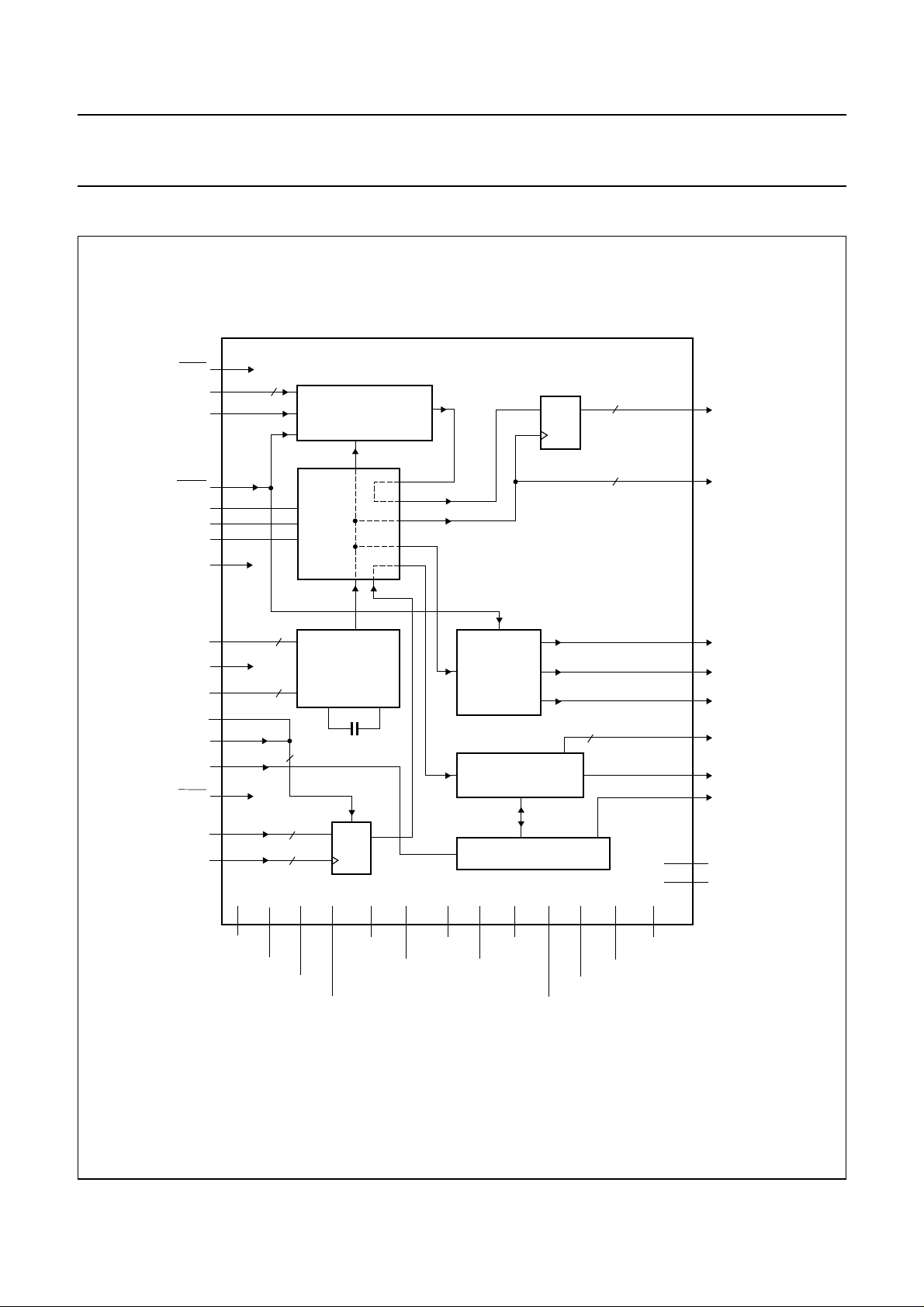
BLOCK DIAGRAM
handbook, full pagewidth
LLEN
TXPD0 to
TXPD7
TXPCLK
MRST
TEST1
TEST2
TEST3
BUSWIDTH
31
53 to 60
61
48
10
11
13
30
8
8:1 OR 4:1
P ARALLEL T O SERIAL
RF
SWITCH
BOX
TRANSMITTER
(1)
D
2
2
TZA3005H
17, 18
21, 20
TZA3005H
TXSD and
TXSDQ
TXSCLK and
TXSCLKQ
REFSEL0 and
REFSEL1
MODE
REFCLK and
REFCLKQ
SDTTL
SDPECL
OOF
DLEN
RXSD and
RXSDQ
RXSCLK and
RXSCLKQ
V
CC(SYNOUT)
3, 4
49
15, 14
22
23
33
32
24, 25
27, 28
GND
2
CLOCK
SYNTHESIZER
2
on-chip capacitor
2
2
2
D
RECEIVER
1
2 5 8, 9 6 7 16 19
V
CCD(SYN)
SYN
V
CCA(SYN)
SYNOUT
DGND
SYN
AGND
12
GND
V
CLOCK
DIVIDER
BY 4 OR BY 8
1:8 OR 1:4
SERIAL TO P ARALLEL
FRAME HEADER DETECT
26
GND
TXOUT
CC(TXOUT)
GND
V
CC(RXCORE)
8
29
V
CC(RXOUT)
RXCORE
36, 37, 39, 40,
41, 43 to 45
34, 42
38, 46
GND
RXOUT
62
63
64
47
35
52
51
SYNCLKDIV
LOCKDET
19MHZO
RXPD0 to
RXPD7
RXPCLK
FP
V
CC(TXCORE)
GND
MGS975
TXCORE
(1) Dashed lines represent normal operation mode.
Fig.1 Block diagram.
2000 Feb 17 3
Page 4

Philips Semiconductors Product specification
SDH/SONET STM1/OC3 and STM4/OC12
transceiver
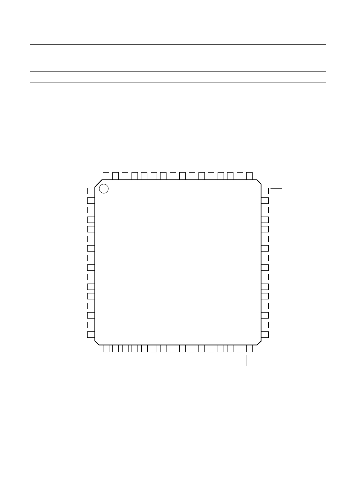
PINNING
SYMBOL PIN TYPE
V
CC(SYNOUT)
GND
SYNOUT
1 S supply voltage (synthesizer output)
2 G ground (synthesizer output)
REFSEL0 3 I reference clock select input 0
REFSEL1 4 I reference clock select input 1
DGND
V
CCD(SYN)
V
CCA(SYN)
AGND
AGND
SYN
SYN
SYN
5 G digital ground (synthesizer)
6 S digital supply voltage (synthesizer)
7 S analog supply voltage (synthesizer)
8 G analog ground (synthesizer)
9 G analog ground (synthesizer)
TEST1 10 I test and control input
TEST2 11 I test and control input
GND 12 G ground
TEST3 13 I test and control input
REFCLKQ 14 I inverted reference clock input
REFCLK 15 I reference clock input
V
CC(TXOUT)
16 S supply voltage (transmitter output)
TXSD 17 O serial data output
TXSDQ 18 O inverted serial data output
GND
TXOUT
19 G ground (transmitter output)
TXSCLKQ 20 O inverted serial clock output
TXSCLK 21 O serial clock output
SDTTL 22 I TTL signal detect input
SDPECL 23 I PECL signal detect input
RXSD 24 I serial data input
RXSDQ 25 I inverted serial data input
V
CC(RXCORE)
26 S supply voltage (receiver core)
RXSCLK 27 I serial clock input
RXSCLKQ 28 I inverted serial clock input
GND
RXCORE
29 G ground (receiver core)
BUSWIDTH 30 I 4/8 bus width select input
LLEN 31 I line loopback enable input (active LOW)
DLEN 32 I diagnostic loopback enable input (active LOW)
OOF 33 I out-of-frame enable input
GND
RXOUT
34 G ground (receiver output)
FP 35 O frame pulse output
RXPD0 36 O parallel data output 0
RXPD1 37 O parallel data output 1
V
CC(RXOUT)
38 S supply voltage (receiver output)
RXPD2 39 O parallel data output 2
RXPD3 40 O parallel data output 3
(1)
DESCRIPTION
TZA3005H
2000 Feb 17 4
Page 5

Philips Semiconductors Product specification
SDH/SONET STM1/OC3 and STM4/OC12
transceiver
SYMBOL PIN TYPE
RXPD4 41 O parallel data output 4
GND
RXOUT
RXPD5 43 O parallel data output 5
RXPD6 44 O parallel data output 6
RXPD7 45 O parallel data output 7
V
CC(RXOUT)
RXPCLK 47 O receive parallel clock output
MRST 48 I master reset (active LOW)
MODE 49 I serial data rate select STM1/STM4
ALTPIN 50 I test and control input
GND
TXCORE
V
CC(TXCORE)
TXPD0 53 I parallel data input 0
TXPD1 54 I parallel data input 1
TXPD2 55 I parallel data input 2
TXPD3 56 I parallel data input 3
TXPD4 57 I parallel data input 4
TXPD5 58 I parallel data input 5
TXPD6 59 I parallel data input 6
TXPD7 60 I parallel data input 7
TXPCLK 61 I transmit parallel clock input
SYNCLKDIV 62 O transmit byte/nibble clock output (synchronous)
LOCKDET 63 O lock detect output
19MHZO 64 O 19 MHz reference clock output
42 G ground (receiver output)
46 S supply voltage (receiver output)
51 G ground (transmitter core)
52 S supply voltage (transmitter core)
(1)
DESCRIPTION
TZA3005H
Note
1. Pin type abbreviations: O = Output, I = Input, S = Supply, G = Ground.
2000 Feb 17 5
Page 6
Philips Semiconductors Product specification
SDH/SONET STM1/OC3 and STM4/OC12
transceiver
handbook, full pagewidth
19MHZO
LOCKDET
SYNCLKDIV
TXPCLK
TXPD7
TXPD6
TXPD5
TXPD4
64
63
62
61
60
59
58
57
SYN
SYN
SYN
GND
1
2
3
4
5
6
7
8
9
10
11
12
13
14
15
16
TZA3005H
V
CC(SYNOUT)
GND
SYNOUT
REFSEL0
REFSEL1
DGND
V
CCD(SYN)
V
CCA(SYN)
AGND
AGND
TEST1
TEST2
TEST3
REFCLKQ
REFCLK
V
CC(TXOUT)
TXPD3
56
TXPD2
55
TXPD1
54
CC(TXCORE)
TXPD0
V
53
52
TXCORE
GND
ALTPIN
51
50
MODE
TZA3005H
48
MRST
RXPCLK
47
V
46
CC(RXOUT)
RXPD7
45
RXPD6
44
RXPD5
43
GND
42
RXOUT
RXPD4
41
RXPD3
40
RXPD2
39
V
38
CC(RXOUT)
RXPD1
37
RXPD0
36
FP
35
GND
34
RXOUT
33
OOF
17
TXSD
18
19
TXSDQ
GND
20
TXOUT
TXSCLKQ
22
SDTTL
TXSCLK
23
24
RXSD
SDPECL
21
Fig.2 Pin configuration.
2000 Feb 17 6
25
26
RXSDQ
CC(RXCORE)
V
27
28
RXSCLK
RXSCLKQ
29
30
RXCORE
BUSWIDTH
GND
31
LLEN
32
MGK483
DLEN 49
Page 7

Philips Semiconductors Product specification
SDH/SONET STM1/OC3 and STM4/OC12
transceiver
FUNCTIONAL DESCRIPTION
Introduction
The TZA3005H transceiver implements SDH/SONET
serialization/deserialization, transmission and frame
detection/recovery functions. The TZA3005Hcan beused
as the front-end for SONET equipment. It handles the
serial receive and transmit interface functions including
parallel-to-serial and serial-to-parallel conversion and
clock generation. A block diagram showing the basic
operation of the chip is shown in Fig.1.
The TZA3005H has a transmitter section, a receiver
section, and an RF switch box. The sequence of
operations is as follows:
• Transmitter operations:
– 4 or 8-bit parallel input
– parallel-to-serial conversion
– serial output.
• Receiver operations:
– serial input
– frame detection
– serial-to-parallel conversion
– 4 or 8-bit parallel output.
The RF switch box receives serial clock and data signals
from the transmitter section, the receiver inputbuffers and
from the clock synthesizer. These signals are routed by
multiplexers to the transmitter section, the transmitter
output, the receiver andto the clock divider, dependingon
the status of the control inputs. The switch box also
supports a number of test and loop modes.
TZA3005H
CLOCK SYNTHESIZER
The clock synthesizer generates a serial output clock
(TXSCLK) which is phase synchronised with the input
reference clock (REFCLK). The serial output clock is
synthesized from one of four SDH/SONET input reference
clock frequencies and can have a frequency of either
155.52 MHz for STM1/OC3 or 622.08 MHz for
STM4/OC12 selected by the MODE input (see Table 1).
Table 1 Transmitter output clock (TXSCLK)
frequency options
MODE
INPUT
0 155.52 MHz STM1/OC3
1 622.08 MHz STM4/OC12
The frequency of the input reference clock is divided to
obtain a frequency of about 19 MHz which is fed to the
phase detector in the PLL. The appropriate divisor is
selected by control inputs REFSEL0 and REFSEL1 as
shown in Table 2.
Table 2 Reference frequency (REFCLK) options
REFSEL1 REFSEL0
0 0 19.44 MHz
0 1 38.88 MHz
1 0 51.84 MHz
1 1 77.76 MHz
TXSCLK
FREQUENCY
OPERATING
MODE
REFCLK
FREQUENCY
Transmitter operation
The transmitter section of the TZA3005H converts
STM1/OC3 or STM4/OC12 byte-serial input data to a
bit-serial output data format. Input data rates of 19.44,
38.88, 77.76 or 155.52 Mbytes/s are converted to an
output data rate of either 155.52 or 622.08 Mbits/s. It also
provides diagnostic loopback (transmitterto receiver), line
loopback (receiver to transmitter) and also loop timing
(transmitter clocked by the receiver clock).
An integral frequency synthesizer, comprising a
phase-locked loop and a divider, can be used to generate
a high-frequency bit clock from an input reference clock
frequency of 19.44, 38.88, 51.84 or 77.76 MHz.
2000 Feb 17 7
To ensure the TXSCLK frequency is accurate enough to
operate ina SONET system,REFCLK must begenerated
from a differential PECL crystal oscillator having a
frequency accuracy better than 4.6 ppm for compliance
with
“ITU G.813 (option 1)”
(option 2)”
To comply with SONET jitter requirements, the maximum
value specified for reference clock signal jitter must be
guaranteed over the 12 kHz to 1 MHz bandwidth (see
Table 3).
.
, or 20 ppm for
“ITU G.813
Page 8

Philips Semiconductors Product specification
SDH/SONET STM1/OC3 and STM4/OC12
transceiver
Table 3 ITU reference clock signal (REFCLK) jitter limits
MAXIMUM JITTER OF REFCLK
12 kHz TO 1 MHz
56 ps (RMS) STM1/OC3
14 ps (RMS) STM4/OC12
The on-chip PLL contains a phase detector, a loop filter
and a VCO. The phase detector compares the phases of
the VCO and the divided REFCLK signals. The loop filter
convertsthephase detector outputtoa smooth DCvoltage
which controls the VCO frequency and ensures that it is
always 622.08 MHz. In STM1/OC3 mode, the correct
output frequency at TXSCLK is obtained by dividing the
VCO frequency by 4. The loop filter parameters are
optimized for minimal output jitter.
CLOCK DIVIDER
The clock divider generates either a byte rate or a nibble
rate version of the serial output clock (TXSCLK) which is
output on pin SYNCLKDIV (see Table 4).
Table 4 SYNCLKDIV frequency
MODE
INPUT
SYNCLKDIV is intended for use as a byte speed clock for
upstream multiplexing and overhead processing circuits.
Using SYNCLKDIV for upstream circuits ensures a stable
frequency and phase relationship is maintained between
the data in to and out of the TZA3005H.
For parallel-to-serial data conversion, the parallel input
data is transferred from the TXPCLK byte clock timing
domain to theinternally generatedbit clocktiming domain.
The internally generated bit clock does not have to be
phase aligned to the TXPCLK signal but must be
synchronized by the master reset (MRST) signal.
Receiver operation
The receiver section of the TZA3005H converts
STM1/OC3 or STM4/OC12 bit-serial input data to a
parallel data output format. In byte mode, input data rates
of 155.52 or 622.08 Mbits/s are converted to an output
data rate of either 19.44 or 77.76 Mbytes/s. In nibble
BUSWIDTH
0 0 (nibble) 38.88 MHz STM1/OC3
0 1 (byte) 19.44 MHz STM1/OC3
1 0 (nibble) 155.52 MHz STM4/OC12
1 1 (byte) 77.76 MHz STM4/OC12
SYNCLKDIV
FREQUENCY
OPERATING
MODE
OPERATING
MODE
TZA3005H
mode, a 4-bit parallel data stream is generated having a
clock frequency of either 38.88 or 155.52 MHz. It also
provides diagnostic loopback (transmitterto receiver), line
loopback (receiver to transmitter) and squelched clock
operation (transmitter clock to receiver).
FRAME AND BYTE BOUNDARY DETECTION
The frame and byte boundary detection circuit searches
the incoming data for the correct 48-bit frame pattern
whichis asequenceof threeconsecutive A1 bytes ofF0 H
followed immediately by three consecutive A2 bytes of
28 H. Frame pattern detection is enabled and disabled by
the out-of-frame enable input (OOF). Detection isenabled
by a rising edge on pin OOF, and remains enabled while
the level on pin OOF is HIGH. It is disabled when at least
one frame pattern is detected and the level on pin OOF is
no longer HIGH.When framepattern detectionis enabled,
the frame pattern is used to locate byte and frame
boundaries in the incoming data stream (Received Serial
Data (RXSD) or looped transmitter data). The serial to
parallel converterblock uses thelocated byte boundaryto
divide the incoming data stream into bytes for output on
theparallel output databus(RXPD0 to RXPD7). When the
correct 48-bit frame pattern is detected, the occurrence of
the frame boundary is indicated by the Frame Pulse (FP)
signal. When frame pattern detection is disabled, the byte
boundaryis fixed,and only frame patterns whichalign with
the fixed byte boundary produce an output on pin FP.
It is extremely unlikely that random data in an STM1/OC3
or STM4/OC12 data stream will replicate the 48-bit frame
pattern. Therefore, the time taken to detect the beginning
of the frame should be less than 250 µs (as specified in
“ITU G.783”
Once down-stream overhead circuits verify that frame and
byte synchronization are correct, OOF can be set LOW to
prevent the frame search process synchronizing to a
mimic frame pattern.
SERIAL-TO-PARALLEL CONVERTER
The serial-to-parallel converter causes a delay between
thefirst bitof an incomingserial data byteto thestartof the
parallel output of thatbyte. Thedelay dependson the time
taken for the internal parallel load timing circuit to
synchronizethe databyte boundaries tothe fallingedge of
RXPCLK. The timing of RXPCLK is independent of the
byte boundaries. RXPCLK is neither truncated nor
extended during reframe sequences.
) even at extremely high bit error rates.
2000 Feb 17 8
Page 9

Philips Semiconductors Product specification
SDH/SONET STM1/OC3 and STM4/OC12
transceiver
Transceiver pin descriptions
TRANSMITTER INPUT SIGNALS
Parallel data inputs (TXPD0 to TXPD7)
These areTTL data word inputs. The input data is aligned
with the TXPCLK parallel input clock. TXPD7 is the most
significant bit (corresponding to bit 1 of each PCM word,
the first bit transmitted). TXPD0 is the least significant bit
(corresponding to bit 8 of each PCM word, the last bit
transmitted). Bits TXPD0 to TXPD7 are sampled on the
rising edge of TXPCLK. If a 4-bit bus width is selected,
TXPD7 is the most significant bit and TXPD4 is the least
significant bit. Inputs TXPD0 to TXPD3 are unused.
Parallel clock input (TXPCLK)
This is a TTL input clock signal having a frequency of
either19.44,38.88, 77.76 or 155.52 MHz andadutyfactor
of nominally 50%, to which input data bits TXPD0 to
TXPD7 are aligned. TXPCLK transfers the input data to a
holding register in the parallel-to-serial converter.
The rising edge of TXPCLK samples bits TXPD0 to
TXPD7. After a master reset, one rising edge of TXPCLK
is required to fully initialize the internal data path.
TZA3005H
Signal detect PECL (SDPECL)
This is a single-ended PECL input with an internal
pull-down resistor. This input is driven by an external
optical receiver module to indicate a loss of received
optical power (LOS). SDPECL is active HIGH when
SDTTL is at logic 0 and active LOW when SDTTL is at
logic 1or unconnected. When there is a loss of signal,
SDPECL is inactive and the bit-serial data on pins RXSD
and RXSDQ is internally forced to a constant zero. When
SDPECL is active, the bit-serial data on pins RXSD and
RXSDQ is processed normally (see Table 5).
Signal detect TTL (SDTTL)
This is a single-ended TTL input with an internal pull-up
resistor. This input isdriven byan external optical receiver
module toindicate a loss of received optical power (LOS).
SDTTL is active HIGH when pin SDPECL is logic 0 or
unconnected, and active LOW when pin SDPECL is at
logic 1. When there is a loss of signal, SDTTL is inactive
and the bit-serial data on pins RXSD and RXSDQ is
internallyforced to aconstantzero. When SDTTLisactive,
thebit-serialdata on pins RXSD and RXSDQ isprocessed
normally (see Table 5).
RECEIVER INPUT SIGNALS
Receive serial data (RXSD and RXSDQ)
These are differential PECL serial data inputs, normally
connectedto an opticalreceiver module orto the TZA3004
dataand clockrecovery unit, and clocked byRXSCLK and
RXSCLKQ. These inputs can be AC coupled without
external biasing.
Receive serial clock (RXSCLK and RXSCLKQ)
These are differential PECL recovered clock signals
synchronized to the input data RXSD and RXSDQ. It is
used by the receiver as the master clock for framing and
deserialization functions. These inputs can be AC coupled
without external biasing.
Out-of-frame (OOF)
This is aTTL signalwhich enablesframe patterndetection
logic in the TZA3005H. The frame pattern detection logic
is enabled by a rising edge on pin OOF, and remains
enabled until a frameboundary isdetected andOOF goes
LOW. OOF is an asynchronous signal with a minimum
pulse width of one RXPCLK period (see Fig.3).
If pin SDTTLinstead of pin SDPECL is to be connected to
the optical receiver module, connect pin SDPECL to a
logic HIGH-level to implement an active-LOW signal
detect, or leave pin SDPECL unconnected to implement
an active-HIGH signal detect.
Table 5 SDPECL/SDTTL truth table
SDPECL SDTTL RXPD OUTPUT DATA
0 or floating 0 0
0 or floating 1 or floating RXSD input data
1 0 RXSD input data
1 1 or floating 0
COMMON INPUT SIGNALS
Bus width selection (BUSWIDTH)
This is a TTL signal which selects 4-bit or 8-bit operation
for the transmit and receive parallel interfaces.
BUSWIDTH LOW selects a 4-bit bus width. BUSWIDTH
HIGH selects an 8-bit bus width.
2000 Feb 17 9
Page 10

Philips Semiconductors Product specification
SDH/SONET STM1/OC3 and STM4/OC12
transceiver
Reference clock (REFCLK and REFCLKQ)
These are differential PECL reference clock inputs for the
internal bit clock synthesizer.
Diagnostic loopback enable (DLEN)
This is an active-LOW TTL signal which selects diagnostic
loopback. When DLEN is HIGH, the TZA3005H receiver
usesthe primary data(RXSD)andclock (RXSCLK) inputs.
When DLEN is LOW, the receiver uses the diagnostic
loopback clock and the transmitter input data.
Master reset (MRST)
This is an active LOW TTL signal which initializes the
transmitter. SYNCLKDIV is LOW during reset.
Line loopback enable (LLEN)
This is an active LOW TTL signal which selects line
loopback. When LLEN is LOW, the TZA3005H routes the
data and clock from the receiver inputs RXSD and
RXSCLK to the transmitter outputs TXSD and TXSCLK.
Reference select (REFSEL0 and REFSEL1)
These are TTL signals which select the reference clock
frequency (see Table 2).
Mode select (MODE)
This TTL signal selects the transmitter serial data rate.
MODE LOW selects 155.52 Mbits/s. MODE HIGH selects
622.08 Mbits/s.
TZA3005H
Parallel clock (SYNCLKDIV)
This is a TTL reference clock generated by dividing the
internal bit clock by eight, or by four when BUSWIDTH is
LOW. It is normallyused tocoordinate byte-wide transfers
between upstream logic and the TZA3005H.
Lock detect (LOCKDET)
This is an active HIGH CMOS signal. When active, it
indicates that the transmit PLL is locked to the reference
clock input.
19 MHz clock output (19MHZO)
This is a 19 MHz CMOS clock from the clock synthesizer.
It can be connected to the reference clock input of an
external clock recovery unit, such as the TZA3004.
RECEIVER OUTPUT SIGNALS
Parallel data outputs (RXPD0 to RXPD7)
These outputs comprise a parallel TTL data bus.
The parallel output data is aligned with the parallel output
clock (RXPCLK). RXPD7 is the most significant bit
(corresponding to bit 1 of each PCM word, the first bit
received). RXPD0 is the least significant bit
(corresponding to bit 8 of each PCM word, the last bit
received). RXPD0 to RXPD7 are updated on the falling
edge of RXPCLK. When a 4-bit bus width is selected,
RXPD7 is the most significant bit and bit 4 is the least
significant bit.Outputs RXPD0 to RXPD3 are forced LOW.
Frame pulse (FP)
Test inputs (ALTPIN, TEST1, TEST2, TEST3)
These are active HIGH TTL signals which control the
operating mode andtest internalcircuits duringproduction
testing. For normal operation, these inputs are left
unconnected and internal pull-down resistors hold each
pin LOW. See Table 7 for more details.
TRANSMITTER OUTPUT SIGNALS
Transmit clock outputs (TXSCLK and TXSCLKQ)
These are differential PECL serial clock signalswhich can
be used to retime TXSD. The clock frequency is either
155.52 MHz or 622.08 MHz depending on the operating
mode.
Transmit serial data (TXSD and TXSDQ)
These are differential PECL serial data stream outputs
which are normally connected to an optical transmitter
module or to the TZA3001 laser driver.
2000 Feb 17 10
This is a TTL signal which indicates frame boundaries
detected in the incoming data stream onpin RXSD. When
frame pattern detection is enabled (see Section
“Out-of-frame (OOF)”), FP goes HIGH for one cycle of
RXPCLK when a 48-bit sequence matching the frame
pattern is detected on inputs RXSD and RXSDQ. When
frame pattern detection is disabled, FP goes HIGH only
whenthe incoming datamatches the framepattern and fits
exactly within the fixed byte boundary. FP is updated on
the falling edge of RXPCLK.
Parallel output clock (RXPCLK)
This is a TTL byte-rate output clock having a frequency of
either19.44,38.88, 77.76 or 155.52 MHz andadutyfactor
of nominally 50%, to which the byte-serial output data bits
RXPD0 to RXPD7 are aligned. The falling edge of
RXPCLK updatesthe data on pins RXPD0 to RXPD7 and
the FP signal.
Page 11

Philips Semiconductors Product specification
SDH/SONET STM1/OC3 and STM4/OC12
transceiver
Other operating modes
DIAGNOSTIC LOOPBACK
A transmitter-to-receiver loopback mode is available for
diagnostic purposes. When DLEN is LOW, the differential
serial clock and data from the transmitter parallel-to-serial
block continue to be routed to transmitter outputs, but are
also routed to the receiver serial-to-parallel block instead
of the receiver input signals from pins RXSD/RXSDQ and
RXSCLK/RXSCLKQ.
LINE LOOPBACK
A receiver-to-transmitter loopback mode is available for
line testing purposes. When LLEN is LOW, the receiver
input signals (RXSD/RXSDQ and RXSCLK/RXSCLKQ)
are routed, after retiming,to thetransmitter output buffers.
The receiver clock and data are also routed to the
serial-to-parallel block.
LOOP TIMING
TZA3005H
SQUELCHED CLOCK OPERATION
Some clock recovery devices force their recovered output
clock to zero if a loss of input signal is detected. If this
happens, the SDTTL or SDPECL signals are inactive and
no clock signal ispresent atpins RXSCLK and RXSCLKQ.
If no clock signal is present at pins RXSCLK/RXSCLKQ,
there is no RXPCLK signal. This may not be suitable for
some applications, in which case, the TZA3005H can be
set to squelched clock operation by setting pins ALTPIN,
TEST1, TEST2 and TEST3 as shown in Table 6.
In squelched clock operation, receiver timing isperformed
by a part of the internal clock synthesizer which normally
onlyprovides transmittertiming. This producesa RXPCLK
clock signal when either SDTTL or SDPECL is inactive. If
either SDTTL or SDPECL is inactive in squelched clock
operation, it is equivalent to normal operation. During a
transition from normal operation to squelched clock
operation, the RXPCLK clock cycle exhibits a once-only
random shortening.
In loop timing mode, the transmitter section is clocked by
the receiver input clock (RXSCLK) instead of by the
internal clock synthesizer. SYNCLKDIV is now derived
from RXSCLK so that it can be used to clock upstream
transmitter logic. Loop timing is enabled by setting pins
ALTPIN, TEST1, TEST2 and TEST3 (see Table 6). After
activatingthe looptimingmode, thereceiver clock mustbe
synchronized to the transmitter input data
(TXPD0 to TXPD7) by activating master reset (MRST).
In loop timing mode, the internal clock synthesizer is still
used to generate the 19MHz output clock signal on
pin 19MHZO.
Table 6 shows that the same operating mode can be
selected at different settings of the control inputs.
If ALTPIN = 0, the STM4 nibble mode is not available, but
is used for squelched clock operation. If ALTPIN = 1, all
operating modes are available, including STM4 nibble
mode.
2000 Feb 17 11
Page 12

Philips Semiconductors Product specification
SDH/SONET STM1/OC3 and STM4/OC12
TZA3005H
transceiver
Table 6 Truth table operating modes
ALTPIN
(pin 50)
0 X X 0 X 0 X 1 1 normal operation
0 X X 0 0 1 0 1 1 squelched clock
0 X X 0 0 1 1 1 1 normal operation
0 X X 0 1 1 X 1 1 normal operation
0 X X 1 X X X 1 1 loop timing
1000X XX11normal operation
1001X XX11loop timing
1010X X011squelched clock
1010X X111normal operation
XXXXX XXX0diagnostic loopback
XXXXX XX0Xline loopback
TEST1
(pin 10)
TEST2
(pin 11)
TEST3
(pin 13)
BUSWIDTH
(pin 30)
MODE
(pin 49)
SD
(1)
LLEN
(pin 31)
DLEN
(pin 32)
FUNCTIONAL
OPERATING MODE
(STM1 byte/nibble)
operation
(STM4 byte)
(STM4 byte)
(STM4 byte)
operation
Note
1. SD denotes either pin 22 (SDTTL) or pin 23 (SDPECL) (signal present = active = 1; loss of signal = inactive = 0).
During a loss of signal, the outputs RXPD0 to RXPD7 are forced to zero (see Table 5).
Receiver frame alignment
Figure 3 shows a typical frame and boundary alignment
sequence. Frameand byte boundary detection is enabled
onthe rising edgeofOOF andremainsenabled while OOF
is HIGH. Byteboundaries arerecognized afterthe thirdA2
byte is received. FP goes HIGH for one RXPCLK cycle to
indicate that this is the first data byte with the correct byte
alignment on the output parallel data bus
(RXPD0 to RXPD7).
When interfaced with a section terminating device, OOF
must remain HIGH for a full frame period after the initial
frame pulse (FP). This is to allow the section terminating
device to internally verify that frame and byte alignment
arecorrect (seeFig.4). Because atleast one framepattern
will have been detected since the rising edge of OOF,
boundary detection is disabled when OOF goes LOW.
The frame and byte boundary detection block is activated
onthe rising edgeofOOF, and remainsactiveuntil a frame
pulse (FP) occurs and OOF goes LOW, whichever occurs
last.Figure 4 showsa typical OOFtiming pattern whenthe
TZA3005H is connected to a down stream section
terminating device. OOF stays HIGH for one full frame
after the first frame pulse (FP). The frame and byte
boundary detection block is active until OOF goes LOW.
Figure 5 shows frame and byte boundary detection
activated on the rising edge of OOF, and deactivated by
the first frame pulse (FP) after OOF goes LOW.
2000 Feb 17 12
Page 13

Philips Semiconductors Product specification
SDH/SONET STM1/OC3 and STM4/OC12
transceiver
handbook, full pagewidth
RXSCLK
OOF
RXSD
A1 A1 A1 A2 A2 A2
RXPD0 to
RXPD7
invalid data
RXPCLK
TZA3005H
A2 (28H)
valid
data
handbook, halfpage
OOF
FP
FP
boundary detection enabled
Fig.3 Frame and byte detection.
handbook, halfpage
OOF
MGK486
FP
MGK485
boundary detection enabled
MGK487
Fig.4 OOF operating time with PM5312 STTX
or PM5355 SUNI-622 (see Table 7).
2000 Feb 17 13
Fig.5 Alternate OOF timing.
Page 14

Philips Semiconductors Product specification
SDH/SONET STM1/OC3 and STM4/OC12
TZA3005H
transceiver
LIMITING VALUES
In accordance with the Absolute Maximum Rating System (IEC 60134).
SYMBOL PARAMETER MIN. MAX. UNIT
V
CC
V
n
I
I(n)
P
tot
T
stg
T
j(bias)
T
case(bias)
supply voltage −0.5 +6 V
voltage
on any input pin −0.5 V
+ 0.5 V
CC
between two differential PECL input pins −2+2V
on SDPECL input pin V
− 3VCC+ 0.5 V
CC
current
into any TTL output pin −8+8mA
into any PECL output pin −50 +1.5 mA
total power dissipation − 1.5 W
storage temperature −65 +150 °C
junction temperature under bias −55 +125 °C
case temperature under bias −55 +100 °C
HANDLING
Inputs and outputs are protected against electrostatic discharge in normal handling. However it is good practice to take
normal precautions appropriate to handling MOS devices (see
“Handling MOS devices”
).
THERMAL CHARACTERISTICS
SYMBOL PARAMETER VALUE UNIT
T
T
R
amb
j
th(j-a)
ambient temperature; note 1 −40 +85
junction temperature −40 +125
thermal resistance from junction to ambient; note 2 55 K/W
Notes
1. For applications with T
2. R
is determined with the IC soldered on a standard single-sided 57 × 57 × 1.6 mm FR4 epoxy PCB with 35 µm
th(j-a)
>75 °C, it is advised that the board layout is designed to allow optimum heat transer.
amb
thick copper tracks. The measurements are performed in still air. This value will vary depending on the number of
board layers, copper sheet thickness and area, and the proximity of surrounding components.
2000 Feb 17 14
Page 15

Philips Semiconductors Product specification
SDH/SONET STM1/OC3 and STM4/OC12
TZA3005H
transceiver
DC CHARACTERISTICS
For typical values, T
ranges.
SYMBOL PARAMETER CONDITION MIN. TYP. MAX. UNIT
General
V
CC
P
tot
I
CC(tot)
supply voltage 3.0 3.3 5.5 V
total power dissipation outputs open;
total supply current outputs open;
TTL inputs
V
IH
V
IL
I
IH
I
IL
R
pu
R
pd
HIGH-level input voltage 2 − V
LOW-level input voltage 0 − 0.8 V
HIGH-level input current VIH=VCC; note 1 −10 − +10 µA
LOW-level input current VIL= 0; note 1 −10 − +10 µA
pull-up resistor note 2 8 10 12 kΩ
pull-down resistor at
pin SDTTL
TTL outputs
V
OH
V
OL
HIGH-level output voltage IOH= −1 mA; note 3 2.4 −−V
LOW-level output voltage IOL=4mA −−+0.5 V
PECL I/O
V
IH
V
IL
V
OH
V
OL
∆V
o(dif)
∆V
i(dif)(sens)
HIGH-level input voltage note 4 VCC− 1.2 −−V
LOW-level input voltage −−V
HIGH-level output voltage terminated with
LOW-level output voltage VCC− 1.9 − VCC− 1.6 V
differential output voltage ±600 −±900 mV
differential input sensitivity PECL inputs are AC
=25°C and VCC= 3.3 V; minimum and maximum values are valid over entire Tj and V
amb
V
= 3.47 V − 0.9 1.4 W
CC
= 5.5 V −−2.3 W
V
CC
V
= 3.47 V − 272 394 mA
CC
= 5.5 V −−420 mA
V
CC
CC
8 1012kΩ
CC
VCC− 1.1 − VCC− 0.9 V
50 Ω to VCC− 2.0 V
±100 −−mV
coupled
CC
V
− 1.6 V
Notes
1. For input pins REFSEL0, REFSEL1, BUSWIDTH,
LLEN, DLEN, OOF, MRST, MODE, TXPDn, TXPCLK.
2. For input pins SDPECL, ALTPIN, TEST1, TEST2, TEST3.
3. Only applies to pin 19MHZO; guaranteed by simulation.
4. The PECL inputs are high impedance. The transmission lines should be terminated externally using an appropriate
termination.
2000 Feb 17 15
Page 16

Philips Semiconductors Product specification
SDH/SONET STM1/OC3 and STM4/OC12
TZA3005H
transceiver
AC CHARACTERISTICS
For typical values, T
ranges.
SYMBOL PARAMETER CONDITION MIN. TYP. MAX. UNIT
General
f
TXSCLK(nom)
J
o
f
REFCLK(tol)
t
, t
r
f
nominal TXSCLK frequency f
data output jitter in lock; note 1 − 0.004 0.006 UI (RMS)
frequency tolerance of REFCLK meets SONET output
rise/fall time PECL outputs 20% to 80%; 50 Ω load
Receiver timing (see Figs 6 and 7)
C
L
δ
RXPCLK
t
PD
TTL output load capacitance −−15 pF
duty factor of RXPCLK note 2 40 50 60 %
propagation delay; RXPCLK
LOW to RXPDn, FP
t
su
set-up time; RXSD/RXSDQ to
RXSCLK/RXSCLKQ
t
h
hold time; RXSD/RXSDQ to
RXSCLK/RXSCLKQ
Transmitter timing (see Figs 8 and 9)
δ
TXSCLK
t
su
t
h
t
PD
duty factor of TXSCLK 40 50 60 %
set-up time; TXPDn to TXPCLK −0.5 −−ns
hold time; TXPDn to TXPCLK 1.5 −−ns
propagation delay time;
TXSCLK LOW to TXSD
=25°C and VCC= 3.3 V; minimum and maximum values are valid over entire Tj and V
amb
REFCLK
as Table 2;
MODE = 0 155.517 155.52 155.523 MHz
MODE = 1 622.068 622.08 622.092 MHz
−20 − +20 ppm
frequency specification;
note 1
− 220 450 ps
to VCC− 2.0 V
−0.5 +1.5 +2.5 ns
400 −−ps
400 −−ps
−−440 ps
CC
Notes
1. Jitter on pins REFCLK/REFCLKQ complies with Table 3.
2. Minimum value is 35% in STM4 nibble mode.
2000 Feb 17 16
Page 17

Philips Semiconductors Product specification
SDH/SONET STM1/OC3 and STM4/OC12
transceiver
handbook, halfpage
RXPCLK
t
PD
RXPD0 to
RXPD7, FP
MGK488
handbook, halfpage
RXSCLK
RXSD/RXSDQ
TZA3005H
t
su
t
h
MGK489
For TTL outputs, tPD is the time (ns) from the 50% point of the
reference signal to the 50% point of the output signal.
Fig.6 Receiver output timing.
handbook, halfpage
TXPCLK
TXPD0 to
TXPD7
t
su
t
h
MGK490
Timing is measured from the cross-over point of the referencesignal
to the cross-over point of the input signal.
Fig.7 Receiver input timing.
handbook, halfpage
TXSCLK
t
PD
TXSD
MGK491
For TTL signals, tsu between input data and clock signals is the
time (ps) from the 50% pointofthedatatothe 50% point of the clock.
For TTL signals, t
time (ps) from the 50% pointoftheclocktothe 50% point of the data.
between input data and clock signals is the
h
Fig.8 Transmitter input timing.
2000 Feb 17 17
Timing ismeasuredfromthecross-overpointofthereference
signal to the cross-over point of the output signal.
Fig.9 Transmitter output timing.
Page 18

Philips Semiconductors Product specification
SDH/SONET STM1/OC3 and STM4/OC12
transceiver
INTERNAL CIRCUITRY
PIN SYMBOL AND DESCRIPTION CHARACTERISTIC EQUIVALENT CIRCUIT
24 RXSD; serial data input PECL inputs
27 RXSCLK; serial clock input
25 RXSDQ; inverted serial data
input
28 RXSCLKQ; inverted serial clock
input
14 REFCLKQ; inverted reference
PECL inputs
clock input
15 REFCLK; reference clock input
andbook, halfpage
10 kΩ 10 kΩ
24, 27
andbook, halfpage
10 kΩ 10 kΩ
2 kΩ 2 kΩ
14 15
V
V
CC
V
CC
600fF600
CC
GND
−1.35 V
−1.35 V
100 µA
V
CC
fF
TZA3005H
25, 28
MGS979
23 SDPECL; PECL signal detect
input
PECL input
andbook, halfpage
23
600 fF
25 kΩ
V
GND
CC
100 µA
100 µA
GND
MGS980
V
CC
−1.35 V
MGS981
2000 Feb 17 18
Page 19

Philips Semiconductors Product specification
SDH/SONET STM1/OC3 and STM4/OC12
transceiver
PIN SYMBOL AND DESCRIPTION CHARACTERISTIC EQUIVALENT CIRCUIT
3 REFSEL0; reference clock
select input 0
4 REFSEL1; reference clock
select input 1
10 TEST1; test and control input
11 TEST2; test and control input
13 TEST3; test and control input
30 BUSWIDTH; 4/8 bus width
select input
LLEN; line loopback enable
31
input (active LOW)
DLEN; diagnostic loopback
32
enable input (active LOW)
33 OOF; out-of-frame enable input
48
MRST; master reset (active
LOW)
49 MODE; serial data rate select
STM1/STM4
50 ALTPIN; test and control input
22 SDTTL; TTL signal detect input TTL inputs
53 TXPD0; parallel data input 0
54 TXPD1; parallel data input 1
55 TXPD2; parallel data input 2
56 TXPD3; parallel data input 3
57 TXPD4; parallel data input 4
58 TXPD5; parallel data input 5
59 TXPD6; parallel data input 6
60 TXPD7; parallel data input 7
61 TXPCLK; transmit parallel clock
input
36 RXPD0; parallel data output 0 TTL outputs
37 RXPD1; parallel data output 1
39 RXPD2; parallel data output 2
40 RXPD3; parallel data output 3
41 RXPD4; parallel data output 4
43 RXPD5; parallel data output 5
44 RXPD6; parallel data output 6
45 RXPD7; parallel data output 7
47 RXPCLK; receive parallel clock
output
62 SYNCLKDIV; transmit
byte/nibble clock output
(synchronous)
TTL inputs
andbook, halfpage
3, 4, 10, 11, 13,
30 to 33, 48 to 50
andbook, halfpage
andbook, halfpage
22, 53 to 61
15 Ω
15 Ω
MGS984
50 kΩ
1 pF
GND
100 Ω
GND
V
CC
36, 37, 39 to 41, 43 to 45, 47, 62
GND
TZA3005H
MGS982
≈ 50 µA
MGS983
2000 Feb 17 19
Page 20

Philips Semiconductors Product specification
SDH/SONET STM1/OC3 and STM4/OC12
transceiver
PIN SYMBOL AND DESCRIPTION CHARACTERISTIC EQUIVALENT CIRCUIT
63 LOCKDET; lock detect output;
R=50Ω
64 19MHZO; 19 MHz reference
clock output; R = 20 Ω
17 TXSD; serial data output PECL outputs
18 TXSDQ; inverted serial data
output
20 TXSCLKQ; inverted serial clock
output
21 TXSCLK; serial clock output
CMOS outputs
andbook, halfpage
andbook, halfpage
V
CC
50 Ω
63, 64
R
MGS985
V
CC
500 µA 500 µA
GND
MGS986
17, 21
18, 20
GND
TZA3005H
2000 Feb 17 20
Page 21

This text is here in white to force landscape pages to be rotated correctly when browsing through the pdf in the Acrobat reader.This text is here in
_white to force landscape pages to be rotated correctly when browsing through the pdf in the Acrobat reader.This text is here inThis text is here in
white to force landscape pages to be rotated correctly whenbrowsing through the pdf in the Acrobat reader. white to force landscape pages to be ...
2000 Feb 17 21
handbook, full pagewidth
APPLICATION INFORMATION
Philips Semiconductors Product specification
SDH/SONET STM1/OC3 and STM4/OC12
transceiver
8
CONTROLLER
TZA3005
8
TRANSCEIVER
(1) DCR = Data and Clock Recovery unit.
clock
data
TZA3001
LASER
DRIVER
TZA3004
(1)
DCR
TZA3023
AND
TZA3044
OPTICAL
RECEIVER
LASER
DIODE
PHOTO
DIODE
optical
fibre
PHOTO
DIODE
LASER
DIODE
Fig.10 Application diagram.
TZA3023
AND
TZA3044
OPTICAL
RECEIVER
TZA3001
LASER
DRIVER
TZA3004
(1)
DCR
data
clock
TZA3005
TRANSCEIVER
8
8
CONTROLLER
MGK494
TZA3005H
Page 22

Philips Semiconductors Product specification
SDH/SONET STM1/OC3 and STM4/OC12
transceiver
Forward clocking
It is sometimes necessary to ‘forward clock’ data in an
SDH/SONET system. When this is the case, the input
parallel data clock (TXPCLK) and the reference clock
(REFCLK/REFCLKQ) from which the high speed serial
clockis synthesized willbothoriginate from thesameclock
source. This section explains how to configure the
TZA3005H to operate in this mode.
The connections required for forward clocking are shown
in Fig.13. There are no timing specifications for the phase
relationship between REFCLK and TXPCLK.
The TZA3005H can handle any phase relationship
betweenthese twoinput clocks ifthey are derivedfrom the
same clock source. The TZA3005H internal transmitter
logic must be synchronized by asserting a master reset
(MRST).
TZA3005H
Reverse clocking
In many cases, a reverse clocking scheme is used where
the upstream logic is clocked by the TZA3005H using
SYNCLKDIV (see Fig.14). There is no requirement
specification for the propagation delay from SYNCLKDIV
toTXPCLK becausetheTZA3005H canhandleany phase
relationship between these two signals. The TZA3005H
internal transmitter logic must be synchronized by
asserting a master reset (MRST).
PECL output termination
The PECL outputs have to be terminated with 50 Ω
connected to VCC− 2.0 V. If this voltageis not available, a
Thevenin termination can be used as shown in Figs 11
and 12.
handbook, halfpage
VCC = 5.0 V
R1
83.3 Ω
GND
R3
125 Ω
R2
83.3 Ω
R4
125 Ω
MGK654
Fig.11 PECL output termination scheme
(VCC= 5.0 V).
TXSD/TXSCLK
TXSDQ/TXSCLKQ
handbook, halfpage
GND
VCC = 3.3 V
R1
127 Ω
R3
82.5 Ω
R2
127 Ω
R4
82.5 Ω
MGS978
Fig.12 PECL output termination scheme
(VCC= 3.3 V).
TXSD/TXSCLK
TXSDQ/TXSCLKQ
2000 Feb 17 22
Page 23

Philips Semiconductors Product specification
SDH/SONET STM1/OC3 and STM4/OC12
transceiver
handbook, full pagewidth
ASIC
8
CLOCK
SOURCE
parallel
data
PECL
REFCLK
TXPCLK
TZA3005
TXPD0 to TXPD7
MGS976
serial
data
TZA3005H
handbook, full pagewidth
Fig.13 TZA3005H in forward clocking scheme.
PECL
REFCLK
TXPCLK
TZA3005
TXPD0 to TXPD7
SYNCLKDIV
MGS977
ASIC
8
CLOCK
SOURCE
parallel
data
serial
data
Fig.14 TZA3005H in reverse clocking scheme.
2000 Feb 17 23
Page 24

Philips Semiconductors Product specification
SDH/SONET STM1/OC3 and STM4/OC12
TZA3005H
transceiver
Table 7 Suggested interface devices
MANUFACTURER TYPE
Philips TZA3004 622 or 155 clock recovery
TZA3031/3001 155/622 laser driver
TZA3034/3044 155/622 post amplifier
TZA3033/3023 155/622 transimpedance amplifier
PMC-Sierra PM5312 155 or 622 transport terminal transceiver
PM5355 622 Saturn user network interface
DATA RATE
(Mbits/s)
FUNCTION
2000 Feb 17 24
Page 25

Philips Semiconductors Product specification
SDH/SONET STM1/OC3 and STM4/OC12
transceiver
PACKAGE OUTLINE
QFP64: plastic quad flat package; 64 leads (lead length 1.6 mm); body 14 x 14 x 2.7 mm
c
y
X
A
48 33
49
32
Z
E
TZA3005H
SOT393-1
e
w M
b
pin 1 index
64
1
w M
b
0.25
p
D
H
0.45
0.30
D
0.23
14.1
0.13
13.9
e
DIMENSIONS (mm are the original dimensions)
mm
A
max.
3.00
0.25
0.10
2.75
2.55
UNIT A1A2A3bpcE
Note
1. Plastic or metal protrusions of 0.25 mm maximum per side are not included.
17
16
Z
D
0 5 10 mm
(1)
(1) (1)(1)
D
14.1
13.9
p
B
v M
scale
eH
H
17.45
0.8
16.95
v M
D
E
A
B
E
17.45
16.95
H
E
LL
A
1.03
0.73
p
A
2
A
1
detail X
Z
D
0.16 0.100.161.60
1.2
0.8
(A )
3
L
p
L
Zywv θ
E
1.2
7
0.8
0
θ
o
o
OUTLINE
VERSION
SOT393-1 134E07 MS-022
IEC JEDEC EIAJ
REFERENCES
2000 Feb 17 25
EUROPEAN
PROJECTION
ISSUE DATE
99-12-27
00-01-19
Page 26

Philips Semiconductors Product specification
SDH/SONET STM1/OC3 and STM4/OC12
transceiver
SOLDERING
Introduction to soldering surface mount packages
Thistext gives averybrief insighttoa complex technology.
A more in-depth account of soldering ICs can be found in
our
“Data Handbook IC26; Integrated Circuit Packages”
(document order number 9398 652 90011).
There is no soldering method that is ideal for all surface
mount IC packages.Wave solderingis notalways suitable
for surface mount ICs, or for printed-circuit boards with
high population densities. In these situations reflow
soldering is often used.
Reflow soldering
Reflow soldering requires solder paste (a suspension of
fine solder particles, flux and binding agent) to be applied
tothe printed-circuitboardby screenprinting,stencilling or
pressure-syringe dispensing before package placement.
Several methods exist for reflowing; for example,
infrared/convection heating in a conveyor type oven.
Throughput times (preheating, soldering and cooling) vary
between 100 and 200 seconds depending on heating
method.
Typical reflow peak temperatures range from
215 to 250 °C. The top-surface temperature of the
packages should preferable be kept below 230 °C.
Wave soldering
Conventional single wave soldering is not recommended
forsurface mount devices(SMDs)or printed-circuit boards
with a high component density, as solder bridging and
non-wetting can present major problems.
TZA3005H
• For packages with leads on two sides and a pitch (e):
– larger than or equal to 1.27 mm, the footprint
longitudinal axis is preferred to be parallel to the
transport direction of the printed-circuit board;
– smaller than 1.27 mm, the footprint longitudinal axis
must be parallel to the transport direction of the
printed-circuit board.
The footprint must incorporate solder thieves at the
downstream end.
• Forpackages with leadsonfour sides, thefootprintmust
be placedat a 45° angle to the transport direction of the
printed-circuit board. The footprint must incorporate
solder thieves downstream and at the side corners.
During placement and before soldering, the package must
be fixed with a droplet of adhesive. The adhesive can be
applied by screen printing, pin transfer or syringe
dispensing. The package can be soldered after the
adhesive is cured.
Typical dwell time is 4 seconds at 250 °C.
A mildly-activated flux will eliminate the need for removal
of corrosive residues in most applications.
Manual soldering
Fix the component by first soldering two
diagonally-opposite end leads. Use a low voltage (24 V or
less) soldering iron applied to the flat part of the lead.
Contact time must be limited to 10 seconds at up to
300 °C.
When using a dedicated tool, all other leads can be
soldered in one operation within 2 to 5 seconds between
270 and 320 °C.
To overcome these problems the double-wave soldering
method was specifically developed.
If wave soldering is used the following conditions must be
observed for optimal results:
• Use a double-wave soldering method comprising a
turbulent wavewith high upwardpressure followed bya
smooth laminar wave.
2000 Feb 17 26
Page 27

Philips Semiconductors Product specification
SDH/SONET STM1/OC3 and STM4/OC12
TZA3005H
transceiver
Suitability of surface mount IC packages for wave and reflow soldering methods
PACKAGE
BGA, LFBGA, SQFP, TFBGA not suitable suitable
HBCC, HLQFP, HSQFP, HSOP, HTQFP, HTSSOP, SMS not suitable
(3)
PLCC
LQFP, QFP, TQFP not recommended
SSOP, TSSOP, VSO not recommended
Notes
1. All surface mount (SMD) packages are moisture sensitive. Depending upon the moisture content, the maximum
2. These packages are not suitable for wave soldering as a solder joint between the printed-circuit board and heatsink
3. If wave soldering is considered, then the package must be placed at a 45° angle to the solder wave direction.
4. Wave soldering is only suitable for LQFP, TQFP and QFP packages with a pitch (e) equal to or larger than 0.8 mm;
5. Wave soldering is onlysuitable for SSOP and TSSOPpackages with a pitch (e)equal toor larger than 0.65 mm; it is
, SO, SOJ suitable suitable
temperature (with respect to time) and body size of the package, there is a risk that internal or external package
cracks may occur due to vaporization of the moisture in them (the so called popcorn effect). For details, refer to the
Drypack information in the
(at bottom version) can not be achieved, and as solder may stick to the heatsink (on top version).
The package footprint must incorporate solder thieves downstream and at the side corners.
it is definitely not suitable for packages with a pitch (e) equal to or smaller than 0.65 mm.
definitely not suitable for packages with a pitch (e) equal to or smaller than 0.5 mm.
“Data Handbook IC26; Integrated Circuit Packages; Section: Packing Methods”
SOLDERING METHOD
WAVE REFLOW
(2)
(3)(4)
(5)
suitable
suitable
suitable
(1)
.
DEFINITIONS
Data sheet status
Objective specification This data sheet contains target or goal specifications for product development.
Preliminary specification This data sheet contains preliminary data; supplementary data may be published later.
Product specification This data sheet contains final product specifications.
Limiting values
Limiting values given are in accordance with the Absolute Maximum Rating System (IEC 134). Stress above one or
more of the limiting values may cause permanent damage to the device. These are stress ratings only and operation
of the device at these or at any other conditions above those given in the Characteristics sections of the specification
is not implied. Exposure to limiting values for extended periods may affect device reliability.
Application information
Where application information is given, it is advisory and does not form part of the specification.
LIFE SUPPORT APPLICATIONS
These products are not designed for use in life support appliances, devices, or systems where malfunction of these
products can reasonably be expected to result in personal injury. Philips customers using or selling these products for
use in such applications do so at their own risk and agree to fully indemnify Philipsfor any damages resulting from such
improper use or sale.
2000 Feb 17 27
Page 28

Philips Semiconductors – a w orldwide compan y
Argentina: see South America
Australia: 3 Figtree Drive, HOMEBUSH, NSW 2140,
Tel. +61 2 9704 8141, Fax. +61 2 9704 8139
Austria: Computerstr. 6, A-1101 WIEN, P.O. Box 213,
Tel. +43 1 60 101 1248, Fax. +43 1 60 101 1210
Belarus: Hotel Minsk Business Center, Bld. 3, r. 1211, Volodarski Str. 6,
220050 MINSK, Tel. +375 172 20 0733, Fax. +375 172 20 0773
Belgium: see The Netherlands
Brazil: see South America
Bulgaria: Philips Bulgaria Ltd., Energoproject, 15th floor,
51 James Bourchier Blvd., 1407 SOFIA,
Tel. +359 2 68 9211, Fax. +359 2 68 9102
Canada: PHILIPS SEMICONDUCTORS/COMPONENTS,
Tel. +1 800 234 7381, Fax. +1 800 943 0087
China/Hong Kong: 501 Hong Kong Industrial Technology Centre,
72 Tat Chee Avenue, Kowloon Tong, HONG KONG,
Tel. +852 2319 7888, Fax. +852 2319 7700
Colombia: see South America
Czech Republic: see Austria
Denmark: Sydhavnsgade 23, 1780 COPENHAGEN V,
Tel. +45 33 29 3333, Fax. +45 33 29 3905
Finland: Sinikalliontie 3, FIN-02630 ESPOO,
Tel. +358 9 615 800, Fax. +358 9 6158 0920
France: 51 Rue Carnot, BP317, 92156 SURESNES Cedex,
Tel. +33 1 4099 6161, Fax. +33 1 4099 6427
Germany: Hammerbrookstraße 69, D-20097 HAMBURG,
Tel. +49 40 2353 60, Fax. +49 40 2353 6300
Hungary: see Austria
India: Philips INDIA Ltd, Band Box Building, 2nd floor,
254-D, Dr. Annie Besant Road, Worli, MUMBAI 400 025,
Tel. +91 22 493 8541, Fax. +91 22 493 0966
Indonesia: PTPhilipsDevelopmentCorporation,SemiconductorsDivision,
Gedung Philips, Jl. Buncit Raya Kav.99-100, JAKARTA 12510,
Tel. +62 21 794 0040 ext. 2501, Fax. +62 21 794 0080
Ireland: Newstead, Clonskeagh, DUBLIN 14,
Tel. +353 1 7640 000, Fax. +353 1 7640 200
Israel: RAPAC Electronics, 7 Kehilat Saloniki St, PO Box 18053,
TEL AVIV 61180, Tel. +972 3 645 0444, Fax. +972 3 649 1007
Italy: PHILIPS SEMICONDUCTORS, Via Casati, 23 - 20052 MONZA(MI),
Tel. +39 039 203 6838, Fax +39 039 203 6800
Japan: Philips Bldg 13-37, Kohnan 2-chome, Minato-ku,
TOKYO 108-8507, Tel. +81 3 3740 5130, Fax. +81 3 3740 5057
Korea: Philips House, 260-199 Itaewon-dong, Yongsan-ku, SEOUL,
Tel. +82 2 709 1412, Fax. +82 2 709 1415
Malaysia: No. 76 Jalan Universiti, 46200 PETALING JAYA, SELANGOR,
Tel. +60 3 750 5214, Fax. +60 3 757 4880
Mexico: 5900 Gateway East, Suite 200, EL PASO, TEXAS 79905,
Tel. +9-5 800 234 7381, Fax +9-5 800 943 0087
Middle East: see Italy
Netherlands: Postbus 90050, 5600 PB EINDHOVEN, Bldg. VB,
Tel. +31 40 27 82785, Fax. +31 40 27 88399
New Zealand: 2 Wagener Place, C.P.O. Box 1041, AUCKLAND,
Tel. +64 9 849 4160, Fax. +64 9 849 7811
Norway: Box 1, Manglerud 0612, OSLO,
Tel. +47 22 74 8000, Fax. +47 22 74 8341
Pakistan: see Singapore
Philippines: Philips Semiconductors Philippines Inc.,
106 Valero St. Salcedo Village, P.O. Box 2108 MCC, MAKATI,
Metro MANILA, Tel. +63 2 816 6380, Fax. +63 2 817 3474
Poland: Al.Jerozolimskie 195 B, 02-222 WARSAW,
Tel. +48 22 5710 000, Fax. +48 22 5710 001
Portugal: see Spain
Romania: see Italy
Russia: Philips Russia, Ul. Usatcheva 35A, 119048 MOSCOW,
Tel. +7 095 755 6918, Fax. +7 095 755 6919
Singapore: Lorong 1, Toa Payoh, SINGAPORE 319762,
Tel. +65 350 2538, Fax. +65 251 6500
Slovakia: see Austria
Slovenia: see Italy
South Africa: S.A. PHILIPS Pty Ltd., 195-215 Main Road Martindale,
2092 JOHANNESBURG, P.O. Box 58088 Newville 2114,
Tel. +27 11 471 5401, Fax. +27 11 471 5398
South America: Al. Vicente Pinzon, 173, 6th floor,
04547-130 SÃO PAULO, SP, Brazil,
Tel. +55 11 821 2333, Fax. +55 11 821 2382
Spain: Balmes 22, 08007 BARCELONA,
Tel. +34 93 301 6312, Fax. +34 93 301 4107
Sweden: Kottbygatan 7, Akalla, S-16485 STOCKHOLM,
Tel. +46 8 5985 2000, Fax. +46 8 5985 2745
Switzerland: Allmendstrasse 140, CH-8027 ZÜRICH,
Tel. +41 1 488 2741 Fax. +41 1 488 3263
Taiwan: Philips Semiconductors, 6F, No. 96, Chien Kuo N. Rd., Sec. 1,
TAIPEI, Taiwan Tel. +886 2 2134 2886, Fax. +886 2 2134 2874
Thailand: PHILIPS ELECTRONICS (THAILAND) Ltd.,
209/2 Sanpavuth-Bangna Road Prakanong, BANGKOK 10260,
Tel. +66 2 745 4090, Fax. +66 2 398 0793
Turkey: Yukari Dudullu, Org. San. Blg., 2.Cad. Nr. 28 81260 Umraniye,
ISTANBUL, Tel. +90 216 522 1500, Fax. +90 216 522 1813
Ukraine: PHILIPS UKRAINE, 4 Patrice Lumumba str., Building B, Floor 7,
252042 KIEV, Tel. +380 44 264 2776, Fax. +380 44 268 0461
United Kingdom: Philips Semiconductors Ltd., 276 Bath Road, Hayes,
MIDDLESEX UB3 5BX, Tel. +44 208 730 5000, Fax. +44 208 754 8421
United States: 811 East Arques Avenue, SUNNYVALE, CA 94088-3409,
Tel. +1 800 234 7381, Fax. +1 800 943 0087
Uruguay: see South America
Vietnam: see Singapore
Yugoslavia: PHILIPS, Trg N. Pasica 5/v, 11000 BEOGRAD,
Tel. +381 11 3341 299, Fax.+381 11 3342 553
For all other countries apply to: Philips Semiconductors,
International Marketing & Sales Communications, Building BE-p, P.O. Box 218,
5600 MD EINDHOVEN, The Netherlands, Fax. +31 40 27 24825
© Philips Electronics N.V. SCA
All rights are reserved. Reproduction in whole or in part is prohibited without the prior written consent of the copyright owner.
The information presented in this document does not form part of any quotation or contract, is believed to be accurate and reliable and may be changed
without notice. No liability will be accepted by the publisher for any consequence of its use. Publication thereof does not convey nor imply any license
under patent- or other industrial or intellectual property rights.
2000
Internet: http://www.semiconductors.philips.com
69
Printed in The Netherlands 403510/150/02/pp28 Date of release: 2000 Feb 17 Document order number: 9397 750 06573
 Loading...