

Page 1

INTEGRATED CIRCUITS
DATA SH EET
TZA3004HL
SDH/SONET data and clock
recovery unit STM1/4 OC3/12
Product specification
Supersedes data of 1998 Feb 09
File under Integrated Circuits, IC19
2000 Nov 28
Page 2

Philips Semiconductors Product specification
SDH/SONET data and clock recovery unit
TZA3004HL
STM1/4 OC3/12
FEATURES
• Data and clock recovery up to 622 Mbits/s
• Multi-rate configurable (155 and 622 Mbits/s)
• Differential data input with 2.5 mV (p-p) typical
sensitivity
• Differential Current-Mode Logic (CML) data and clock
outputs with 50 Ω driving capability
• Adjustable CML output level
• Loop mode for system testing
• Bit error rate related loss of signal detection
• Few external components needed
• Single supply voltage
• Power dissipation 370 mW (typical value)
• LQFP48 plastic package.
ORDERING INFORMATION
TYPE
NUMBER
TZA3004HL LQFP48 plastic low profile quad flat package; 48 leads; body 7 × 7 × 1.4 mm SOT313-2
NAME DESCRIPTION VERSION
APPLICATIONS
• DataandclockrecoveryinSTM1/OC3andSTM4/OC12
transmission systems.
DESCRIPTION
The TZA3004HL is a data and clock recovery IC intended
for use in Synchronous Digital Hierarchy (SDH) and
Synchronous Optical Network (SONET) systems. The
circuit recovers data and extracts the clock signal from an
incoming bitstream up to 622 Mbits/s. It can be configured
for use in STM1/OC3 and STM4/OC12 systems.
PACKAGE
2000 Nov 28 2
Page 3
Philips Semiconductors Product specification
SDH/SONET data and clock recovery unit
STM1/4 OC3/12
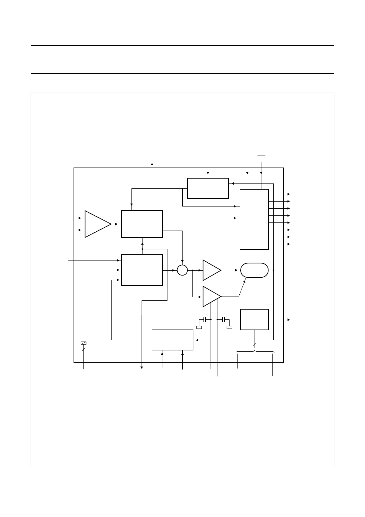
BLOCK DIAGRAM
andbook, full pagewidth
DIN
DINQ
33
34
LOS
39
ALEXANDER
PHASE
DETECTOR
enable
SEL155
30
FREQUENCY
DIVIDER 1
4/16
TZA3004HL
AREF
DATA
AND
CLOCK
OUTPUT
TZA3004HL
ENL
1
48
42
DOUT
43
DOUTQ
45
COUT
46
COUTQ
6
DLOOP
7
DLOOPQ
3
CLOOP
4
CLOOPQ
CREF
CREFQ
21
22
17
2, 5, 8, 10, 11, 14, 17,
20, 23, 26, 29, 32, 35,
38, 41, 44, 47
GND
FREQUENCY
WINDOW
DETECTOR
(1000 ppm)
FREQUENCY
12 24 25
DREF19LOCK
DIVIDER 2
64/128
9
+
∫
dt
CAPDOQDREF39
CAPUPQ
proportional
path
integrating
path
130 pF130 pF
1516
V
EE1
VCRO
POWER
CONTROL
4
27
V
EE3
V
EE2
37
PC
28
31
MGU255
V
EE4
Fig.1 Block diagram.
2000 Nov 28 3
Page 4

Philips Semiconductors Product specification
SDH/SONET data and clock recovery unit
STM1/4 OC3/12
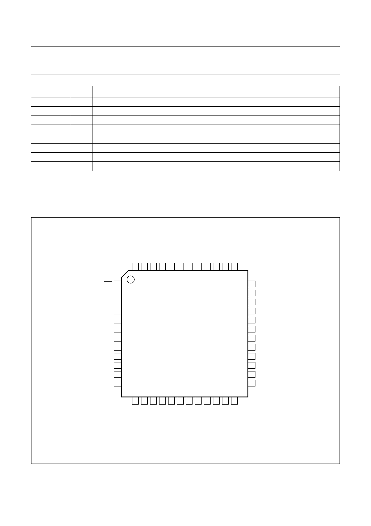
PINNING
SYMBOL PIN DESCRIPTION
ENL 1 loop mode enable input (active LOW)
GND 2 ground; note 1
CLOOP 3 clock output in loop mode (differential)
CLOOPQ 4 inverted clock output in loop mode (differential)
GND 5 ground; note 1
DLOOP 6 data output in loop mode (differential)
DLOOPQ 7 inverted data output in loop mode (differential)
GND 8 ground; note 1
DREF19 9 reference frequency select input 1 (see Table 3)
GND 10 ground; note 1
GND 11 ground; note 1
LOCK 12 phase lock detection output
i.c. 13 internally connected; note 2
GND 14 ground; note 1
CAPUPQ 15 external loop filter capacitor connection
CAPDOQ 16 external loop filter capacitor return connection
GND 17 ground; note 1
i.c. 18 internally connected; note 2
i.c. 19 internally connected; note 2
GND 20 ground; note 1
CREF 21 reference clock input (differential)
CREFQ 22 inverting reference clock input (differential)
GND 23 ground; note 1
DREF39 24 reference frequency select input 2 (see Table 3)
V
EE1
GND 26 ground; note 1
V
EE2
V
EE3
GND 29 ground; note 1
SEL155 30 STM mode select input 3 (see Table 2)
V
EE4
GND 32 ground; note 1
DIN 33 data input (differential)
DINQ 34 inverting data input (differential)
GND 35 ground; note 1
i.c. 36 internally connected; note 2
PC 37 control output for negative power supply
GND 38 ground; note 1
LOS 39 loss of signal detection output
i.c. 40 internally connected; note 2
25 negative supply voltage (−3.3 V); note 3
27 negative supply voltage (−3.3 V); note 3
28 negative supply voltage (−3.3 V); note 3
31 negative supply voltage (−3.3 V); note 3
TZA3004HL
2000 Nov 28 4
Page 5
Philips Semiconductors Product specification
SDH/SONET data and clock recovery unit
TZA3004HL
STM1/4 OC3/12
SYMBOL PIN DESCRIPTION
GND 41 ground; note 1
DOUT 42 data output in normal mode (differential)
DOUTQ 43 inverted data output in normal mode (differential)
GND 44 ground; note 1
COUT 45 clock output in normal mode (differential)
COUTQ 46 inverted clock output in normal mode (differential)
GND 47 ground; note 1
AREF 48 reference voltage input for controlling voltage swing on data and clock outputs
Notes
1. ALL GND pins must be connected; do not leave one single GND pin unconnected.
2. ALL pins denoted ‘i.c.’ have internal connections; external connections to these pins should not be made.
3. ALL VEE pins must be connected; do not leave one single VEE pin unconnected.
handbook, full pagewidth
ENL
GND
CLOOP
CLOOPQ
GND
DLOOP
DLOOPQ
GND
DREF19
GND
GND
LOCK
COUTQ
GND
47
14
GND
COUT
46
45
15
16
CAPUPQ
CAPDOQ
GND
44
TZA3004HL
17
GND
AREF
48
1
2
3
4
5
6
7
8
9
10
11
12
13
i.c.
DOUT
DOUTQ
43
42
18
19
i.c.
i.c.
GND
41
20
GND
i.c.
40
21
CREF
GND
LOS
39
38
22
23
GND
CREFQ
PC
24 37
DREF39
36
35
34
33
32
31
30
29
28
27
26
25
MGU254
i.c.
GND
DINQ
DIN
GND
V
EE4
SEL155
GND
V
EE3
V
EE2
GND
V
EE1
Fig.2 Pin configuration.
2000 Nov 28 5
Page 6

Philips Semiconductors Product specification
SDH/SONET data and clock recovery unit
STM1/4 OC3/12
FUNCTIONAL DESCRIPTION
The TZA3004HL recovers data and clock signals from an
incoming high speed bitstream. The input signal on
pins DIN and DINQ is buffered and amplified by the input
circuitry (see Fig.1). The signal is then fed into the
Alexander phase detector where the phase of the
incoming data signal is compared with that of the internal
clock. If the signals are out of phase, the phase detector
generates correction pulses (up or down) that shift the
phase of the Voltage Controlled Ring Oscillator (VCRO)
output in discrete amounts (∆ϕ) until the clock and data
signals are in phase. The technique used is based on
principles first proposed by J. D. H. Alexander, hence the
name of the phase detector.
Data sampling
As shown in Fig.3, the eye pattern of the incoming data is
sampled at three instants A, T and B. When clock and
data signals are synchronized (locked):
• A is the centre of the data bit
• T is in the vicinity of the next transition
• B is in the centre of the bit following the transition.
If the same level is recorded at both A and B, a transition
has not occurred and no action is taken. However, if the
levels at A and B are different, a transition has occurred
and the phase detector uses the level at T to determine
whether the clock was too early or too late with respect to
the data transition.
If the levels at A and T are the same but are different from
the level at B, the clock was too early and needs to be
slowed down a little. The Alexander phase detector then
generates a down pulse which stretches a single output
pulse from the ring oscillator by approximately 0.25%
which is 4 ps of the 1.6 ns bit period in the STM4/OC12
mode. This forces the VCRO to run at a slightly lower
frequency for one bit period. The phase of the clock signal
is thus shifted fractionally with respect to the data signal.
TZA3004HL
If the levels at B and T are the same but are different from
the level at A, the clock was too late and needs to be
speeded up for synchronization. The phase detector
generatesanuppulseforcingthe VCRO to run at a slightly
higherfrequency(+0.25%)foronebitperiod.Thephaseof
theclocksignalisshiftedwithrespecttothedatasignal(as
above, but in the opposite direction). While making these
phase adjustments, only the proportional path is active.
This type of loop is known as a Bang/Bang Phase-Locked
Loop (PLL) as the instantaneous frequency of the VCRO
changes in one of two discrete steps (±0.25%).
If the phase and the frequency of the VCRO are incorrect,
a long train of up or down pulses is generated. This train of
pulses is integrated to generate a control voltage that is
used to shift the centre frequency of the VCRO. Once the
correct frequency has been established, only the phase
will need to be adjusted for synchronization. The
proportional path adjusts the phase of the clock signal,
whereas the integrating path adjusts the centre frequency.
Frequency window detector
The frequency window detector checks the VCRO
frequency which has to be within a 1000 ppm (parts per
million) window around the required frequency.
It compares the output of frequency divider 2 with the
reference frequency on pins CREF and CREFQ
(19.44 or 38.88 MHz;see Table 3). IftheVCRO frequency
is found to be outside this window, the frequency window
detectordisablestheAlexander phase detector and forces
the VCRO output to a frequency within the window. The
phase detector then starts acquiring lock again. Due to the
loosecoupling of 1000 ppm,thereferencefrequencydoes
notneed to be highly accurate or stable.Any crystal based
oscillator that generates a reasonably accurate frequency
(e.g. 100 ppm) can be used.
Since sampling point A is always in the centre of the eye
pattern when the data and clock signals are in phase
(locked), the values recorded at this point are taken as the
retrieved data. The data and clock signals are available at
the CML output buffers, that are capable of driving a 50 Ω
load.
handbook, halfpage
DATADATA
ATB
CLOCK
MGK143
Fig.3 Data sampling.
2000 Nov 28 6
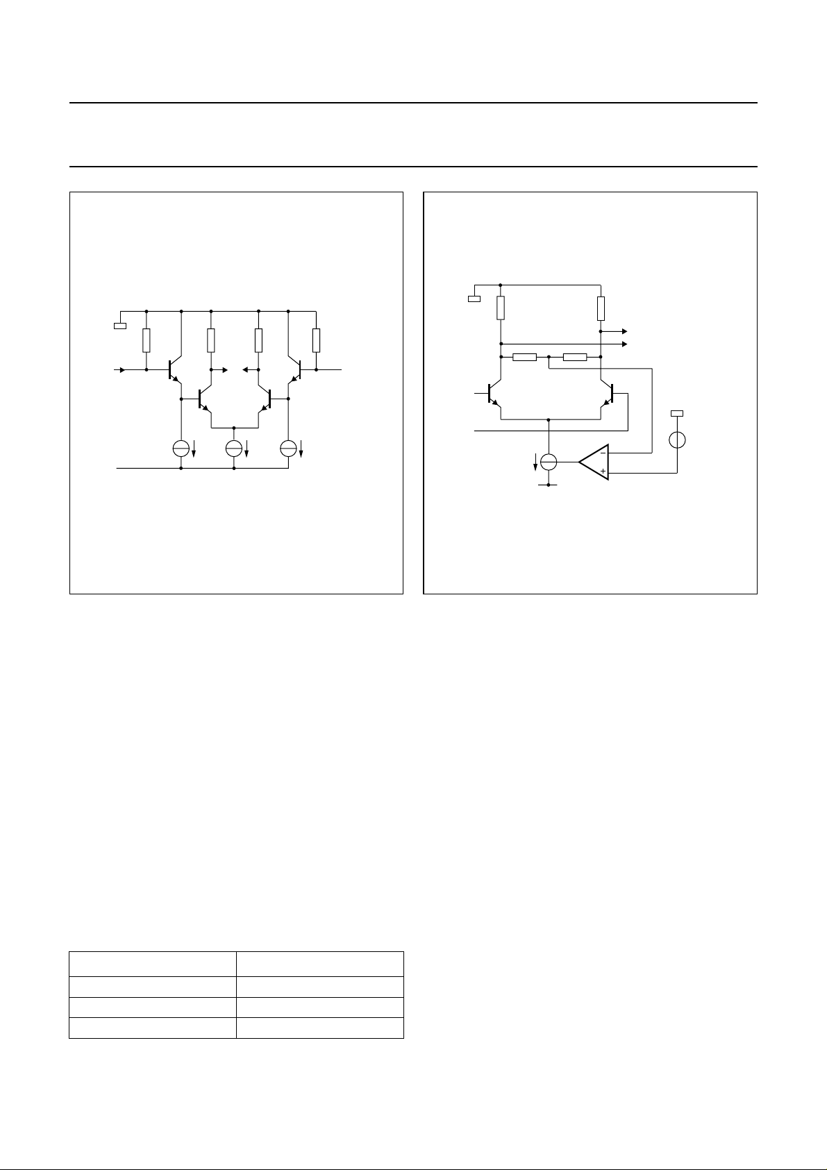
RF data and clock input circuit
The schematic of the input circuit is shown in Fig.4.
RF data and clock output circuit
The schematic of the output circuit is shown in Fig.5.
Page 7
Philips Semiconductors Product specification
SDH/SONET data and clock recovery unit
STM1/4 OC3/12
handbook, halfpage
50 Ω50 Ω
MGL669
DINQ,
CREFQ
DIN,
CREF
VEE
TZA3004HL
100 Ω100 Ω
DOUTQ, COUTQ
DOUT, COUT
V
AREF
V
EE
MGL670
Fig.4 RF data and clock input circuit.
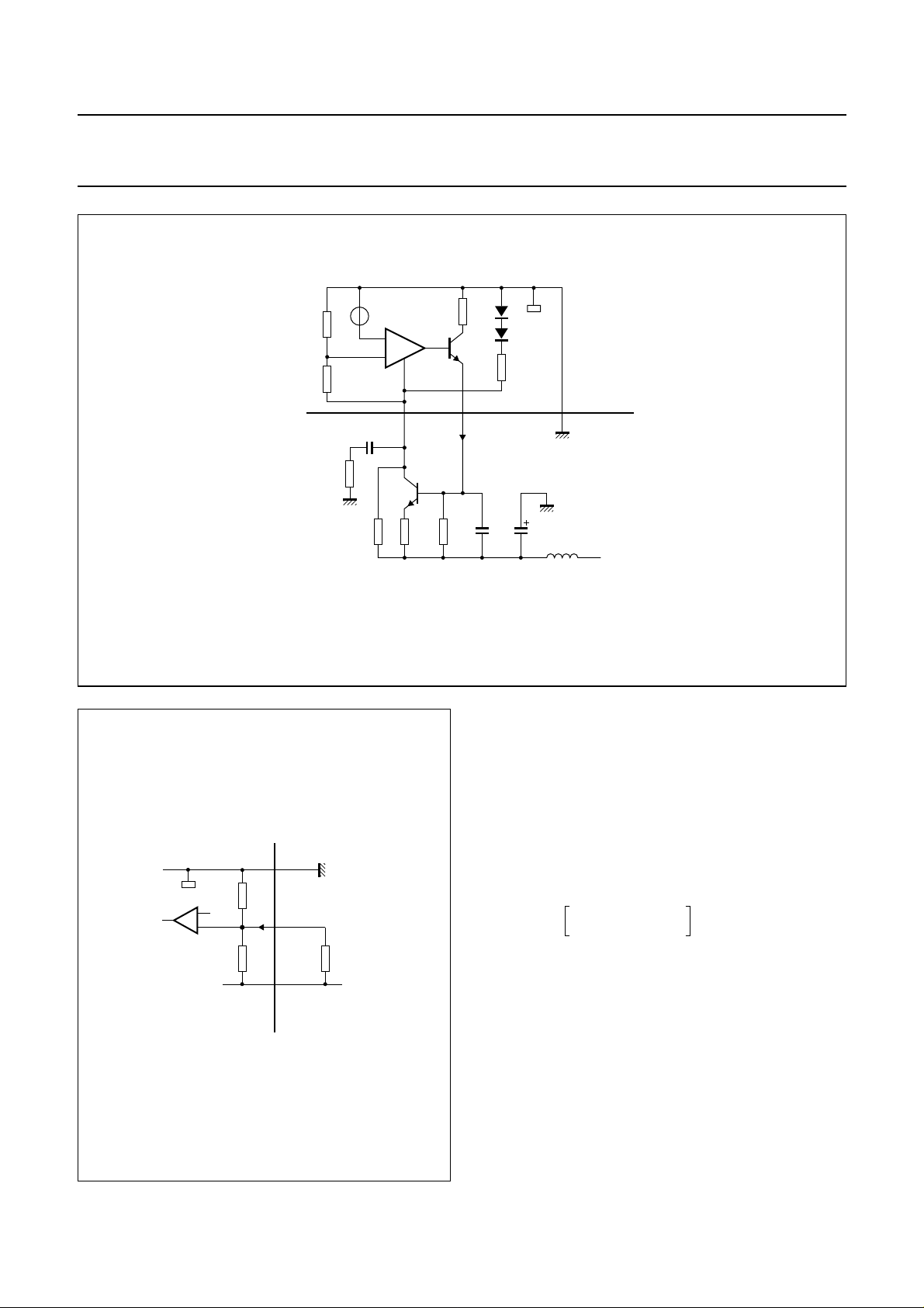
Power supply and power control loop
The TZA3004HL contains an on-board voltage regulator.
An external power transistor is needed to deliver the
supply to this circuit. The external circuit requirement is
straightforward and needs few components. A suitable
circuit with a power supply of −4.5 V is illustrated in Fig.6.
The inductor shown is an RF choke with an impedance
greater than 50 Ω at frequencies higher than 2 MHz. Any
transistor with a β of approximately 100 and enough
current sink capability can be used.
The TZA3004HL can also be used with a power supply of
−5.0 or −5.2 V. The only adaptation to be made to the
power control circuit is to change the emitter resistor R1
(see Fig.6 and Table 1).
As long as the power supply rejection ratio is greater than
60 dB for all frequencies, a different power supply
configuration could be used.
Table 1 Value of resistor R1.
POWER SUPPLY RESISTOR R1
−4.5 V 2.0 Ω
−5.0 V 6.8 Ω
−5.2 V 8.2 Ω
Fig.5 RF data and clock output circuit.
Output amplitude reference
The voltage swing at the CML-compatible output stages
(pins DOUT, DOUTQ, COUT, COUTQ, DLOOP,
DLOOPQ, CLOOP and CLOOPQ) can be controlled by
adjusting the voltage on pin AREF (see Fig.7). An internal
voltage divider of 500 Ω and 16 kΩ connected between
ground and VEE initially fixes this level.
In most applications the outputs will be DC-coupled to
a load of 50 Ω. The output level regulation circuit will
maintain a 200 mV (p-p) single-ended swing across this
load. The voltage on pin AREF is half the single-ended
peak-to-peak value of the output signal (−100 mV).
No adjustments are necessary with DC-coupling.
When the outputs are AC-coupled, the voltage on
pin AREF is half the single-ended peak-to-peak value of
the output signal multiplied by a factor
RLRo+
-------------------R
L
where RL is the external load and Ro is the output
impedance of the TZA3004HL (100 Ω).
2000 Nov 28 7
Page 8
Philips Semiconductors Product specification
SDH/SONET data and clock recovery unit
STM1/4 OC3/12
handbook, full pagewidth
2 Ω
100 nF
1 kΩ
BAND GAP
REFERENCE
V
EE
β ≈ 100
R1
2 Ω
1
kΩ
PC
3.3
nF
GND
1 µF
TZA3004HL
on chip
off chip
(1)
L1
−4.5 V
MGU253
(1) L1 = RF choke type Murata BLM21, 1 µH.
Fig.6 Schematic diagram of TZA3004HL power control loop.
handbook, halfpage
500 Ω
16 kΩ R
GND
AREF
V
EE
If the outputs are AC-coupled, the formulae for calculating
the required voltage on pin AREF and the value of the
resistor connected between pins AREF and VEE are:
V
AREF
RLRo+
-------------------R
L
×–=
0.5V
swing
(1)
and:
V
EE
V
AREF
AREF
R1
×
---------------- -
V
AREF
=
------------------------------------------------------------1
R
AREF
R1
×–
------- -
R2
where R1 = 500 Ω, R2 = 16 kΩ and VEE= −3.3 V.
V
EE
---------------- V
AREF
1–
(2)
1–
To maintain a single-ended swing of 200 mV (p-p) across
a50ΩAC-coupled load, the voltage onpin AREF must be
off chipon chip
MGL667
100 mV–
50 + 100()Ω
× 300 mV.–=
---------------------------------
50 Ω
Fig.7 Functionality of pin AREF.
2000 Nov 28 8
This can be achieved by connecting a 7.3 kΩ resistor
between pins AREF and VEE.
Page 9
Philips Semiconductors Product specification
SDH/SONET data and clock recovery unit
STM1/4 OC3/12
External capacitor for loop filter
The loop filter is an integrator with a built-in capacitance of
2 × 130 pF. To ensure loop stability while the frequency
window detector is active, an external capacitance of
200 nF should be connected between pins CAPUPQ
and CAPDOQ.
Loop mode enable
The loop mode is provided for system testing (see Fig.8).
Loop mode is enabled by applying a voltage lower than
0.8 V (TTL LOW-level) to pin ENL. In loop mode, the
outputs on pins DLOOP, DLOOPQ, CLOOP and
CLOOPQ are switched on.
A voltage higher than 2.0 V (TTL HIGH-level) applied to
pin ENL switches on pins DOUT, DOUTQ, COUT
and COUTQ while pins DLOOP, DLOOPQ, CLOOP
and CLOOPQ are disabled to minimize power
consumption.
Connecting pin ENL to VEE(−3.3 V) enables all outputs.
handbook, halfpage
off chip on chip
ENL
36 kΩ
GND
DECODER
LOGIC
V
EE
MGL668
TZA3004HL
Lock detection
The LOCK output can be interpreted as an indication that
the reference clock is present on pin CREF and that the
acquisition aid (frequency window detector) is functioning
properly.
LOCK is an open-collector TTL output to be connected via
a10kΩpull-up resistor to a positive supply voltage. If the
VCO frequency is within a 1000 ppm window around the
desired frequency, pin LOCK will stay at HIGH-level. If no
reference clock is present, or the VCO is outside the
1000 ppm window, pin LOCK will be at a LOW-level. The
logic level on pin LOCK does not indicate locking of the
PLL to the incoming data; this is done by the signal on
pin LOS.
Loss of signal detection
The Loss Of Signal (LOS) function is closely related to the
functionalityof the Alexander phase detector (see Fig.3 for
the meaning of A, B and T in this section).
The phase detector takes no action if there has been no
transition and the values at sample points A and B are the
same. However, if levels A and B are equal but level at T
is different, even with no transition, the incorrect level at T
could lead to a bit error. This incorrect level could be due
tonoiseor from poor signal integrity. The cumulative affect
of bit errors could cause the PLL to lose lock and the LOS
alarm to be asserted. The LOS alarm assert level is
approximately Bit Error Rate (BER) = 5 × 10⁻² and the
de-assert level is approximately BER = 1 × 10⁻³.
LOS detection functions correctly if the input signal is
larger than the input offset of the TZA3004HL. If the input
signal is smaller, it is masked by the input offset and
interpreted as consecutive bits of the same sign, thus
obstructingLOS detection. In practice, an optical front-end
device with a noise level larger than the specified offset of
the TZA3004HL will ensure proper LOS indication.
The LOS detection is BER related, but not dependent on
the data stream content or protocol. Therefore, an
SDH/SONET data stream is no prerequisite for a proper
LOS function. Since the LOS function of the TZA3004HL
isderived from digital signals, it is a good supplement to an
analog, amplitude based, LOS indication.
Fig.8 Input circuit of pin ENL.
2000 Nov 28 9
Pin LOS is an open-collector TTL compatible output. that
needs a pull-up resistor connected to a positive supply
voltage to function.
The LOS pin will be at a(TTL) HIGH-level if the data signal
is absent on pins DIN and DINQ or if BER > 5 × 10⁻²;
otherwise pin LOS will be at LOW-level if BER < 1 × 10⁻³.
Page 10
Philips Semiconductors Product specification
SDH/SONET data and clock recovery unit
STM1/4 OC3/12
STM mode selection
The VCRO has a very wide tuning range. However, the
performance of the TZA3004HL is optimized for
SDH/SONET bit rates.
Due to the nature of the PLL, the very wide tuning range is
a necessity for proper lock behaviour over the guaranteed
temperature range, aging and batch-to-batch spread.
Though it may seem that the TZA3004HL is capable of
recovering bit rates other than SDH/SONET (STM1/OC3
and STM4/OC12), lock behaviour cannot be guaranteed.
The required SDH/SONET bit rate is selected by
connecting pin SEL155 to the ground plane or to the
supply voltage VEE (see Table 2):
• For STM4/OC12 (622.08 Mbits/s) operation, pin
SEL155 is to be connected to ground (pin GND)
• For STM1/OC3 (155,52 Mbits/s) operation, pin SEL155
is to be connected to VEE.
The connection to VEEor ground carries a current of a few
milliamperes and should have low resistance and
inductance; short printed-circuit board tracks are
recommended. In some cases it may be necessary to add
a decoupling capacitor near the selection pin to provide
a clean return path for RF signals.
TZA3004HL
Reference frequency select
A reference clock signal of 19.44 or 38.88 MHz must be
connected to pins CREF and CREFQ. Pins DREF19
and DREF39 are used to select the appropriate output
frequency at frequency divider 2 (see Table 3).
To minimize the adverse influence of reference clock
crosstalk, a differential signal with an amplitude from
75 to 150 mV (p-p) is advised.
Sincethe reference clock is only used as an acquisition aid
for the PLL of the frequency window detector, the quality
of the reference clock (i.e. phase noise) is not important.
There is no phase noise specification imposed on the
reference clock generator and even frequency stability
may be in the order of 100 ppm. In general, most
inexpensive crystal-based oscillators are suitable.
There are two application possibilities for the TZA3004HL
reference clock:
• A fixed reference clock frequency, here it is best to
connect pins DREF19 and DREF39 using a short track
or a via to the ground plane or the supply voltage V
• Aselectable reference clock frequency in which the pins
can be controlled through low-ohmic switching FETs,
e.g. BSH103 or equivalent (low R
DSon
).
EE
Whenthe TZA3004HL is used in anapplicationwith a fixed
datarate it is best to connect pin SEL155 byashortcopper
trace or a via to the ground plane or supply voltage VEE.
If a selectable reference clock frequency is required in the
application, the pin can be controlled through a low-ohmic
switching FET, e.g. BSH103 or equivalent (low R
DSon
).
Table 2 STM mode select
MODE
BIT RATE
(Mbits/s)
STM1/OC3 155.52 16 V
DIVISION
FACTOR
LEVEL ON
PIN SEL155
EE
STM4/OC12 622.08 4 ground
Table 3 Reference frequency selection
FREQUENCY
(MHz)
DIVISION
FACTOR
LEVEL ON PIN
DREF19 DREF39
38.88 64 ground V
19.44 128 V
EE
EE
V
EE
2000 Nov 28 10
Page 11

Philips Semiconductors Product specification
SDH/SONET data and clock recovery unit
STM1/4 OC3/12
Application with positive supply voltage
The versatile design of the TZA3004HL allows the device
to operate in a positive supply voltage application,
although some pins then have a different operating mode.
This section deals with these differences and supports the
user with achieving a successful application of the
TZA3004HL in a +5 V environment.
APPLICATION DIAGRAM
A sample application diagram is shown in Fig.22. It should
be noted that all GND pins are now connected to VCCand
all VEEpins are still connected to the regulated voltage
from the power controller.
OUTPUT SELECTION
In a positive supply voltage application, the loop mode is
the default RF output. Due to the decoding logic on
pin ENL, it is only possible to select the loop mode outputs
or enable all the outputs.
If pin ENL is connected to VCC(+5 V), only the loop mode
outputs are active (see Table 4). When pin ENL is
connected to VEE (the voltage is approximately 3.3 V
below VCC), all outputs become active. In the positive
supply voltage application, the normal mode outputs
cannot be selected, unless the voltage on pin ENL is 2 V
above the positive supply voltage (VCC).
TZA3004HL
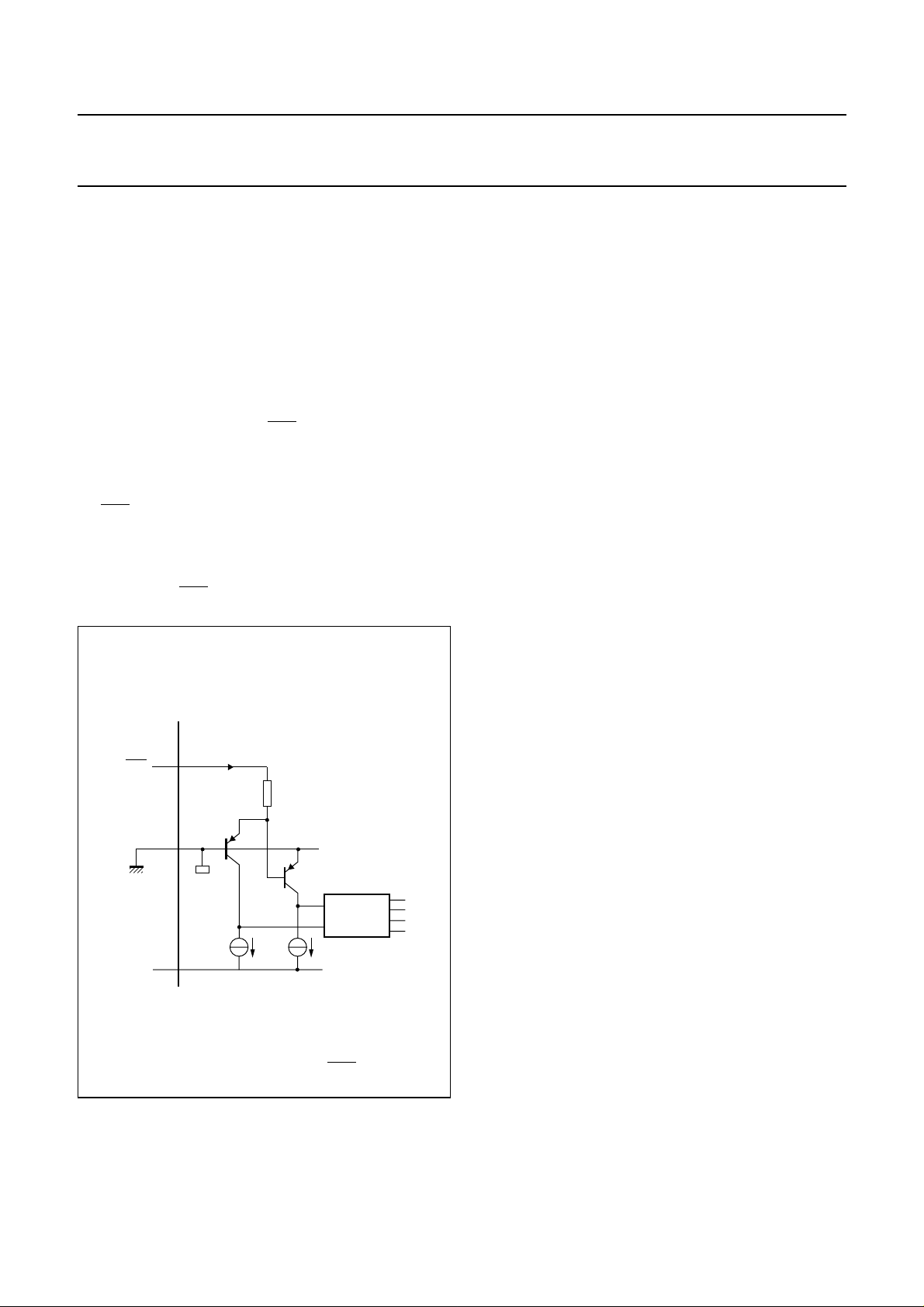
LOSS OF SIGNAL AND LOCK DETECTION
In the negative supply application, pins LOS and LOCK
are open-collector outputs that require pull-up resistors to
a positive supply voltage.
Inthe positive supply application, thepull-upvoltage would
need to be higher than the positive supply voltage. The
signals on pins LOS and LOCK would no longer be TTL
compatible. However, the internal circuit on pins LOS and
LOCK can be used in a current mirror configuration (see
Fig.9). This requires only an external PNP transistor (e.g.
BC857 or equivalent) to mirror the current. A 10 kΩ
pull-down resistor from the collector of the external
transistor to ground yields a TTL compatible signal again
but it is inverted. The meaning of the LOS and LOCK flag
when used in the positive supply application is shown in
Table 5.
handbook, halfpage
GND
LOS,
LOCK
off chipon chip
+5 V
BC857
signal out
10 kΩ
MGL671
a positive supply voltage application.
Do not to connect pin
destroy the IC.
CAUTION
ENL to ground, because this will
Fig.9 Signaloutput for LOS andLOCKindication in
Table 4 Output selection in a positive supply voltage application
OUTPUT
MODE LEVEL ON PIN ENL
Loop V
Loop and normal V
Normal V
CC
(VCC− 3.3 V) active active
EE
CC
(+5 V) active −
+2V − active
DLOOP, DLOOPQ,
CLOOPAND CLOOPQ
DOUT, DOUTQ,
COUTAND COUTQ
Table 5 LOS and LOCK indication in a positive supply voltage application
SIGNAL DESCRIPTION LEVEL TTL
LOS active loss of signal: BER > 5 × 10
−2
LOS inactive no loss of signal: BER < 1 × 10
−3
0 V (ground) LOW
+5 V (VCC) HIGH
LOCK active reference clock present and VCRO inside 1000 ppm window 0 V (ground) LOW
LOCK inactive no reference clock present or VCRO outside 1000 ppm window +5 V (V
) HIGH
CC
2000 Nov 28 11
Page 12

Philips Semiconductors Product specification
SDH/SONET data and clock recovery unit
STM1/4 OC3/12
DIVIDER SETTINGS
The reference frequency dividers and the STM mode
selectors operate in a similar manner in a positive supply
voltage application. The only difference is that pins
formerly connected to ground should now be connected to
VCC (+5 V). Pins connected to VEE should continue to be
connected to VEE, as connecting these pins to ground
(0 V) will damage the IC.
RF INPUT AND OUTPUTS
All RF inputs, outputs and internal signals of the
TZA3004HL are referenced to pins GND. In the positive
supply voltage application, this means that all RF signals
are referenced to VCC. Therefore a clean VCC rail is of
ultimate importance for proper RF performance. The best
performance is obtained when the transmission line
reference plane is also decoupled to VCC. Careful design
ofVCCandgood decoupling schemes should be taken into
account. While designing the printed-circuit board, keep in
mind that the VCChas become what was formerly ground.
TZA3004HL
Whilelaying out the application, the return pathis the most
important issue to be considered. Always examine
carefully the current-carrying loops in the design. Care
should be taken that low-ohmic and low-inductance return
paths are available for all frequencies (both of interest and
not of interest). These return paths should preferably have
an enclosed area as small as possible, both horizontally
and vertically (by means of through-holes or vias). The
position of a decoupling capacitor is very important.
A decoupling capacitor in an unfavourable position could
do more damage than would completely omitting the
capacitor. In the correct location it could be the difference
between mediocre results and the ultimate achievement.
2000 Nov 28 12
Page 13

Philips Semiconductors Product specification
SDH/SONET data and clock recovery unit
TZA3004HL
STM1/4 OC3/12
LIMITING VALUES
In accordance with the Absolute Maximum Rating System (IEC 60134).
SYMBOL PARAMETER MIN. MAX. UNIT
V
EE
V
n
I
n
P
tot
T
amb
T
j
T
stg
negative supply voltage −6 +0.5 V
DC voltage on pins
CLOOP, CLOOPQ, DLOOP, DLOOPQ, CREF, CREFQ, DIN, DINQ,
−1 +0.5 V
DOUT, DOUTQ, COUT and COUTQ
ENL, LOCK and LOS, VEE− 0.5 +5.5 V
DREF19, DREF39, SEL155, PC and AREF V
CAPUPQ and CAPDOQ V
− 0.5 +0.5 V
EE
+ 0.5 −0.5 V
EE
input current on pins
ENL − 1mA
CREF, CREFQ, DIN and DINQ −20 +10 mA
total power dissipation − 700 mW
ambient temperature −40 +85 °C
junction temperature − +110 °C
storage temperature −65 +150 °C
HANDLING INSTRUCTIONS
Precautions should be taken to avoid damage through electrostatic discharge.
THERMAL CHARACTERISTICS
SYMBOL PARAMETER CONDITIONS VALUE UNIT
R
R
th(j-s)
th(j-a)
thermal resistance from junction to solder point 46 K/W
thermal resistance from junction to ambient in free air; note 1 67 K/W
Note
1. Thermal resistance from junction to ambient is determined with the IC soldered on a standard single sided
57 × 57 × 1.6 mm FR4 epoxy PCB with 35 µm thick copper traces. The measurements are performed in still air.
2000 Nov 28 13
Page 14

Philips Semiconductors Product specification
SDH/SONET data and clock recovery unit
TZA3004HL
STM1/4 OC3/12
CHARACTERISTICS
VEE= −3.3 V; T
to GND; unless otherwise specified.
SYMBOL PARAMETER CONDITIONS MIN. TYP. MAX. UNIT
Supplies
V
EE
I
EE
P
tot
Data and clock inputs: pins DIN, DINQ, CREF and CREFQ
V
i(p-p)
V
i(sens)(p-p)
V
IO
V
I
Z
i
Data and clock outputs: pins DOUT, DOUTQ, DLOOP, DLOOPQ, COUT, COUTQ, CLOOP and CLOOPQ
V
o(p-p)
V
O
Z
o
t
r(C)
t
f(C)
t
r(D)
t
f(D)
t
d(D-C)
Output amplitude adjustment: pin AREF
V
AREF
Power control output: pin PC
g
m
I
O
Loop mode enable input: pin ENL
V
IL
V
IH
Phase lock indicator: pin LOCK
V
OL
V
OH
= −40 to +85 °C; typical values measured at T
amb
=25°C; all voltages are measured with respect
amb
negative supply voltage see Fig.12; note 1 −3.50 −3.30 −3.10 V
negative supply current open outputs; see Fig.13 − 112 155 mA
total power dissipation − 370 550 mW
input voltage
(peak-to-peak value)
input sensitivity
(peak-to-peak value)
50 Ω measurement system;
see Fig.10; notes 2 and 3
50 Ω measurement system;
notes 2 and 4
7 200 450 mV
− 2.5 7 mV
DC input offset voltage 50 Ω measurement system −3 0 +3 mV
input voltage 50 Ω measurement system −600 −200 +250 mV
input impedance single-ended; see Fig.4; note 5 − 50 −Ω
output voltage swing
(peak-to-peak value)
50 Ω measurement system;
single-ended; see Fig.10
default adjustment; note 6 170 200 210 mV
special adjustment; note 7 50 − 400 mV
output voltage −600 − 0mV
output impedance single-ended − 100 −Ω
clock output rise time differential; 20% to 80% − 90 − ps
clock output fall time differential; 20% to 80% − 90 − ps
data output rise time differential; 20% to 80% − 200 − ps
data output fall time differential; 20% to 80% − 200 − ps
data-to-clock delay see Fig.11; note 8 250 280 310 ps
output amplitude reference
floating pin −110 −100 −90 mV
voltage
transconductance −84 −60 −42 mA/V
output current 1 − 3.5 mA
LOW-level input voltage −− 0.8 V
HIGH-level input voltage 2.0 −−V
LOW-level output voltage note 9 −0.6 −−V
HIGH-level output voltage note 9 −− 3.3 V
2000 Nov 28 14
Page 15

Philips Semiconductors Product specification
SDH/SONET data and clock recovery unit
TZA3004HL
STM1/4 OC3/12
SYMBOL PARAMETER CONDITIONS MIN. TYP. MAX. UNIT
Loss of signal indicator: pin LOS
V
OL
V
OH
t
as
t
das
BER
as
BER
das
PLL characteristics
t
acq
J
tol(p-p)
J
gen(p-p)
J
gen(rms)
TDR transitionless data run note 13 − 2000 − bits
LOW-level output voltage note 9 −0.6 −−V
HIGH-level output voltage note 9 −− 3.3 V
assert time note 10 − 0.1 −µs
de-assert time note 10 − 10 −µs
assert bit error rate note10 − 5 × 10⁻²− BER
de-assert bit error rate note 10 − 1 × 10⁻³− BER
acquisition time CREF = 19.44 MHz − 100 200 µs
CREF = 38.88 MHz − 50 200 µs
jitter tolerance
(peak-to-peak value)
STM1/OC3 mode; note 11
f = 6.5 kHz 1.5 >10 − UI
f = 65 kHz 0.15 1.3 − UI
f = 1 MHz 0.15 0.8 − UI
STM4/OC12 mode; note 11
f = 25 kHz 1.5 >10 − UI
f = 250 kHz 0.15 1.3 − UI
f = 5 MHz 0.15 0.35 − UI
jitter generation
(peak-to-peak value)
STM1/OC3 mode; note 12
f = 500 Hz to 1.3 MHz − 0.039 0.50 UI
f = 12 kHz to 1.3 MHz − 0.032 0.10 UI
f = 65 kHz to 1.3 MHz − 0.032 0.10 UI
STM4/OC12 mode; note 12
f = 1 kHz to 5 MHz − 0.050 0.50 UI
f = 12 kHz to 5 MHz − 0.040 0.10 UI
f = 250 kHz to 5 MHz − 0.052 0.10 UI
jitter generation (RMS value) STM1/OC3 mode; note 12
f = 500 Hz to 1.3 MHz − 0.0060 − UI
f = 12 kHz to 1.3 MHz − 0.0046 − UI
f = 65 kHz to 1.3 MHz − 0.0041 − UI
STM4/OC12 mode; note 12
f = 1 kHz to 5 MHz − 0.0093 − UI
f = 12 kHz to 5 MHz − 0.0079 − UI
f = 250 kHz to 5 MHz − 0.0081 − UI
2000 Nov 28 15
Page 16

Philips Semiconductors Product specification
SDH/SONET data and clock recovery unit
TZA3004HL
STM1/4 OC3/12
Notes to the characteristics
1. Typical power supply voltage for the voltage regulator is −4.5 V (see Fig.6).
2. It is assumed that both CML inputs carry a complementary signal with the specified peak-to-peak value (true
differential excitation).
3. The specified input voltage range is the guaranteed and tested range for proper operation; BER < 1 × 10
4. An input sensitivity of 7 mV (p-p) for BER < 1 ⋅ 10
is 2.5 mV (p-p).
5. CML inputs are terminated internally using on-chip resistors of 50 Ω connected to ground.
6. Output voltage range with default reference voltage on pin AREF (floating).
7. Output voltage range with adjustment of voltage on pin AREF (see Section “Output amplitude reference”).
8. Measured with 1010 data pattern, single-ended output signals and rising edges of the signals on
pins COUT to DOUT or pins CLOOP to DLOOP. It should be noted that small deviations of the specified value are
possible if measured differentially.
9. External pull-up resistor of 10 kΩ connected to supply voltage of +3.3 V.
10. LOS assert or de-assert timing and BER level are for indication only. The values are neither production tested nor
guaranteed.
11. Measured in accordance with ITU specification G.958. Measured on demoboard OM5802 for STM1/OC3 and
STM4/OC12. For more information, see
12. Measured in accordance with ITU specification G.813 and 1 dB above the system input sensitivity power level.
Measured on demoboard OM5802 for STM1/OC3 and STM4/OC12.
13. TDR is bit rate independent.
“Application note AN97065”
−10
is guaranteed. The typical input sensitivity for BER < 1 × 10
.
−10
.
−10
2000 Nov 28 16
Page 17

Philips Semiconductors Product specification
SDH/SONET data and clock recovery unit
STM1/4 OC3/12
handbook, full pagewidth
V
I(max)
V
IQH
V
IH
V
IQL
V
IL
V
I(min)
CML INPUT
V
IO
GND
V
i(p-p)
V
O(max)
V
V
V
O(min)
OQH
V
OH
OQL
V
OL
CML OUTPUT
V
OO
TZA3004HL
GND
V
o(p-p)
MGK144
handbook, full pagewidth
COUT or
CLOOP
DOUT or
DLOOP
Fig.10 Logic level symbol definitions for CML.
t
d(D-C)
MGL672
GND
−200 mV
GND
−200 mV
Fig.11 Data-to-clock delay for CML outputs: COUT to DOUT or CLOOP to DLOOP.
2000 Nov 28 17
Page 18

Philips Semiconductors Product specification
SDH/SONET data and clock recovery unit
STM1/4 OC3/12
TYPICAL PERFORMANCE CHARACTERISTICS
−3.30
handbook, halfpage
V
EE
(V)
−3.35
−3.40
−3.45
−40
It should be noted that the voltage on pins VEE is regulated by the
power controller.
0 40 12080
MGL650
T (°C)
160
handbook, halfpage
I
EE
(mA)
120
80
40
0
−40 0 40 120
TZA3004HL
MGU252
80
T (°C)
Fig.12 Supply voltage as a function of the
temperature.
Fig.13 Supply current as a function of the
temperature.
2000 Nov 28 18
Page 19

Philips Semiconductors Product specification
SDH/SONET data and clock recovery unit
STM1/4 OC3/12
MGL658
BER
10
10
10
10
1
−1
−2
−3
−4
handbook, halfpage
BER
10
10
10
10
1
−1
−2
−3
−4
handbook, halfpage
TZA3004HL
MGL657
−5
10
−6
10
−7
10
−8
10
−9
10
−10
10
−11
10
V
i(p-p)
(mV)
1.50.5 10
−5
10
−6
10
−7
10
−8
10
−9
10
−10
10
−11
10
V
i(p-p)
(mV)
1.50.5 10
A complementary input signal of the indicated
value is applied to pins DIN and DINQ.
Fig.14 Bit error rate as a function of the input signal
in STM1/OC3 mode (155.52 Mbits/s).
2000 Nov 28 19
A complementary input signal of the indicated
value is applied to pins DIN and DINQ.
Fig.15 Bit error rate as a function of the input signal
in STM4/OC12 mode (622.08 Mbits/s).
Page 20

Philips Semiconductors Product specification
SDH/SONET data and clock recovery unit
STM1/4 OC3/12
3
10
handbook, full pagewidth
J
tol(p-p)
(UI)
2
10
10
1
−1
10
1
10
10
TZA3004HL
MGL659
(1)
(2)
2
3
10
f (kHz)
4
10
(1) Device performance measured on OM5802 demoboard.
(2) ITU specification template.
Fig.16 Jitter tolerance as a function of the jitter frequency in the STM1/OC3 mode (155.52 Mbits/s).
3
J
tol(p-p)
(UI)
10
2
10
10
1
(1)
(2)
handbook, full pagewidth
MGL660
−1
10
1
(1) Device performance measured on OM5802 demoboard.
(2) ITU specification template.
10 10
Fig.17 Jitter tolerance as a function of the jitter frequency in the STM4/OC12 mode (622.08 Mbits/s).
2000 Nov 28 20
2
3
10
f (kHz)
4
10
Page 21

Philips Semiconductors Product specification
SDH/SONET data and clock recovery unit
STM1/4 OC3/12
handbook, full pagewidth
200 mV/div
TZA3004HL
MGS228
Measured single-ended.
handbook, full pagewidth
Fig.18 Data and clock output waveforms in the STM4/OC12 mode (622.08 Mbits/s).
MGT219
Measured differentially.
Fig.19 Clock output waveform in the STM4/OC12 mode (622.08 Mbits/s).
2000 Nov 28 21
Page 22

Philips Semiconductors Product specification
SDH/SONET data and clock recovery unit
STM1/4 OC3/12
handbook, full pagewidth
TZA3004HL
MGT220
Measured differentially.Measured differentially; PRBS 223− 1 pattern.
Fig.20 Data output waveform in the STM4/OC12 mode (622.08 Mbits/s).
2000 Nov 28 22
Page 23

Philips Semiconductors Product specification
SDH/SONET data and clock recovery unit
STM1/4 OC3/12
APPLICATION INFORMATION
handbook, full pagewidth
100 nF 100 nF
PRE-
AMP
38.88/19.44 MHz
system clock
V
EE
CAPUPQ
CAPDOQ
CREFQ
DREF19
DREF39
DIN
DINQ
CREF
15
16
33
34
TZA3004HL
21
22
9
24
2725
(1)
V
GND
17
EE1
V
EE2
28 31
V
EE3VEE4
37
39
12
42
43
45
46
48
30
PC
LOS
LOCK
DOUT
DOUTQ
COUT
COUTQ
DLOOP
6
DLOOPQ
7
CLOOP
3
CLOOPQ
4
ENL
1
AREF
SEL155
+3.3 V
+3.3 V
10 kΩ
10 kΩ
TZA3004HL
normal
output
loop
output
output
select
100
nF
2 Ω
(1) All pins GND must be connected directly to the PCB ground plane (pins 2, 5, 8, 10, 11, 14, 17, 20, 23, 26, 29, 32, 35, 38, 41, 44 and 47).
(2) L1 = RF choke type Murata BLM21.
kΩ
β ≈ 100
1
2 Ω
kΩ
1
3.3
nF
1 µF
1 µH
−4.5 V
MGU257
Fig.21 Application diagram showing the TZA3004HL configured for the STM4/OC12 mode (622.08 Mbits/s).
2000 Nov 28 23
Page 24

Philips Semiconductors Product specification
SDH/SONET data and clock recovery unit
STM1/4 OC3/12
handbook, full pagewidth
CAPUPQ
100 nF 100 nF
CAPDOQ
PRE-
AMP
39 MHz
system clock
CREFQ
DREF19
V
CC
DREF39
DIN
DINQ
CREF
i.c.
15
16
33
34
21
22
9
24
5
GND
13, 18, 19,
36, 40
(1)
TZA3004HL
V
V
EE1
EE2
28 31
V
EE3VEE4
372725
39
12
42
43
45
46
6
7
3
4
1
48
30
PC
LOS
LOCK
DOUT
DOUTQ
COUT
COUTQ
DLOOP
DLOOPQ
CLOOP
CLOOPQ
ENL
AREF
SEL155
TZA3004HL
V
CC
LOS
10 kΩ
V
CC
normal
output
loop
output
output
select
V
CC
10 kΩ
=
=
LOCK
unused
output
main
output
(3)
17
100
nF
2 Ω
V
V
CC
CC
(1) (1) All pins GND must be connected directly to VCCon the PCB plane of +5 V (pins 2, 5, 8, 10, 11, 14, 17, 20, 23, 26, 29, 32, 35, 38, 41, 44 and 47).
(2) L1 = RF choke type Murata BLM201, 1 µH.
(3) The loop mode outputs are used as main outputs:
pin ENL = HIGH-level selects loop mode outputs
pin ENL = LOW-level selects loop mode and normal mode outputs simultaneously.
kΩ
β ≈100
V
CC
1
2 Ω
kΩ
1
3.3
nF
1 µF
L1
(2)
MGU256
Fig.22 Application diagram showing the TZA3004HL configured for the STM4/OC12 mode (622.08 Mbits/s) with
a positive supply voltage application.
2000 Nov 28 24
Page 25

Philips Semiconductors Product specification
SDH/SONET data and clock recovery unit
STM1/4 OC3/12
PACKAGE OUTLINE
LQFP48: plastic low profile quad flat package; 48 leads; body 7 x 7 x 1.4 mm
c
y
X
36
37
25
Z
24
E
A
TZA3004HL
SOT313-2
e
w M
pin 1 index
48
1
e
DIMENSIONS (mm are the original dimensions)
mm
A
A1A2A3bpcE
max.
0.20
0.05
1.45
1.35
1.60
UNIT
Note
1. Plastic or metal protrusions of 0.25 mm maximum per side are not included.
b
p
0.25
w M
D
H
D
0.27
0.17
12
Z
D
(1) (1)(1)
D
0.18
7.1
0.12
6.9
b
p
13
v M
B
v M
0 2.5 5 mm
scale
(1)
eH
H
D
7.1
6.9
0.5
9.15
8.85
E
A
B
9.15
8.85
H
E
LL
E
0.75
0.45
A
p
A
2
A
1
L
detail X
Z
D
0.12 0.10.21.0
0.95
0.55
(A )
3
L
p
Zywv θ
E
0.95
0.55
θ
o
7
o
0
OUTLINE
VERSION
SOT313-2 MS-026136E05
IEC JEDEC EIAJ
REFERENCES
2000 Nov 28 25
EUROPEAN
PROJECTION
ISSUE DATE
99-12-27
00-01-19
Page 26

Philips Semiconductors Product specification
SDH/SONET data and clock recovery unit
STM1/4 OC3/12
SOLDERING
Introduction to soldering surface mount packages
Thistext gives a very brief insight to a complex technology.
A more in-depth account of soldering ICs can be found in
our
“Data Handbook IC26; Integrated Circuit Packages”
(document order number 9398 652 90011).
There is no soldering method that is ideal for all surface
mount IC packages. Wave soldering can still be used for
certainsurface mount ICs, but it is not suitableforfinepitch
SMDs. In these situations reflow soldering is
recommended.
Reflow soldering
Reflow soldering requires solder paste (a suspension of
fine solder particles, flux and binding agent) to be applied
totheprinted-circuitboardbyscreen printing, stencilling or
pressure-syringe dispensing before package placement.
Several methods exist for reflowing; for example,
convection or convection/infrared heating in a conveyor
type oven. Throughput times (preheating, soldering and
cooling) vary between 100 and 200 seconds depending
on heating method.
Typical reflow peak temperatures range from
215 to 250 °C. The top-surface temperature of the
packages should preferable be kept below 220 °C for
thick/large packages, and below 235 °C for small/thin
packages.
Wave soldering
Conventional single wave soldering is not recommended
forsurface mount devices (SMDs) or printed-circuit boards
with a high component density, as solder bridging and
non-wetting can present major problems.
To overcome these problems the double-wave soldering
method was specifically developed.
TZA3004HL
If wave soldering is used the following conditions must be
observed for optimal results:
• Use a double-wave soldering method comprising a
turbulent wave with high upward pressure followed by a
smooth laminar wave.
• For packages with leads on two sides and a pitch (e):
– larger than or equal to 1.27 mm, the footprint
longitudinal axis is preferred to be parallel to the
transport direction of the printed-circuit board;
– smaller than 1.27 mm, the footprint longitudinal axis
must be parallel to the transport direction of the
printed-circuit board.
The footprint must incorporate solder thieves at the
downstream end.
• Forpackages with leads on four sides, the footprintmust
be placed at a 45° angle to the transport direction of the
printed-circuit board. The footprint must incorporate
solder thieves downstream and at the side corners.
During placement and before soldering, the package must
be fixed with a droplet of adhesive. The adhesive can be
applied by screen printing, pin transfer or syringe
dispensing. The package can be soldered after the
adhesive is cured.
Typical dwell time is 4 seconds at 250 °C.
A mildly-activated flux will eliminate the need for removal
of corrosive residues in most applications.
Manual soldering
Fix the component by first soldering two
diagonally-opposite end leads. Use a low voltage (24 V or
less) soldering iron applied to the flat part of the lead.
Contact time must be limited to 10 seconds at up to
300 °C.
When using a dedicated tool, all other leads can be
soldered in one operation within 2 to 5 seconds between
270 and 320 °C.
2000 Nov 28 26
Page 27

Philips Semiconductors Product specification
SDH/SONET data and clock recovery unit
TZA3004HL
STM1/4 OC3/12
Suitability of surface mount IC packages for wave and reflow soldering methods
PACKAGE
BGA, LFBGA, SQFP, TFBGA not suitable suitable
HBCC, HLQFP, HSQFP, HSOP, HTQFP, HTSSOP, HVQFN, SMS not suitable
(3)
PLCC
LQFP, QFP, TQFP not recommended
SSOP, TSSOP, VSO not recommended
Notes
1. All surface mount (SMD) packages are moisture sensitive. Depending upon the moisture content, the maximum
2. These packages are not suitable for wave soldering as a solder joint between the printed-circuit board and heatsink
3. If wave soldering is considered, then the package must be placed at a 45° angle to the solder wave direction.
4. Wave soldering is only suitable for LQFP, TQFP and QFP packages with a pitch (e) equal to or larger than 0.8 mm;
5. Wave soldering is only suitable for SSOP and TSSOP packages with a pitch (e) equal to or larger than 0.65 mm; it is
, SO, SOJ suitable suitable
temperature (with respect to time) and body size of the package, there is a risk that internal or external package
cracks may occur due to vaporization of the moisture in them (the so called popcorn effect). For details, refer to the
Drypack information in the
(at bottom version) can not be achieved, and as solder may stick to the heatsink (on top version).
The package footprint must incorporate solder thieves downstream and at the side corners.
it is definitely not suitable for packages with a pitch (e) equal to or smaller than 0.65 mm.
definitely not suitable for packages with a pitch (e) equal to or smaller than 0.5 mm.
“Data Handbook IC26; Integrated Circuit Packages; Section: Packing Methods”
SOLDERING METHOD
WAVE REFLOW
(2)
(3)(4)
(5)
suitable
suitable
suitable
(1)
.
2000 Nov 28 27
Page 28

Philips Semiconductors Product specification
SDH/SONET data and clock recovery unit
TZA3004HL
STM1/4 OC3/12
DATA SHEET STATUS
DATA SHEET STATUS
Objective specification Development This data sheet contains the design target or goal specifications for
Preliminary specification Qualification This data sheet contains preliminary data, and supplementary data will be
Product specification Production This data sheet contains final specifications. Philips Semiconductors
Note
1. Please consult the most recently issued data sheet before initiating or completing a design.
DEFINITIONS
Short-form specification The data in a short-form
specification is extracted from a full data sheet with the
same type number and title. For detailed information see
the relevant data sheet or data handbook.
Limiting values definition Limiting values given are in
accordance with the Absolute Maximum Rating System
(IEC 60134). Stress above one or more of the limiting
values may cause permanent damage to the device.
These are stress ratings only and operation of the device
atthese or at any other conditions above those given in the
Characteristics sections of the specification is not implied.
Exposure to limiting values for extended periods may
affect device reliability.
Application information Applications that are
described herein for any of these products are for
illustrative purposes only. Philips Semiconductors make
norepresentation or warranty that suchapplicationswillbe
suitable for the specified use without further testing or
modification.
PRODUCT
STATUS
DEFINITIONS
product development. Specification may change in any manner without
notice.
published at a later date. Philips Semiconductors reserves the right to
make changes at any time without notice in order to improve design and
supply the best possible product.
reserves the right to make changes at any time without notice in order to
improve design and supply the best possible product.
DISCLAIMERS
Life support applications These products are not
designed for use in life support appliances, devices, or
systems where malfunction of these products can
reasonably be expected to result inpersonal injury. Philips
Semiconductorscustomers using or selling theseproducts
for use in such applications do so at their own risk and
agree to fully indemnify Philips Semiconductors for any
damages resulting from such application.
Right to make changes Philips Semiconductors
reserves the right to make changes, without notice, in the
products, including circuits, standard cells, and/or
software, described or contained herein in order to
improve design and/or performance. Philips
Semiconductors assumes no responsibility or liability for
theuse of any of these products, conveys nolicenceortitle
under any patent, copyright, or mask work right to these
products,andmakesnorepresentationsor warranties that
these products are free from patent, copyright, or mask
work right infringement, unless otherwise specified.
(1)
2000 Nov 28 28
Page 29

Philips Semiconductors Product specification
SDH/SONET data and clock recovery unit
STM1/4 OC3/12
NOTES
TZA3004HL
2000 Nov 28 29
Page 30

Philips Semiconductors Product specification
SDH/SONET data and clock recovery unit
STM1/4 OC3/12
NOTES
TZA3004HL
2000 Nov 28 30
Page 31

Philips Semiconductors Product specification
SDH/SONET data and clock recovery unit
STM1/4 OC3/12
NOTES
TZA3004HL
2000 Nov 28 31
Page 32

Philips Semiconductors – a w orldwide compan y
Argentina: see South America
Australia: 3 Figtree Drive, HOMEBUSH, NSW 2140,
Tel. +61 2 9704 8141, Fax. +61 2 9704 8139
Austria: Computerstr. 6, A-1101 WIEN, P.O. Box 213,
Tel. +43 1 60 101 1248, Fax. +43 1 60 101 1210
Belarus: Hotel Minsk Business Center, Bld. 3, r. 1211, Volodarski Str. 6,
220050 MINSK, Tel. +375 172 20 0733, Fax. +375 172 20 0773
Belgium: see The Netherlands
Brazil: see South America
Bulgaria: Philips Bulgaria Ltd., Energoproject, 15th floor,
51 James Bourchier Blvd., 1407 SOFIA,
Tel. +359 2 68 9211, Fax. +359 2 68 9102
Canada: PHILIPS SEMICONDUCTORS/COMPONENTS,
Tel. +1 800 234 7381, Fax. +1 800 943 0087
China/Hong Kong: 501 Hong Kong Industrial Technology Centre,
72 Tat Chee Avenue, Kowloon Tong, HONG KONG,
Tel. +852 2319 7888, Fax. +852 2319 7700
Colombia: see South America
Czech Republic: see Austria
Denmark: Sydhavnsgade 23, 1780 COPENHAGEN V,
Tel. +45 33 29 3333, Fax. +45 33 29 3905
Finland: Sinikalliontie 3, FIN-02630 ESPOO,
Tel. +358 9 615 800, Fax. +358 9 6158 0920
France: 51 Rue Carnot, BP317, 92156 SURESNES Cedex,
Tel. +33 1 4099 6161, Fax. +33 1 4099 6427
Germany: Hammerbrookstraße 69, D-20097 HAMBURG,
Tel. +49 40 2353 60, Fax. +49 40 2353 6300
Hungary: see Austria
India: Philips INDIA Ltd, Band Box Building, 2nd floor,
254-D, Dr. Annie Besant Road, Worli, MUMBAI 400 025,
Tel. +91 22 493 8541, Fax. +91 22 493 0966
Indonesia: PT Philips DevelopmentCorporation, Semiconductors Division,
Gedung Philips, Jl. Buncit Raya Kav.99-100, JAKARTA 12510,
Tel. +62 21 794 0040 ext. 2501, Fax. +62 21 794 0080
Ireland: Newstead, Clonskeagh, DUBLIN 14,
Tel. +353 1 7640 000, Fax. +353 1 7640 200
Israel: RAPAC Electronics, 7 Kehilat Saloniki St, PO Box 18053,
TEL AVIV 61180, Tel. +972 3 645 0444, Fax. +972 3 649 1007
Italy: PHILIPS SEMICONDUCTORS, Via Casati, 23 - 20052 MONZA (MI),
Tel. +39 039 203 6838, Fax +39 039 203 6800
Japan: Philips Bldg 13-37, Kohnan 2-chome, Minato-ku,
TOKYO 108-8507, Tel. +81 3 3740 5130, Fax. +81 3 3740 5057
Korea: Philips House, 260-199 Itaewon-dong, Yongsan-ku, SEOUL,
Tel. +82 2 709 1412, Fax. +82 2 709 1415
Malaysia: No. 76 Jalan Universiti, 46200 PETALING JAYA, SELANGOR,
Tel. +60 3 750 5214, Fax. +60 3 757 4880
Mexico: 5900 Gateway East, Suite 200, EL PASO, TEXAS 79905,
Tel. +9-5 800 234 7381, Fax +9-5 800 943 0087
Middle East: see Italy
Netherlands: Postbus 90050, 5600 PB EINDHOVEN, Bldg. VB,
Tel. +31 40 27 82785, Fax. +31 40 27 88399
New Zealand: 2 Wagener Place, C.P.O. Box 1041, AUCKLAND,
Tel. +64 9 849 4160, Fax. +64 9 849 7811
Norway: Box 1, Manglerud 0612, OSLO,
Tel. +47 22 74 8000, Fax. +47 22 74 8341
Pakistan: see Singapore
Philippines: Philips Semiconductors Philippines Inc.,
106 Valero St. Salcedo Village, P.O. Box 2108 MCC, MAKATI,
Metro MANILA, Tel. +63 2 816 6380, Fax. +63 2 817 3474
Poland: Al.Jerozolimskie 195 B, 02-222 WARSAW,
Tel. +48 22 5710 000, Fax. +48 22 5710 001
Portugal: see Spain
Romania: see Italy
Russia: Philips Russia, Ul. Usatcheva 35A, 119048 MOSCOW,
Tel. +7 095 755 6918, Fax. +7 095 755 6919
Singapore: Lorong 1, Toa Payoh, SINGAPORE 319762,
Tel. +65 350 2538, Fax. +65 251 6500
Slovakia: see Austria
Slovenia: see Italy
South Africa: S.A. PHILIPS Pty Ltd., 195-215 Main Road Martindale,
2092 JOHANNESBURG, P.O. Box 58088 Newville 2114,
Tel. +27 11 471 5401, Fax. +27 11 471 5398
South America: Al. Vicente Pinzon, 173, 6th floor,
04547-130 SÃO PAULO, SP, Brazil,
Tel. +55 11 821 2333, Fax. +55 11 821 2382
Spain: Balmes 22, 08007 BARCELONA,
Tel. +34 93 301 6312, Fax. +34 93 301 4107
Sweden: Kottbygatan 7, Akalla, S-16485 STOCKHOLM,
Tel. +46 8 5985 2000, Fax. +46 8 5985 2745
Switzerland: Allmendstrasse 140, CH-8027 ZÜRICH,
Tel. +41 1 488 2741 Fax. +41 1 488 3263
Taiwan: Philips Semiconductors, 5F, No. 96, Chien Kuo N. Rd., Sec. 1,
TAIPEI, Taiwan Tel. +886 2 2134 2451, Fax. +886 2 2134 2874
Thailand: PHILIPS ELECTRONICS (THAILAND) Ltd.,
60/14 MOO 11, Bangna Trad Road KM. 3, Bagna, BANGKOK 10260,
Tel. +66 2 361 7910, Fax. +66 2 398 3447
Turkey: Yukari Dudullu, Org. San. Blg., 2.Cad. Nr. 28 81260 Umraniye,
ISTANBUL, Tel. +90 216 522 1500, Fax. +90 216 522 1813
Ukraine: PHILIPS UKRAINE, 4 Patrice Lumumba str., Building B, Floor 7,
252042 KIEV, Tel. +380 44 264 2776, Fax. +380 44 268 0461
United Kingdom: Philips Semiconductors Ltd., 276 Bath Road, Hayes,
MIDDLESEX UB3 5BX, Tel. +44 208 730 5000, Fax. +44 208 754 8421
United States: 811 East Arques Avenue, SUNNYVALE, CA 94088-3409,
Tel. +1 800 234 7381, Fax. +1 800 943 0087
Uruguay: see South America
Vietnam: see Singapore
Yugoslavia: PHILIPS, Trg N. Pasica 5/v, 11000 BEOGRAD,
Tel. +381 11 3341 299, Fax.+381 11 3342 553
For all other countries apply to: Philips Semiconductors,
Marketing Communications, Building BE-p, P.O. Box 218, 5600 MD EINDHOVEN,
The Netherlands, Fax. +31 40 27 24825
© Philips Electronics N.V. SCA
All rights are reserved. Reproduction in whole or in part is prohibited without the prior written consent of the copyright owner.
The information presented in this document does not form part of any quotation or contract, is believed to be accurate and reliable and may be changed
without notice. No liability will be accepted by the publisher for any consequence of its use. Publication thereof does not convey nor imply any license
under patent- or other industrial or intellectual property rights.
2000
Internet: http://www.semiconductors.philips.com
70
Printed in The Netherlands 403510/50/02/pp32 Date of release: 2000 Nov 28 Document order number: 9397 750 07684
 Loading...