

Page 1

DATA SH EET
Product specification
Supersedes data of 2000 Jan 31
File under Integrated Circuits, IC19
2000 Feb 22
INTEGRATED CIRCUITS
TZA3001AHL; TZA3001BHL;
TZA3001U
SDH/SONET STM4/OC12 laser
drivers
Page 2

2000 Feb 22 2
Philips Semiconductors Product specification
SDH/SONET STM4/OC12 laser drivers
TZA3001AHL; TZA3001BHL;
TZA3001U
FEATURES
• 622 Mbits/s data input, bothCurrent Mode Logic (CML)
and Positive Emitter Coupled Logic (PECL) compatible;
maximum 800 mV (p-p)
• Adaptive laser output control with dual loop, stabilizing
optical 1 and 0 levels
• Optionalexternalcontroloflasermodulationandbiasing
currents (non-adaptive)
• Automatic laser shutdown
• Few external components required
• Rise and fall times of 120 ps (typical value)
• Jitter <50 mUI (p-p)
• RF output current sinking capability of 60 mA
• Bias current sinking capability of 90 mA
• Power dissipation of 430 mW (typical value)
• Low cost LQFP32 5 × 5 plastic package
• Single 5 V power supply.
TZA3001AHL
• Laser alarm output for signalling extremely low and high
bias current conditions.
TZA3001BHL
• ExtraSTM4 622 Mbits/s loop mode input; both CML and
PECL compatible.
TZA3001U
• Bare die version with combined bias alarm and loop
mode functionality.
APPLICATIONS
• SDH/SONET STM4/OC12 optical transmission systems
• SDH/SONET STM4/OC12 optical laser modules.
GENERAL DESCRIPTION
The TZA3001AHL, TZA3001BHL and TZA3001U are fully
integrated laser drivers for STM4/OC12 (622 Mbits/s)
systems, incorporating the RF path between the data
multiplexer and the laser diode. Since the dual loop bias
and modulation control circuits are integrated on the IC,
the external component count is low. Only decoupling
capacitors and adjustment resistors are required.
TheTZA3001AHL features an alarm functionforsignalling
extreme bias current conditions. The alarm low and high
threshold levels can be adjusted to suit the application
using only a resistor or a current Digital-to-Analog
Converter (DAC).
The TZA3001BHL is provided with an additional RF data
input to allow remote system testing (loop mode).
The TZA3001U is a bare die version for use in compact
laser module designs. The die contains 40 pads and
features the combined functionality of the TZA3001AHL
and the TZA3001BHL.
ORDERING INFORMATION
TYPE
NUMBER
PACKAGE
NAME DESCRIPTION VERSION
TZA3001AHL LQFP32 plastic low profile quad flat package; 32 leads; body 5 × 5 × 1.4 mm SOT401-1
TZA3001BHL
TZA3001U − bare die; 2000 × 2000 × 380 µm −
Page 3
2000 Feb 22 3
Philips Semiconductors Product specification
SDH/SONET STM4/OC12 laser drivers
TZA3001AHL; TZA3001BHL;
TZA3001U
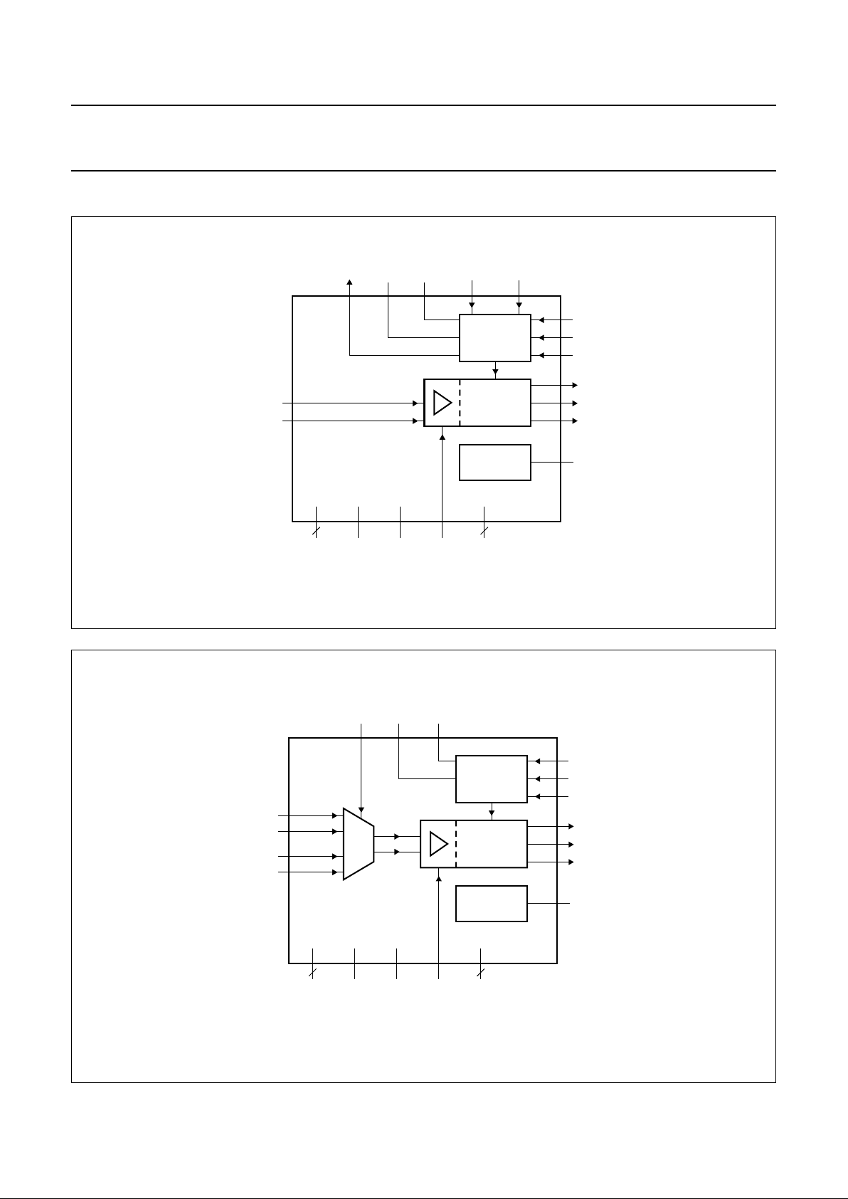
BLOCK DIAGRAM
handbook, full pagewidth
LASER
CONTROL
BLOCK
BAND GAP
REFERENCE
data input
(differential)
TZA3001AHL
CURRENT
SWITCH
ALARMHITZERO
2
DIN
MONIN
28
18
ALARMLO
215
TONE
4
ALARM
26
22
ONE
23
ZERO
13
LA
DINQ
29
12
LAQ
15
BIAS
6
BGAP
MGK271
ALS
31
V
CC(B)
10
GND
1, 3, 8, 9,
11, 14, 16, 17
24, 25, 32
V
CC(G)
7
V
CC(R)
19, 20
27, 30
411
Fig.1 Block diagram of TZA3001AHL.
handbook, full pagewidth
MGK270
LASER
CONTROL
BLOCK
BAND GAP
REFERENCE
TZA3001BHL
CURRENT
SWITCH
MUX
TZERO
ALS
2
DLOOP
MONIN
19
31
V
CC(B)
10
GND
1, 3, 8, 9,
11, 14, 16, 17
24, 25, 32
V
CC(G)
7
ENL
26 5
TONE
4
22
ONE
23
ZERO
13
LA
DLOOPQ
20
DIN
28
DINQ
29
12
LAQ
15
BIAS
6
BGAP
V
CC(R)
18, 21
27, 30
411
Fig.2 Block diagram of TZA3001BHL.
Page 4

2000 Feb 22 4
Philips Semiconductors Product specification
SDH/SONET STM4/OC12 laser drivers
TZA3001AHL; TZA3001BHL;
TZA3001U
PINNING
SYMBOL
PIN PAD
DESCRIPTION
TZA3001AHL TZA3001BHL TZA3001U
GND 1 1 1 ground
MONIN 2 2 2 monitor photodiode current input
GND 3 3 3 ground
IGM −−4 not connected
TONE 4 4 5 connection for external capacitor used for setting
optical 1 control loop time constant (optional)
TZERO 5 5 6 connection for external capacitor used for setting
optical 0 control loop time constant (optional)
BGAP 6 6 7 connection for external band gap decoupling capacitor
V
CC(G)
7 7 8 supply voltage (green domain); note 1
V
CC(G)
−−9 supply voltage (green domain); note 1
GND 8 8 10 ground
GND 9 9 11 ground
V
CC(B)
10 10 12 supply voltage (blue domain); note 2
V
CC(B)
−−13 supply voltage (blue domain); note 2
GND 11 11 14 ground
LAQ 12 12 15 laser modulation output inverted
LA 13 13 16 laser modulation output
GND 14 14 17 ground
BIAS 15 15 18 laser bias current output
GND 16 16 19 ground
GND 17 17 20 ground
GND −−21 ground
ALARMHI 18 − 22 maximum bias current alarm reference level input
V
CC(R)
− 18 23 supply voltage (red domain); note 3
V
CC(R)
19 −−supply voltage (red domain); note 3
DLOOP − 19 24 loop mode data input
V
CC(R)
20 −−supply voltage (red domain); note 3
DLOOPQ − 20 25 loop mode data input inverted
V
CC(R)
−−26 supply voltage (red domain); note 3
ALARMLO 21 − 27 minimum bias current alarm reference level input
V
CC(R)
− 21 − supply voltage (red domain); note 3
ONE 22 22 28 optical 1 reference level input
ZERO 23 23 29 optical 0 reference level input
GND 24 24 30 ground
GND 25 25 31 ground
ALARM 26 − 32 alarm output
ENL − 26 33 loop mode enable input
V
CC(R)
27 27 34 supply voltage (red domain); note 3
Page 5
2000 Feb 22 5
Philips Semiconductors Product specification
SDH/SONET STM4/OC12 laser drivers
TZA3001AHL; TZA3001BHL;
TZA3001U
Notes
1. Supply voltage for the Monitor PhotoDiode (MPD) input current.
2. Supply voltage for the laser modulation outputs (LA, LAQ).
3. Supply voltage for the data inputs (DIN, DINQ), optical 1 and 0 reference level inputs (ONE, ZERO), and the bias
current alarm reference level inputs (ALARMHI, ALARMLO).
DIN 28 28 35 data input
DINQ 29 29 36 data input inverted
V
CC(R)
30 30 37 supply voltage (red domain); note 3
ALS 31 31 38 automatic laser shutdown input
GND 32 32 39 ground
GND −−40 ground
SYMBOL
PIN PAD
DESCRIPTION
TZA3001AHL TZA3001BHL TZA3001U
handbook, full pagewidth
TZA3001AHL
MGK273
1
2
3
4
5
6
7
8
24
23
22
21
20
19
18
17
9
10
11
12
13
14
15
16
32
31
30
29
28
27
26
25
GND
MONIN
GND
TONE
TZERO
BGAP
V
CC(G)
GND
GND
V
CC(B)
GND
LAQ
GND
BIAS
GND
LA
GND
ALARMHI
V
CC(R)
ONE
ALARMLO
ZERO
V
CC(R)
GND
GND
DIN
DINQ
V
CC(R)
ALS
GND
ALARM
V
CC(R)
Fig.3 Pin configuration of TZA3001AHL.
Page 6
2000 Feb 22 6
Philips Semiconductors Product specification
SDH/SONET STM4/OC12 laser drivers
TZA3001AHL; TZA3001BHL;
TZA3001U
handbook, full pagewidth
TZA3001BHL
MGK272
1
2
3
4
5
6
7
8
24
23
22
21
20
19
18
17
9
10
11
12
13
14
15
16
32
31
30
29
28
27
26
25
GND
MONIN
GND
TONE
TZERO
BGAP
V
CC(G)
GND
GND
V
CC(B)
GND
LAQ
GND
BIAS
GND
LA
GND
V
CC(R)
DLOOPQ
ONE
V
CC(R)
ZERO
DLOOP
GND
GND
DIN
DINQ
V
CC(R)
ALS
GND
ENL
V
CC(R)
Fig.4 Pin configuration of TZA3001BHL.
FUNCTIONAL DESCRIPTION
The TZA3001AHL, TZA3001BHL and TZA3001U laser
drivers accept a 622 Mbits/s STM4 Non-Return to Zero
(NRZ) input data stream, and generate an output signal
with sufficient current to drive a solid state Fabry Perot
(FP) or Distributed FeedBack (DFB) laser. They also
contain dual loop control circuitry for stabilizing the true
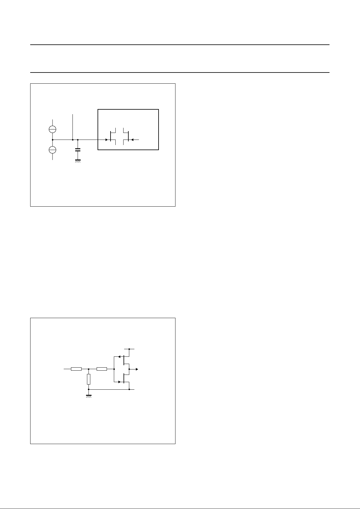
laser optical power levels representing logic 1 and logic 0.
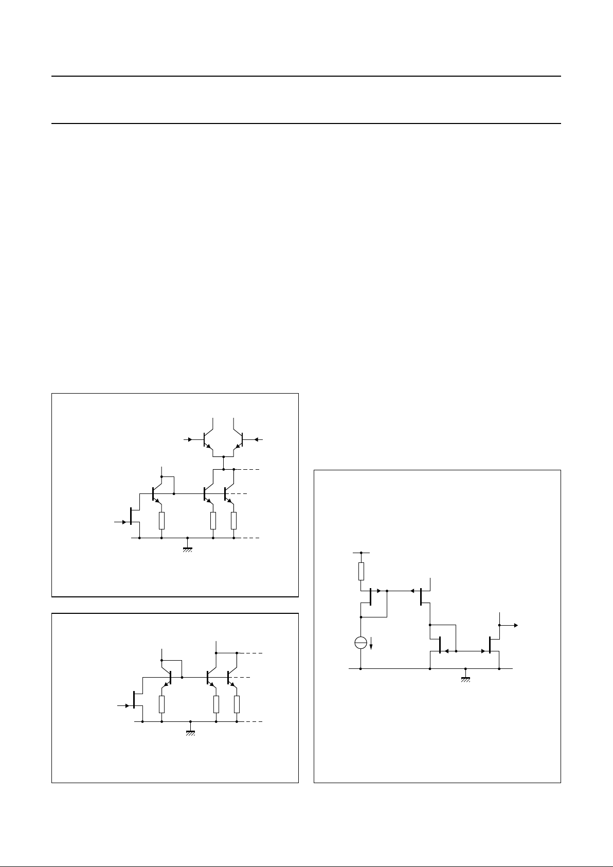
The input buffers present a high impedance to the data
stream on the differential inputs (pins DIN and DINQ);
see Fig.5. The input signal can be at a CML level of
approximately 200 mV (p-p) below the supply voltage, or
at a PECL level up to 800 mV (p-p). The inputs can be
configured to accept CML signals by connecting pins DIN
and DINQ to V
CC(R)
via external 50 Ω pull-up resistors.
If PECL compatibility is required, the usual Thevenin
termination can be applied.
handbook, full pagewidth
MGS910
10 kΩ 10 kΩ
DINQ, DLOOPQDIN, DLOOP
100 Ω
GND
V
CC(R)
100 Ω
Fig.5 DIN/DINQ and DLOOP/DLOOPQ inputs.
Page 7
2000 Feb 22 7
Philips Semiconductors Product specification
SDH/SONET STM4/OC12 laser drivers
TZA3001AHL; TZA3001BHL;
TZA3001U
For ECL signals (negative and referenced to ground), the
inputs should be AC-coupled to the signal source.
If AC-coupling is applied, a constant input signal (either
LOW or HIGH) will cause the device to be in an undefined
state. To avoid this, it is recommended to apply a slight
offset to the input stage. The applied offset must be higher
than the specified value in Chapter “Characteristics”, but
much lower than the applied input voltage swing.
The RF path is fully differential and contains a differential
preamplifier and a main amplifier. The main amplifier is
able to operate at the large peak currents required at the
output laser driver stage and is insensitive to supply
voltage variations. The output signal from the main
amplifier drives a current switch which supplies a
guaranteed maximum modulation current of 60 mA to
pins LA and LAQ (see Fig.6). The BIAS pin outputs a
guaranteed maximum DC bias current of up to 90 mA for
adjusting the optical laser output to a level above its light
emitting threshold (see Fig.7).
Automatic laser control
A laser with a Monitor PhotoDiode (MPD) is required for
the laser control circuit (see application diagrams
Figs 18 and 19).
The MPD current is proportional to the laser emission and
is applied to pin MONIN. The MPD current range is
100 to 1000 µA (p-p).Theinputbufferisoptimizedtocope
with an MPD capacitance of up to 50 pF. To prevent the
input buffer from oscillating if the MPD capacitance is low,
thecapacitanceshouldbeincreasedtotheminimumvalue
specified in Chapter “Characteristics”, by connecting a
capacitor between pin MONIN and V
CC(G)
.
DC reference currents are applied to pins ONE and ZERO
to set the MPD reference levels for laser HIGH and laser
LOW respectively. This is adequately achieved by using
resistors to connect V
CC(R)
to pins ONE and ZERO,
(see Fig.8), however, current DACs can also be used.
The voltages on pins ONE and ZERO are held at a
constantlevelof1.5 VbelowV
CC(R)
.Thereferencecurrent
applied to pin ONE is internally multiplied by 16 and the
reference current flowing into pin ZERO is internally
multipliedby 4. The accuracy of the V
CC(R)
− 1.5 Vvoltage
at pins ONE and ZERO is described in Section “Accuracy
of voltage on inputs: ONE, ZERO, ALARMLO, ALARMHI”.
handbook, halfpage
MGS906
GND
LA LAQ
ALS
TR
TR
n
Fig.6 LA and LAQ outputs.
handbook, halfpage
MGS907
GND
BIAS
ALS
TR
TR
n
Fig.7 Laser driver bias current output circuit.
handbook, halfpage
MGS908
V
CC(R)
GND
ONE, ZERO, ALARMLO, ALARMHI
50 µA
30 kΩ
Fig.8 ONE, ZERO, ALARMLO and ALARMHI
inputs.
Page 8

2000 Feb 22 8
Philips Semiconductors Product specification
SDH/SONET STM4/OC12 laser drivers
TZA3001AHL; TZA3001BHL;
TZA3001U
The reference current and the resistor for the optical 1
modulation current control loop is calculated using the
following formulae:
(1)
(2)
The reference current and resistor for the optical 0 bias
current control loop is calculated using the following
formulae:
(3)
(4)
In these formulae, I
MPD(ONE)
and I
MPD(ZERO)
represent the
MPD current during an optical 1 and an optical 0 period,
respectively.
EXAMPLE
A laser operates at optical output power levels of 0.3 mW
forlaserHIGHand0.03 mW for laser LOW (extinction ratio
of 10 dB). Suppose the corresponding MPD currents for
this particular laser are 260 and 30 µA, respectively.
In this example, the reference current flowing into
pin ONE is:
This current can be set usinga current source or simply by
a resistor of the appropriate value connected between
pin ONE and V
CC(R)
.
In this example, the resistor is:
In this example, the reference current at pin ZERO is:
and can be set using a resistor:
It should be noted that the MPD current is stabilized rather
than the actual laser optical output power. Any deviations
between optical output power and MPD current, known as
‘tracking errors’, cannot be corrected.
Designing the modulation and bias current control
loop
The optical 1 and 0 current control loop time constantsare
determined by on-chip capacitances. If the resulting time
constants are found to be too small in a specific
application, they can be increased by connecting a
capacitor between pins TZERO and TONE.
The optical 1 modulation current control loop time
constant (τ)and bandwidth (B) can be estimatedusing the
following formulae:
(5)
(6)
The optical 0 bias current control loop time constant and
bandwidth can be estimated using the following formulae:
(7)
(8)
The term η
LASER
(dimensionless) in the above formulae is
the product of the following two terms:
•ηEO is the electro-optical efficiency which accounts for
thesteepness of the laser slope characteristic. It defines
the rate at which the optical output powerincreases with
modulation current, and is measured in W/A.
• R is the MPD responsivity. It determines the amount of
MPD current for a given value of optical output power,
and is measured in A/W.
EXAMPLE
A laser with an MPD has the following specifications:
PO= 1 mW, Ith= 25 mA, ηEO= 30 mW/A, R = 500 mA/W.
The term I
th
is the required threshold current to switch on
the laser. If the laser operates just above the threshold
level, it may be assumed that η
EO
near the optical 0 level
is 50% of η
EO
near the optical 1 level, due to the slope
decreasing near the threshold level.
I
ref ONE()
1
16
------
I
MPD(ONE)
×= A[]
R
ONE
1.5
I
ONE
-----------
24
I
MPD(ONE)
------------------------
== Ω[]
I
ref ZERO()
1
4
-- -
I
MPD(ZERO)
×= A[]
R
ZERO
1.5
I
ZERO
--------------
6
I
MPD(ZERO)
---------------------------
== Ω[]
I
ref ONE()
1
16
------
260 10×
6–
× 16.25 µA==
R
ONE
1.5
16.25 106–×
-------------------------------- -
92.3 kΩ==
I
ref ZERO()
1
4
-- -
30 10
6–
×× 7.5 µA==
R
ZERO
1.5
7.5 106–×
--------------------------
200 kΩ==
τ
ONE
40 10
12–
C
TONE
+×()
80 10
3
×
η
LASER
----------------------
×= s[]
B
ONE
1
2πτ
ONE
×
------------------------- -
= Hz[]
B
ONE
η
LASER
2π 40 10
12–
× C
TONE
+()× 80× 103×
-------------------------------------------------------------------------------------------------
Hz[]=
τ
ZERO
40 10
12–
C
TZERO
+×()
50 10
3
×
η
LASER
----------------------
×= s[]
B
ZERO
1
2πτ
ZERO
×
----------------------------
= Hz[]
B
ZERO
η
LASER
2π 40 10
12–
C
TZERO
+×()× 50× 103×
----------------------------------------------------------------------------------------------------
Hz[]=
Page 9
2000 Feb 22 9
Philips Semiconductors Product specification
SDH/SONET STM4/OC12 laser drivers
TZA3001AHL; TZA3001BHL;
TZA3001U
In this example, the resulting bandwidth for the optical 1
modulation current control loop, without an external
capacitor, is:
The resulting bandwidth for the optical 0 bias current
control loop, without an external capacitor, is:
It is not necessary to add additional capacitance with this
type of laser.
Control loop data pattern and bit rate dependency
The constants in equations (1) and (3) are valid when the
data pattern frequently contains a sufficient number of
‘constantzeroes’and‘constantones’.A single control loop
time period (τ
ONE
and τ
ZERO
) must contain ones and zeros
for at least approximately 6 ns (as provided, for example,
by the A1/A2 frame alignment bytes for STM4/OC12).
In practice, the optical extinction ratio increases if the bit
rate increases. Therefore, it is important to use the actual
data patterns and bit rate of the final application circuit for
adjusting the optical levels.
The laser driver peak detectors are able to track MPD
output current overshoot and undershoot conditions.
Unfortunately, these conditions affect the ability of the IC
to correctly interpret the high and low level MPD current.
In particular, the occurrence of undershoot can have a
markedly adverse effect on the interpretation of the low
level MPD current.
Additional bias by modulation ‘off’ current
Although during operation, the full modulation current
switches between outputs LA and LAQ, a small amount of
modulation current continues to flow through the inactive
pin.
For example, when the laser, whose cathode is connected
to LA, is in the ‘dark’ part of its operating cycle (logic 0),
someof the modulation ‘off’ current flows through LA while
most of the current flows through LAQ. This value
I
o(mod)(off)
is effectively added to the bias current and is
subtracted from the modulation current. Fortunately, the
value correlates closely with the magnitude of the
modulation current. Therefore, applications requiring low
bias and low modulation are less affected. Figure 9 shows
the modulation ‘off’ current as a function of the modulation
‘on’ current.
Monitoring the bias and modulation current
Although not recommended, the bias and modulation
currentsgenerated by the laser driver can bemonitored by
measuring the voltages on pins TZERO and TONE,
respectively (see Fig.10). The relationship between these
voltages and the corresponding currents are given as
transconductance values and are specified in
Chapter “Characteristics”. The voltages on pins TZERO
and TONE range from 1.4 to 3.4 V. Any connection to
these pins should have a very high impedance value. It is
mandatory to use a CMOS buffer or an amplifier with an
input impedance higher than 100 GΩ and with an
extremely low input leakage current (pA).
B
ONE
30 103–× 500× 103–×
2π 40× 10
12–
× 80× 103×
---------------------------------------------------------------------
750 Hz≈=
B
ZERO
0.5 30× 103–× 500× 103–×
2π 40× 10
12–
× 50× 103×
-------------------------------------------------------------------------
600 Hz≈=
handbook, halfpage
0 204060
3
1
0
2
MGS902
I
o(mod)(on)
(mA)
(2)
(1)
I
o(mod)(off)
(mA)
Fig.9 I
o(mod)(off)
as a function of I
o(mod)(on)
.
(1) Worst case operation (Tj= 125 °C, VCC= 5.5 V
and worst case parameter processes).
(2) Typical operation.
Page 10
2000 Feb 22 10
Philips Semiconductors Product specification
SDH/SONET STM4/OC12 laser drivers
TZA3001AHL; TZA3001BHL;
TZA3001U
Automatic laser shut-down and laser slow start
The laser modulation and bias currents can be rapidly
switched off when a HIGH level (CMOS) is applied to
pin ALS. This function allows the circuit to be shut-down in
the event of an optical system malfunction. A 25 kΩ
pull-down resistor defaults pin ALS to the non active state
(see Fig.11).
When a LOW level is applied to pin ALS, the modulation
and bias currents slowly increase to the desired values at
the typical time constants of τ
ONE
and τ
ZERO
, respectively.
This can be used to slow-start the laser.
Manual laser override
The automatic laser control function can be overridden by
connecting voltage sources to pins TZERO and TONE to
take direct control of the current sources for bias and
modulation respectively. The control voltages should
range from 1.4 to 3.4 V to swing the modulation current
over the range 1 to 60 mA and the bias current over the
range 1 to 90 mA. These current ranges are guaranteed.
Due to the tolerance range in the manufacturing process,
some devices may have higher current values than those
specified, as shown in Figs 12 and 13. Both figures show
thattemperature changes cause a slight tilting of the linear
characteristic around an input voltage of 2.4 V.
Consequently, the manually controlled current level is
most insensitive to temperature variations at around this
value. Bias and modulation currents in excess of the
specified range are not supported and should be avoided.
Currentsintoor out of pins TZERO and TONE in excess of
10 µA must be avoided to prevent damage to the circuit.
handbook, halfpage
MGS905
GND
40 pF
<
1 nA
LINEAR VOLTAGE TO
CURRENT CONVERTER
TZERO, TONE
2.4 V
<
1 nA
Fig.10 TZERO and TONE internal configuration.
handbook, halfpage
MGS911
25 kΩ
V
CC(R)
100 Ω
GND
ALS
100 Ω
Fig.11 ALS input.
Page 11

2000 Feb 22 11
Philips Semiconductors Product specification
SDH/SONET STM4/OC12 laser drivers
TZA3001AHL; TZA3001BHL;
TZA3001U
handbook, full pagewidth
3.9
160
120
40
0
1.4 1.9 3.4
80
2.9
2.4
MGS904
I
o(mod)
(mA)
V
TONE
(V)
(3)
(4)
(1)
(5)
specified range
(2)
Fig.12 Modulation current with variation in Tj and tolerance range in the manufacturing process.
(1) Tj=25°C (device with characteristics at upper limit of manufacturing tolerance range).
(2) Tj=25°C (typical device).
(3) Tj= −40 °C (typical device).
(4) Tj= 125 °C (typical device).
(5) Tj=25°C (device with characteristics at lower limit of manufacturing tolerance range).
Page 12

2000 Feb 22 12
Philips Semiconductors Product specification
SDH/SONET STM4/OC12 laser drivers
TZA3001AHL; TZA3001BHL;
TZA3001U
handbook, full pagewidth
3.9
160
120
40
0
1.4 1.9 3.4
80
2.9
2.4
MGS903
I
O(BIAS)
(mA)
V
TZERO
(V)
(2)
(3)
(4)
(5)
(1)
specified range
Fig.13 Bias current with variation in Tj and tolerance range in the manufacturing process.
(1) Tj=25°C (device with characteristics at upper limit of manufacturing tolerance range).
(2) Tj=25°C (typical device).
(3) Tj= −40 °C (typical device).
(4) Tj= 125 °C (typical device).
(5) Tj=25°C (device with characteristics at lower limit of manufacturing tolerance range).
Page 13

2000 Feb 22 13
Philips Semiconductors Product specification
SDH/SONET STM4/OC12 laser drivers
TZA3001AHL; TZA3001BHL;
TZA3001U
Bias alarm for TZA3001AHL
The bias current alarm circuit detects whenever the bias
current is outside a predefined range, and generates a
flag. This feature can detect excessive bias current due to
laser ageing or laser malfunctioning. The current applied
to pin ALARMHI should be the maximum permitted bias
current value attenuated by a ratio of 1:1500. The current
applied to pin ALARMLO should be the minimum
permitted bias current value attenuated by a ratio of 1:300.
Like the reference currents for the laser current control
loop, the alarm reference currents can be set by
connecting external resistors between V
CC(R)
and
pins ALARMHI and ALARMLO (see Fig.8). The resistor
values can be calculated using the following formulae:
(9)
(10)
Example: The following reference currents arerequiredto
limit the bias current range from 6 to 90 mA:
and
The corresponding resistor values are:
and
If the alarm condition is true, the voltage on pin ALARM
(see Fig.14) goes to a HIGH level (CMOS). This signal
could be used, for example, to drive pin ALS to disable the
laser driver; the signal to pin ALS has to be latched to
prevent oscillation.
Ahysteresis of approximately 10% is applied toboth alarm
functions. The attenuation ratios of 1:300 and 1:1500 are
valid if the bias current rises above the reference current
levels. If the bias current decreases, the ratios are 10%
lower.
Accuracy of voltage on inputs: ONE, ZERO,
ALARMLO, ALARMHI
It is important to consider the accuracy of the 1.5 V level
with respect to V
CC(R)
on pins ONE and ZERO if resistors
are used to set the reference currents. Although this value
is independent of V
CC(R)
, deviations from 1.5 V can be
caused by:
• Inputcurrent: At Tj=25°C,the voltage between pin and
VCCvaries from 1.58 V atan input current of 6 µA, down
to 1.45 V at 65 µA and 1.41 V at 100 µA. The range
between 65 µA and 100 µA is only specified for
ALARMLO. In the application, the input current is
virtually fixed, so this variation has little effect.
• Variation in batch and individual device characteristics,
not exceeding ±2% from the nominal product: This
variation can be compensated for where devices in the
application are individually trimmed.
• Temperature: The variation in Tj is shown in Fig.15.
At 30 µA (middle of the specified range) the total
variation in Tjis <1%, at 65 µA it is <2% and at 6 µAitis
<3%.
R
ALARMHI
1.5 1500×
I
OBIAS()max()
---------------------------------
= Ω[]
R
ALARMLO
1.5 300×
I
O
BIAS()min()
--------------------------------
= Ω[]
I
ALARMLO
610
3–
×
300
---------------------
20 µA==
I
ALARMHI
90 103–×
1500
------------------------
60 µA==
R
ALARMHI
1.5 1500×
90 103–×
--------------------------- -
25 kΩ==
R
ALARMLO
1.5 300×
610
3–
×
------------------------
75 kΩ==
handbook, halfpage
MGS909
20 Ω
43 Ω
V
CC(R)
GND
ALARM
Fig.14 ALARM output.
Page 14

2000 Feb 22 14
Philips Semiconductors Product specification
SDH/SONET STM4/OC12 laser drivers
TZA3001AHL; TZA3001BHL;
TZA3001U
handbook, full pagewidth
150
−1.65
−1.55
−1.45
−1.60
−1.50
−1.40
−1.35
−50
−40
125
0 10050
MGS901
V
ref
(1)
(V)
Tj (
°C)
(2)
(3)
(4)
(3)
(4)
(2)
(3)
(4)
I
ref =
6 µA
I
ref =
30 µA
I
ref =
65 µA
(2)
Fig.15 V
ref
on pins ONE, ZERO, ALARMLO and ALARMHI with variation in Tj and I
ref
.
(1) Referenced to V
CC(R)
.
(2) Upper limit of manufacturing tolerance range.
(3) Nominal product.
(4) Lower limit of manufacturing tolerance range.
Page 15

2000 Feb 22 15
Philips Semiconductors Product specification
SDH/SONET STM4/OC12 laser drivers
TZA3001AHL; TZA3001BHL;
TZA3001U
Loop mode for TZA3001BHL
The loop mode allows the total system application to be
tested. It allows for uninhibited optical transmission
through the fibre front-end (from the MPD through the
transimpedance stage and the data and clock recovery
unit, to the laser driver and via the laser back to the fibre).
Note that the optical receiver used in conjunction with the
TZA3001BHL must have a loop mode output in order to
complete the test loop.
The loop mode is selected by a HIGH level on pin ENL.
By default, pin ENL is pulled to a LOW level by a 25 kΩ
pull-down resistor (see Fig.16).
Power supply connections
Refer to application diagrams Figs 18 and 19. Three
separate supply domains (labelled V
CC(G)
, V
CC(B)
, and
V
CC(R)
) provide isolation between the MPD current input,
the high-current outputs, and the PECL or CML inputs.
Each supply domain should be connectedto a central V
CC
viaseparatefiltersasshownin Figs 18 and 19.All supply
pins must be connected. The voltage supply levels
should be equal to, and in accordance with, the values
specified in Chapter “Characteristics”.
To maximize power supply isolation, the cathode of the
MPD should be connected to V
CC(G)
and the anode of the
laser diode should be connected to V
CC(B)
. It is
recommended that the laser diode anode is also
connected to a separate decoupling capacitor C9.
Generally, the inverted laser modulation output (pin LAQ)
is not used. To correctly balance the output stage, an
equalization network (Z1) with an impedance comparable
to the laser diode is connected between pin LAQ and
V
CC(B)
.
All external components should be surface mounted
devices, preferably of size 0603 or smaller.
The components must be mounted as close to the IC as
possible.
It is especially recommended to mount the following
components very close to the IC:
• Power supply decoupling capacitors C2, C3 and C4
• Inputmatchingnetworkonpins DIN,DINQ,DLOOPand
DLOOPQ
• Capacitor C5 on pin MONIN
• Output matching network Z1 at the unused output
• The laser.
Bare die ground
In addition to the separate VCC domains, the bare die
contains three corresponding ground (GND) domains.
Isolation between the GND domains is limited due to the
finite substrate conductance.
Mount the die preferably on a large and highly conductive
grounded die pad. All GND pads must be bonded to the
die pad. The external ground is thusideallycombined with
the die ground to avoid ground bounce problems.
Layout recommendations
Layout recommendations for the TZA3001AHL and
TZA3001BHL can be found in application note
“AN98090
Fiber optic transceiverboard STM1/4/8, OC3,12,24,
FC/GE”
.
handbook, halfpage
MGS912
25 kΩ
V
CC(R)
GND
ENL
600 Ω
Fig.16 ENL input.
Page 16

2000 Feb 22 16
Philips Semiconductors Product specification
SDH/SONET STM4/OC12 laser drivers
TZA3001AHL; TZA3001BHL;
TZA3001U
LIMITING VALUES
In accordance with the Absolute Maximum Rating System (IEC 60134).
THERMAL CHARACTERISTICS
SYMBOL PARAMETER MIN. MAX. UNIT
V
CC
supply voltage −0.5 +6 V
V
n
DC voltage on
pin MONIN 1.3 V
CC
+ 0.5 V
pins TONE and TZERO −0.5 V
CC
+ 0.5 V
pin BGAP −0.5 +3.2 V
pin BIAS −0.5 VCC+ 0.5 V
pins LA and LAQ 1.3 V
CC
+ 0.5 V
pin ALS −0.5 V
CC
+ 0.5 V
pins ONE and ZERO −0.5 V
CC
+ 0.5 V
pins DIN and DINQ −0.5 V
CC
+ 0.5 V
pin ALARM (TZA3001AHL) −0.5 V
CC
+ 0.5 V
pins ALARMHI and ALARMLO (TZA3001AHL) −0.5 V
CC
+ 0.5 V
pins DLOOP and DLOOPQ (TZA3001BHL) −0.5 V
CC
+ 0.5 V
pin ENL (TZA3001BHL) −0.5 V
CC
+ 0.5 V
I
n
DC current on
pin MONIN −0.5 +2.5 mA
pins TONE and TZERO −0.5 +0.5 mA
pin BGAP −2.0 +2.5 mA
pin BIAS −0.5 +200 mA
pins LA and LAQ −0.5 +100 mA
pin ALS −0.5 +0.5 mA
pins ONE and ZERO −0.5 +0.5 mA
pins DIN and DINQ −0.5 +0.5 mA
pin ALARM (TZA3001AHL) −0.5 +10 mA
pins ALARMHI and ALARMLO (TZA3001AHL) −0.5 +0.5 mA
pins DLOOP and DLOOPQ (TZA3001BHL) −0.5 +0.5 mA
pin ENL (TZA3001BHL) −0.5 +0.5 mA
T
amb
ambient temperature −40 +85 °C
T
j
junction temperature −40 +125 °C
T
stg
storage temperature −65 +150 °C
SYMBOL PARAMETER VALUE UNIT
R
th(j-s)
thermal resistance from junction to solder point 15 K/W
R
th(j-c)
thermal resistance from junction to case 23 K/W
Page 17

2000 Feb 22 17
Philips Semiconductors Product specification
SDH/SONET STM4/OC12 laser drivers
TZA3001AHL; TZA3001BHL;
TZA3001U
CHARACTERISTICS
VCC= 4.5 to 5.5 V; T
amb
= −40 to +85 °C; all voltages measured with respect to GND.
SYMBOL PARAMETER CONDITIONS MIN. TYP. MAX. UNIT
Supply
V
CC
supply voltage 4.5 5.0 5.5 V
I
CC(R)
supply current (R) − 410 mA
I
CC(G)
supply current (G) 12 18 26 mA
I
CC(B)
supply current (B) ALS LOW; note 1 20 41 65 mA
ALS HIGH − 35 mA
I
CC(tot)
total supply current ALS LOW; note 1 32 63 101 mA
ALS HIGH 12 25 41 mA
P
tot
total power dissipation ALS LOW; note 2 145 430 925 mW
ALS HIGH; note 2 50 125 225 mW
Data inputs: pins DIN and DINQ (and pins DLOOP and DLOOPQ on TZA3001BHL); (see Fig.17)
V
i(p-p)
input voltage
(peak-to-peak value)
single-ended 100 250 800 mV
V
IO
input offset voltage −25 − +25 mV
V
I(min)
minimum input voltage V
CC(R)
− 2 −− V
V
I(max)
maximum input voltage −−V
CC(R)
+ 0.25 V
Z
i
input impedance for low frequencies;
single-ended
71013kΩ
CMOS inputs: pin ALS (and pin ENL on TZA3001BHL)
V
IL
LOW-level input voltage −−2V
V
IH
HIGH-level input voltage 3 −− V
R
pd(ALS)
internal pull-down
resistance on pin ALS
21 25.5 30 kΩ
R
pd(ENL)
internal pull-down
resistance on pin ENL
15 25 35 kΩ
CMOS output: pin ALARM (on TZA3001AHL)
V
OL
LOW-level output voltage IOH= −200 µA0−0.2 V
V
OH
HIGH-level output voltage IOH= 200 µAV
CC
− 0.2 − V
CC
V
Monitor photodiode input: pin MONIN
V
I
DC input voltage 1.2 1.8 2.4 V
I
MPD
monitor photodiode
current
laser optical 0 24 − 260 µA
laser optical 1 96 − 1040 µA
C
MPD
monitor photodiode
capacitance
note 3 30 − 50 pF
Page 18

2000 Feb 22 18
Philips Semiconductors Product specification
SDH/SONET STM4/OC12 laser drivers
TZA3001AHL; TZA3001BHL;
TZA3001U
Control loop reference current inputs: pins ONE and ZERO
I
ref(ONE)
reference current on
pin ONE
note 4 6 − 65 µA
V
ref(ONE)
reference voltage on
pin ONE
referenced to V
CC(R)
;
note 5
−−1.5 − V
α
(ONE)
attenuationratioofI
ref(ONE)
to I
MPD(ONE)
note 6 − 16 −−
I
ref(ZERO)
reference current on
pin ZERO
note 4 6 − 65 µA
V
ref(ZERO)
reference voltage on
pin ZERO
referenced to V
CC(R)
;
note 5
−−1.5 − V
α
(ZERO)
attenuation ratio of
I
ref(ZERO)
to I
MPD(ZERO)
note 6 − 4 −−
Control loop time constants: pins TONE and TZERO
V
TONE
voltage on pin TONE floating output 1.4 − 3.4 V
g
m(TONE)
transconductance of
pin TONE
note 7 60 95 130 mA/V
V
TZERO
voltage on pin TZERO floating output 1.4 − 3.4 V
g
m(TZERO)
transconductance of
pin TZERO
note 8 100 145 190 mA/V
Laser modulation current outputs: pins LA and LAQ
I
o(mod)(on)
modulation output current
(active pin)
note 9 2.5 − 60 mA
I
o(mod)(off)
modulation output current
(inactive pin)
I
o(mod)(on)
= 30mA −−0.5 mA
I
o(mod)(on)
= 60mA −−2.8 mA
I
o(mod)(ALS)
output current during laser
shutdown
−−10 µA
V
O
output voltage 2 − 5V
t
r
current rise time note 10 − 120 300 ps
t
f
current fall time note 10 − 120 300 ps
J
o(p-p)
intrinsic electrical output
jitter (peak-to-peak value)
note 11 −−50 mUI
Laser bias current output: pin BIAS
I
O(BIAS)
bias output current note 12 2.8 − 90 mA
I
O(BIAS)(ALS)
output current during laser
shutdown
−−10 µA
t
res(off)
response time after laser
shutdown
I
O(BIAS)
= 90 mA; note 13 −−1µs
V
O(BIAS)
bias output voltage 1 − 5V
SYMBOL PARAMETER CONDITIONS MIN. TYP. MAX. UNIT
Page 19

2000 Feb 22 19
Philips Semiconductors Product specification
SDH/SONET STM4/OC12 laser drivers
TZA3001AHL; TZA3001BHL;
TZA3001U
Notes
1. Supply current:
a) The values do not include the modulation and bias currents through pins LA, LAQ and BIAS.
b) Minimum value refers to V
TONE
= 1.4 V at I
o(mod)(min)
and V
TZERO
= 1.4 V at I
O(BIAS)(min)
.
c) Maximum value refers to V
TONE
= 3.4 V at I
o(mod)(max)
and V
TZERO
= 3.4 V at I
O(BIAS)(max)
.
d) A first order estimate of the typical value of I
CC(tot)
as a function of Tj, I
o(mod)
, and I
O(BIAS)
is:
I
CC(tot)
= .
2. Power dissipation:
a) The value for P
tot
includes the modulation and bias currents through pins LA, LAQ and BIAS.
b) The minimum value for P
tot
is the on-chip dissipation when V
TONE
= 1.4 V at I
o(mod)(min)
, VLA=V
LAQ
=2V,
V
TZERO
= 1.4 V at I
O(BIAS)(min)
, V
O(BIAS)
= 1 V, and parameter processes are at a minimum.
c) The maximum value for P
tot
is the on-chip dissipation when V
TONE
= 3.4 V at I
o(mod)(max)
, VLA=V
LAQ
=2V,
V
TZERO
= 3.4 V at I
O(BIAS)(max)
, V
O(BIAS)
= 1 V, and parameter processes are at a maximum.
d) P
tot=ICC(tot)
× VCC+I
O(BIAS)
× V
O(BIAS)+ILA
× VLA with I
o(mod)(on)
flowing through pin LA.
3. The minimum value of the capacitance on pin MONIN is required to prevent instability.
4. The reference currents can be set by connecting external resistors between VCC and pins ONE and ZERO
(see Section “Automatic laser control”). The corresponding MPD current range for optical 1 is from 96 to 1040 µA.
The MPD current range for optical 0 is from 24 to 260 µA.
5. See Section “Accuracy of voltage on inputs: ONE, ZERO, ALARMLO, ALARMHI”.
6. See Section “Automatic laser control”.
7. The specified transconductance is the ratio between the modulation current on pins LA or LAQ and the voltage on
pin TONE, under small signal conditions.
Alarm reference current inputs: pins ALARMHI and ALARMLO (TZA3001AHL)
I
ref(ALARMLO)
reference current on
pin ALARMLO
note 14 6 − 100 µA
V
ref(ALARMLO)
reference voltage on
pin ALARMLO
referenced to V
CC(R)
−−1.5 − V
α
(ALARMLO)
attenuation ratio of
I
ref(ALARMLO)
to I
O(BIAS)(min)
note 15 200 315 400
I
O(BIAS)(min)(hys)
minimum bias current
detection hysteresis
7.5 10 15 %
I
ref(ALARMHI)
reference current on
pin ALARMHI
note 14 6 − 65 µA
V
ref(ALARMHI)
reference voltage on
pin ALARMHI
referenced to V
CC(R)
−−1.5 − V
α
(ALARMHI)
attenuation ratio of
I
ref(ALARMHI)
to I
O(BIAS)(max)
note 15 1300 1500 1700
I
O(BIAS)(max)(hys)
maximum bias current
detection hysteresis
7.5 10 15 %
Reference voltage output: pin BGAP
V
O
output voltage 1.165 1.20 1.235 µA
SYMBOL PARAMETER CONDITIONS MIN. TYP. MAX. UNIT
55.6 mA 0.0015+ I
OBIAS()
mA[]I
o mod()on()
mA[]×× 1 0.026
T
j
°C[]
25
-----------------
×–
×
Page 20

2000 Feb 22 20
Philips Semiconductors Product specification
SDH/SONET STM4/OC12 laser drivers
TZA3001AHL; TZA3001BHL;
TZA3001U
8. The specified transconductance is the ratio between the bias current on pin BIAS and the voltage on pin TZERO,
under small signal conditions.
9. These are the guaranteed values; the lowest attainable output current will always be lower than 2.5 mA, and the
highest output current will always be higher than 60 mA.
10. The voltage rise and fall times (20% to 80%) can have larger values due to capacitive effects. Specifications are
guaranteed by design and characterization. Each device is tested at full operating speed to guarantee RF
functionality.
11. Measured in a frequency band from 250 kHz to 5 MHz, according to
“ITU-T Recommendation G.813”
.
The electrically generated (current) jitter is assumed to be less than 50% of the optical output jitter. The specification
is guaranteed by design.
12. These are the guaranteed values; the lowest output current will always be less than 2.8 mA and the highest output
current will always be more than 90 mA.
13. The response time is defined as the delay between the onset of the ramp on pin ALS (at 10% of the HIGH-level) and
the extinction of the bias current (at 10% of the original value).
14. The reference currents can be set by connecting a resistor between pin ALARMLO and V
CC(R)
and between
pin ALARMHI and V
CC(R)
; for detailed information, see Section “Bias alarm for TZA3001AHL”. The corresponding
low-bias threshold range is 1.8 to 19.5 mA. The high-bias threshold range is 9 to 97.5 mA.
15. See Section “Bias alarm for TZA3001AHL”.
handbook, full pagewidth
MGK274
V
IO
V
I(max)
V
I(min)
V
i(p-p)
V
CC(R)
Fig.17 Logic level symbol definitions for data inputs.
Page 21

2000 Feb 22 21
Philips Semiconductors Product specification
SDH/SONET STM4/OC12 laser drivers
TZA3001AHL; TZA3001BHL;
TZA3001U
APPLICATION INFORMATION
handbook, full pagewidth
MGK276
R5
18 Ω
TZA3001AHL
V
CC(R)
TONE
MONIN
11
C6
(3)
TZERO
C7
(4)
BGAP
22 nF
C8
2
4
5
6
1, 3, 8, 9, 11,
14, 16, 17,
24, 25, 32
15 13 12
GND BIAS LA LAQ
19, 20,
27, 30
V
CC(B)
V
CC(G)
ALS
31710
DINQ29DIN28ALARM
R1
(5)R2(5)R3(6)R4(6)
26
23
22
data inputs
normal mode
(CML/PECL compatible)
21
18
ALARMHI
laser
C9
MPD
ALARMLO
Z1
(7)
C5
(2)
L1
4
ONE
ZERO
C2
22 nF
V
CC
C1
1 µF
C3
22 nF
C4
22 nF
(1)
(1)
(1)
Fig.18 Application diagram showing the TZA3001AHL configured for 622 Mbits/s (STM4/OC12).
(1) Ferrite bead e.g. Murata BLM31A601S.
(2) C5 is required to meet the minimum capacitance value on pin MONIN (optional, see Section “Automatic laser control”).
(3) C6 enhances modulation control loop time constant (optional).
(4) C7 enhances bias control loop time constant (optional).
(5) R1 and R2 are used for setting optical 0 and optical 1 reference currents (see Section “Automatic laser control”).
(6) R3 and R4 are used for setting minimum and maximum bias currents (see Section “Bias alarm for TZA3001AHL”).
(7) Z1 is required for balancing the output stage (see Section “Power supply connections”).
Page 22

2000 Feb 22 22
Philips Semiconductors Product specification
SDH/SONET STM4/OC12 laser drivers
TZA3001AHL; TZA3001BHL;
TZA3001U
handbook, full pagewidth
MGK275
R3
18 Ω
TZA3001BHL
V
CC(R)
TONE
MONIN
11
C6
(3)
TZERO
C7
(4)
BGAP
22 nF
C8
2
4
5
6
1, 3, 8, 9, 11,
14, 16, 17,
24, 25, 32
15 13 12
GND BIAS LA LAQ
18, 21,
27, 30
V
CC(B)
V
CC(G)
ALS
31710
DINQ29DIN28ENL
R1
(5)R2(5)
26
23
22
data inputs
normal mode
(CML/PECL compatible)
20
19
laser
C9
MPD
Z1
(6)
C5
(2)
L1
4
ONE
ZERO
C2
22 nF
(1)
V
CC
C1
1 µF
C3
22 nF
C4
22 nF
loop mode inputs
(CML/PECL
compatible)
DLOOP
DLOOPQ
(1)
(1)
Fig.19 Application diagram showing the TZA3001BHL configured for 622 Mbits/s (STM4/OC12).
(1) Ferrite bead e.g. Murata BLM31A601S.
(2) C5 is required to meet the minimum capacitance value on pin MONIN (optional, see Section “Automatic laser control”).
(3) C6 enhances modulation control loop time constant (optional).
(4) C7 enhances bias control loop time constant (optional).
(5) R1 and R2 are used for setting optical 0 and optical 1 reference currents (see Section “Automatic laser control”).
(6) Z1 is required for balancing the output stage (see Section “Power supply connections”).
Page 23

2000 Feb 22 23
Philips Semiconductors Product specification
SDH/SONET STM4/OC12 laser drivers
TZA3001AHL; TZA3001BHL;
TZA3001U
BONDING PAD LOCATIONS
Note
1. All x and y coordinates represent the position of the
centreofthe pad in µm with respect to the centreofthe
die (see Fig.20).
SYMBOL PAD
COORDINATES
(1)
xy
GND 1 −664 −910
MONIN 2 −524 −910
GND 3 −367 −910
IGM 4 −227 −910
TONE 5 −70 −910
TZERO 6 +87 −910
BGAP 7 +244 −910
V
CC(G)
8 +384 −910
V
CC(G)
9 +524 −910
GND 10 +664 −910
GND 11 +910 −630
V
CC(B)
12 +910 −490
V
CC(B)
13 +910 −350
GND 14 +910 −210
LAQ 15 +910 −70
LA 16 +910 +70
GND 17 +910 +210
BIAS 18 +910 +350
GND 19 +910 +490
GND 20 +910 +630
GND 21 +681 +910
ALARMHI 22 +541 +910
V
CC(R)
23 +384 +910
DLOOP 24 +227 +910
DLOOPQ 25 +87 +910
V
CC(R)
26 −70 +910
ALARMLO 27 −210 +910
ONE 28 −367 +910
ZERO 29 −524 +910
GND 30 −681 +910
GND 31 −910 +681
ALARM 32 −910 +541
ENL 33 −910 +384
V
CC(R)
34 −910 +227
DIN 35 −910 +70
DINQ 36 −910 −70
V
CC(R)
37 −910 −227
ALS 38 −910 −367
GND 39 −910 −551
GND 40 −910 −664
SYMBOL PAD
COORDINATES
(1)
xy
Page 24

2000 Feb 22 24
Philips Semiconductors Product specification
SDH/SONET STM4/OC12 laser drivers
TZA3001AHL; TZA3001BHL;
TZA3001U
handbook, full pagewidth
MGL192
y
2 mm
(1)
x
0
0
TZA3001U
1 2 3 4 5 109876
30 29 28 27 26 21
2 mm
(1)
22232425
35
36
37
38
40
39
31
32
33
34
16
15
14
13
11
12
20
19
18
17
TONE
IGM
GND
MONIN
GND
GND
V
CC(G)
V
CC(G)
BGAP
TZERO
ALARMLO
ZERO
GND
ONE
LAQ
V
CC(B)
V
CC(B)
GND
ALS
GND
GND
LA
GND
BIAS
GND
GND
GND
ENL
ALARM
GND
V
CC(R)
DINQ
DIN
V
CC(R)
GND
ALARMHI
V
CC(R)
DLOOP
DLOOPQ
V
CC(R)
Fig.20 Bonding pad locations of TZA3001U.
(1) Typical value.
Table 1 Physical characteristics of bare die
PARAMETER VALUE
Glass passivation 2.1 µm PSG (PhosphoSilicate Glass) on top of 0.7 µm silicon nitride
Bonding pad dimension minimum dimension of exposed metallization is 90 × 90 µm (pad size = 100 × 100 µm)
Metallization 1.2 µm AlCu (1% Cu)
Thickness 380 µm nominal
Size 2.000 × 2.000 mm (4.000 mm
2
)
Backing silicon; electrically connected to GND potential through substrate contacts
Attach temperature <430 °C; glue is recommended for attaching die
Attach time <15 s
Page 25

2000 Feb 22 25
Philips Semiconductors Product specification
SDH/SONET STM4/OC12 laser drivers
TZA3001AHL; TZA3001BHL;
TZA3001U
PACKAGE OUTLINE
0.2
UNIT
A
max.
A
1A2A3bp
cE
(1)
eH
E
LL
p
Zywv θ
REFERENCES
OUTLINE
VERSION
EUROPEAN
PROJECTION
ISSUE DATE
IEC JEDEC EIAJ
mm
1.60
0.15
0.05
1.5
1.3
0.25
0.27
0.17
0.18
0.12
5.1
4.9
0.5
7.15
6.85
1.0
0.95
0.55
7
0
o
o
0.12 0.1
DIMENSIONS (mm are the original dimensions)
Note
1. Plastic or metal protrusions of 0.25 mm maximum per side are not included.
0.75
0.45
SOT401-1 136E01 MS-026
99-12-27
00-01-19
D
(1) (1)(1)
5.1
4.9
H
D
7.15
6.85
E
Z
0.95
0.55
D
b
p
e
E
B
8
D
H
b
p
E
H
v M
B
D
Z
D
A
Z
E
e
v M
A
X
1
32
25
24
17
16
9
θ
A
1
A
L
p
detail X
L
(A )
3
A
2
y
w M
w M
0 2.5 5 mm
scale
LQFP32: plastic low profile quad flat package; 32 leads; body 5 x 5 x 1.4 mm
SOT401-1
c
pin 1 index
Page 26

2000 Feb 22 26
Philips Semiconductors Product specification
SDH/SONET STM4/OC12 laser drivers
TZA3001AHL; TZA3001BHL;
TZA3001U
SOLDERING
Introduction to soldering surface mount packages
Thistextgivesaverybriefinsight to a complex technology.
A more in-depth account of soldering ICs can be found in
our
“Data Handbook IC26; Integrated Circuit Packages”
(document order number 9398 652 90011).
There is no soldering method that is ideal for all surface
mount IC packages. Wave soldering is not alwayssuitable
for surface mount ICs, or for printed-circuit boards with
high population densities. In these situations reflow
soldering is often used.
Reflow soldering
Reflow soldering requires solder paste (a suspension of
fine solder particles, flux and binding agent) to be applied
tothe printed-circuit board by screen printing, stencilling or
pressure-syringe dispensing before package placement.
Several methods exist for reflowing; for example,
infrared/convection heating in a conveyor type oven.
Throughput times (preheating, soldering and cooling) vary
between 100 and 200 seconds depending on heating
method.
Typical reflow peak temperatures range from
215 to 250 °C. The top-surface temperature of the
packages should preferable be kept below 230 °C.
Wave soldering
Conventional single wave soldering is not recommended
forsurfacemountdevices(SMDs)orprinted-circuitboards
with a high component density, as solder bridging and
non-wetting can present major problems.
To overcome these problems the double-wave soldering
method was specifically developed.
If wave soldering is used the following conditions must be
observed for optimal results:
• Use a double-wave soldering method comprising a
turbulent wave with high upward pressure followed by a
smooth laminar wave.
• For packages with leads on two sides and a pitch (e):
– larger than or equal to 1.27 mm, the footprint
longitudinal axis is preferred to be parallel to the
transport direction of the printed-circuit board;
– smaller than 1.27 mm, the footprint longitudinal axis
must be parallel to the transport direction of the
printed-circuit board.
The footprint must incorporate solder thieves at the
downstream end.
• Forpackageswithleadsonfoursides,thefootprintmust
be placed at a 45° angle to the transport direction of the
printed-circuit board. The footprint must incorporate
solder thieves downstream and at the side corners.
During placement and before soldering, the package must
be fixed with a droplet of adhesive. The adhesive can be
applied by screen printing, pin transfer or syringe
dispensing. The package can be soldered after the
adhesive is cured.
Typical dwell time is 4 seconds at 250 °C.
A mildly-activated flux will eliminate the need for removal
of corrosive residues in most applications.
Manual soldering
Fix the component by first soldering two
diagonally-opposite end leads. Use a low voltage (24 V or
less) soldering iron applied to the flat part of the lead.
Contact time must be limited to 10 seconds at up to
300 °C.
When using a dedicated tool, all other leads can be
soldered in one operation within 2 to 5 seconds between
270 and 320 °C.
Page 27

2000 Feb 22 27
Philips Semiconductors Product specification
SDH/SONET STM4/OC12 laser drivers
TZA3001AHL; TZA3001BHL;
TZA3001U
Suitability of surface mount IC packages for wave and reflow soldering methods
Notes
1. All surface mount (SMD) packages are moisture sensitive. Depending upon the moisture content, the maximum
temperature (with respect to time) and body size of the package, there is a risk that internal or external package
cracks may occur due to vaporization of the moisture in them (the so called popcorn effect). For details, refer to the
Drypack information in the
“Data Handbook IC26; Integrated Circuit Packages; Section: Packing Methods”
.
2. These packages are not suitable for wave soldering as a solder joint between the printed-circuit board and heatsink
(at bottom version) can not be achieved, and as solder may stick to the heatsink (on top version).
3. If wave soldering is considered, then the package must be placed at a 45° angle to the solder wave direction.
The package footprint must incorporate solder thieves downstream and at the side corners.
4. Wave soldering is only suitable for LQFP, TQFP and QFP packages with a pitch (e) equal to or larger than 0.8 mm;
it is definitely not suitable for packages with a pitch (e) equal to or smaller than 0.65 mm.
5. Wave soldering is only suitable for SSOP and TSSOP packages with a pitch (e) equal to or larger than 0.65 mm; it is
definitely not suitable for packages with a pitch (e) equal to or smaller than 0.5 mm.
PACKAGE
SOLDERING METHOD
WAVE REFLOW
(1)
BGA, LFBGA, SQFP, TFBGA not suitable suitable
HLQFP, HSQFP, HSOP, HTQFP, HTSSOP, SMS not suitable
(2)
suitable
PLCC
(3)
, SO, SOJ suitable suitable
LQFP, QFP, TQFP not recommended
(3)(4)
suitable
SSOP, TSSOP, VSO not recommended
(5)
suitable
Page 28

2000 Feb 22 28
Philips Semiconductors Product specification
SDH/SONET STM4/OC12 laser drivers
TZA3001AHL; TZA3001BHL;
TZA3001U
DEFINITIONS
LIFE SUPPORT APPLICATIONS
These products are not designed for use in life support appliances, devices, or systems where malfunction of these
products can reasonably be expected to result in personal injury. Philips customers using or selling these products for
use in such applications do so at their own risk and agree to fully indemnify Philips for any damages resulting from such
improper use or sale.
BARE DIE DISCLAIMER
All die are tested and are guaranteed to comply with all data sheet limits up to the point of wafer sawing for a period of
ninety (90) days from the date of Philips' delivery. If there are data sheet limits not guaranteed, these will be separately
indicated in the datasheet. There are no post packing tests performed on individualdie or wafer. Philips Semiconductors
has no control of third party procedures in the sawing, handling, packing or assembly of the die. Accordingly, Philips
Semiconductorsassumes no liability for device functionalityor performance of the die orsystemsafter third party sawing,
handling, packing or assembly of the die. It is the responsibility of the customer to test and qualify their application in
which the die is used.
Data sheet status
Objective specification This data sheet contains target or goal specifications for product development.
Preliminary specification This data sheet contains preliminary data; supplementary data may be published later.
Product specification This data sheet contains final product specifications.
Limiting values
Limiting values given are in accordance with the Absolute Maximum Rating System (IEC 60134). Stress above one or
more of the limiting values may cause permanent damage to the device. These are stress ratings only and operation
of the device at these or at any other conditions above those given in the Characteristics sections of the specification
is not implied. Exposure to limiting values for extended periods may affect device reliability.
Application information
Where application information is given, it is advisory and does not form part of the specification.
Page 29

2000 Feb 22 29
Philips Semiconductors Product specification
SDH/SONET STM4/OC12 laser drivers
TZA3001AHL; TZA3001BHL;
TZA3001U
NOTES
Page 30

2000 Feb 22 30
Philips Semiconductors Product specification
SDH/SONET STM4/OC12 laser drivers
TZA3001AHL; TZA3001BHL;
TZA3001U
NOTES
Page 31

2000 Feb 22 31
Philips Semiconductors Product specification
SDH/SONET STM4/OC12 laser drivers
TZA3001AHL; TZA3001BHL;
TZA3001U
NOTES
Page 32

© Philips Electronics N.V. SCA
All rights are reserved. Reproduction in whole or in part is prohibited without the prior written consent of the copyright owner.
The information presented in this document does not form part of any quotation or contract, is believed to be accurate and reliable and may be changed
without notice. No liability will be accepted by the publisher for any consequence of its use. Publication thereof does not convey nor imply any license
under patent- or other industrial or intellectual property rights.
Internet: http://www.semiconductors.philips.com
2000
69
Philips Semiconductors – a w orldwide compan y
For all other countries apply to: Philips Semiconductors,
International Marketing & Sales Communications, Building BE-p, P.O. Box 218,
5600 MD EINDHOVEN, The Netherlands, Fax. +31 40 27 24825
Argentina: see South America
Australia: 3 Figtree Drive, HOMEBUSH, NSW 2140,
Tel. +61 2 9704 8141, Fax. +61 2 9704 8139
Austria: Computerstr. 6, A-1101 WIEN, P.O. Box 213,
Tel. +43 1 60 101 1248, Fax. +43 1 60 101 1210
Belarus: Hotel Minsk Business Center, Bld. 3, r. 1211, Volodarski Str. 6,
220050 MINSK, Tel. +375 172 20 0733, Fax. +375 172 20 0773
Belgium: see The Netherlands
Brazil: see South America
Bulgaria: Philips Bulgaria Ltd., Energoproject, 15th floor,
51 James Bourchier Blvd., 1407 SOFIA,
Tel. +359 2 68 9211, Fax. +359 2 68 9102
Canada: PHILIPS SEMICONDUCTORS/COMPONENTS,
Tel. +1 800 234 7381, Fax. +1 800 943 0087
China/Hong Kong: 501 Hong Kong Industrial Technology Centre,
72 Tat Chee Avenue, Kowloon Tong, HONG KONG,
Tel. +852 2319 7888, Fax. +852 2319 7700
Colombia: see South America
Czech Republic: see Austria
Denmark: Sydhavnsgade 23, 1780 COPENHAGEN V,
Tel. +45 33 29 3333, Fax. +45 33 29 3905
Finland: Sinikalliontie 3, FIN-02630 ESPOO,
Tel. +358 9 615 800, Fax. +358 9 6158 0920
France: 51 Rue Carnot, BP317, 92156 SURESNES Cedex,
Tel. +33 1 4099 6161, Fax. +33 1 4099 6427
Germany: Hammerbrookstraße 69, D-20097 HAMBURG,
Tel. +49 40 2353 60, Fax. +49 40 2353 6300
Hungary: see Austria
India: Philips INDIA Ltd, Band Box Building, 2nd floor,
254-D, Dr. Annie Besant Road, Worli, MUMBAI 400 025,
Tel. +91 22 493 8541, Fax. +91 22 493 0966
Indonesia: PT Philips DevelopmentCorporation, Semiconductors Division,
Gedung Philips, Jl. Buncit Raya Kav.99-100, JAKARTA 12510,
Tel. +62 21 794 0040 ext. 2501, Fax. +62 21 794 0080
Ireland: Newstead, Clonskeagh, DUBLIN 14,
Tel. +353 1 7640 000, Fax. +353 1 7640 200
Israel: RAPAC Electronics, 7 Kehilat Saloniki St, PO Box 18053,
TEL AVIV 61180, Tel. +972 3 645 0444, Fax. +972 3 649 1007
Italy: PHILIPS SEMICONDUCTORS,ViaCasati, 23 - 20052 MONZA (MI),
Tel. +39 039 203 6838, Fax +39 039 203 6800
Japan: Philips Bldg 13-37, Kohnan 2-chome, Minato-ku,
TOKYO 108-8507, Tel. +81 3 3740 5130, Fax. +81 3 3740 5057
Korea: Philips House, 260-199 Itaewon-dong, Yongsan-ku, SEOUL,
Tel. +82 2 709 1412, Fax. +82 2 709 1415
Malaysia: No. 76 Jalan Universiti, 46200 PETALING JAYA, SELANGOR,
Tel. +60 3 750 5214, Fax. +60 3 757 4880
Mexico: 5900 Gateway East, Suite 200, EL PASO, TEXAS 79905,
Tel. +9-5 800 234 7381, Fax +9-5 800 943 0087
Middle East: see Italy
Netherlands: Postbus 90050, 5600 PB EINDHOVEN, Bldg. VB,
Tel. +31 40 27 82785, Fax. +31 40 27 88399
New Zealand: 2 Wagener Place, C.P.O. Box 1041, AUCKLAND,
Tel. +64 9 849 4160, Fax. +64 9 849 7811
Norway: Box 1, Manglerud 0612, OSLO,
Tel. +47 22 74 8000, Fax. +47 22 74 8341
Pakistan: see Singapore
Philippines: Philips Semiconductors Philippines Inc.,
106 Valero St. Salcedo Village, P.O. Box 2108 MCC, MAKATI,
Metro MANILA, Tel. +63 2 816 6380, Fax. +63 2 817 3474
Poland: Al.Jerozolimskie 195 B, 02-222 WARSAW,
Tel. +48 22 5710 000, Fax. +48 22 5710 001
Portugal: see Spain
Romania: see Italy
Russia: Philips Russia, Ul. Usatcheva 35A, 119048 MOSCOW,
Tel. +7 095 755 6918, Fax. +7 095 755 6919
Singapore: Lorong 1, Toa Payoh, SINGAPORE 319762,
Tel. +65 350 2538, Fax. +65 251 6500
Slovakia: see Austria
Slovenia: see Italy
South Africa: S.A. PHILIPS Pty Ltd., 195-215 Main Road Martindale,
2092 JOHANNESBURG, P.O. Box 58088 Newville 2114,
Tel. +27 11 471 5401, Fax. +27 11 471 5398
South America: Al. Vicente Pinzon, 173, 6th floor,
04547-130 SÃO PAULO, SP, Brazil,
Tel. +55 11 821 2333, Fax. +55 11 821 2382
Spain: Balmes 22, 08007 BARCELONA,
Tel. +34 93 301 6312, Fax. +34 93 301 4107
Sweden: Kottbygatan 7, Akalla, S-16485 STOCKHOLM,
Tel. +46 8 5985 2000, Fax. +46 8 5985 2745
Switzerland: Allmendstrasse 140, CH-8027 ZÜRICH,
Tel. +41 1 488 2741 Fax. +41 1 488 3263
Taiwan: Philips Semiconductors, 6F, No. 96, Chien Kuo N. Rd., Sec. 1,
TAIPEI, Taiwan Tel. +886 2 2134 2886, Fax. +886 2 2134 2874
Thailand: PHILIPS ELECTRONICS (THAILAND) Ltd.,
209/2 Sanpavuth-Bangna Road Prakanong, BANGKOK 10260,
Tel. +66 2 745 4090, Fax. +66 2 398 0793
Turkey: Yukari Dudullu, Org. San. Blg., 2.Cad. Nr. 28 81260 Umraniye,
ISTANBUL, Tel. +90 216 522 1500, Fax. +90 216 522 1813
Ukraine: PHILIPS UKRAINE, 4 Patrice Lumumba str., Building B, Floor 7,
252042 KIEV, Tel. +380 44 264 2776, Fax. +380 44 268 0461
United Kingdom: Philips Semiconductors Ltd., 276 Bath Road, Hayes,
MIDDLESEX UB3 5BX, Tel. +44 208 730 5000, Fax. +44 208 754 8421
United States: 811 East Arques Avenue, SUNNYVALE, CA 94088-3409,
Tel. +1 800 234 7381, Fax. +1 800 943 0087
Uruguay: see South America
Vietnam: see Singapore
Yugoslavia: PHILIPS, Trg N. Pasica 5/v, 11000 BEOGRAD,
Tel. +381 11 3341 299, Fax.+381 11 3342 553
Printed in The Netherlands 403510/150/05/pp32 Date of release: 2000 Feb 22 Document order number: 9397 750 06893
 Loading...