

Page 1

查询TZA3000供应商
INTEGRATED CIRCUITS
DATA SH EET
TZA3000
SDH/SONET STM4/OC12 optical
receiver
Objective specification
File under Integrated Circuits, IC19
1997 Oct 17
Page 2

Philips Semiconductors Objective specification
SDH/SONET STM4/OC12 optical receiver TZA3000
FEATURES
• Low equivalent input noise, typically 3.5 pA/√Hz
• Wide dynamic range, typically 1 µA to 1.5 mA
• On-chip low-pass filter. The bandwidth can be varied
between 370 and 600 MHz using an external resistor.
Default value is 470 MHz.
• Differential transimpedance of 1.8 MΩ
• On-chip AGC (Automatic Gain Control)
• PECL (Positive Emitter-Coupled Logic) or CML
(Current-Mode Logic) compatible data outputs
• LOS (Loss-Of-Signal) detection
• LOS threshold level can be adjusted using a single
external resistor
• On-chip DC offset compensation
• Single supply voltage from 3.0 to 5.5 V
• Bias voltage for PIN diode.
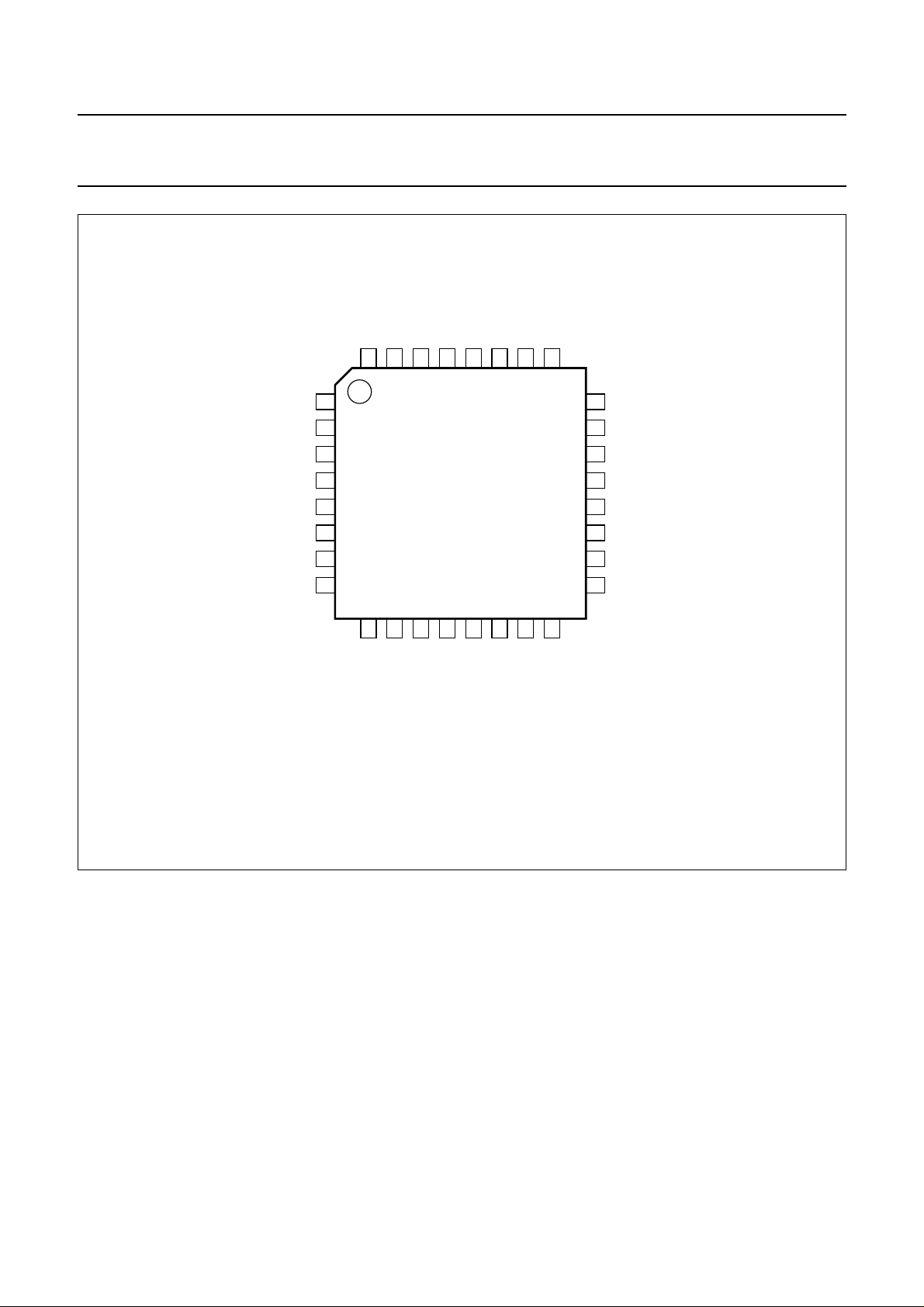
ORDERING INFORMATION
TYPE
NUMBER
TZA3000HL LQFP32 plastic low profile quad flat package; 32 leads; body 5 × 5 × 1.4 mm SOT401-1
TZA3000U naked die die in waffle pack carriers; die dimensions 1.58 × 1.58 mm −
NAME DESCRIPTION VERSION
APPLICATIONS
• Digital fibre optic receiver in short, medium and long
haul optical telecommunications transmission systems
or in high speed data networks
• Wideband RF gain block.
DESCRIPTION
The TZA3000 optical receiver is a low-noise
transimpedance amplifier with AGC plus a limiting
amplifier designed to be used in SDH/SONET fibre optic
links. The TZA3000 amplifies the current generated by a
photo detector (PIN diode or avalanche photodiode) and
converts it to a differential output voltage.
PACKAGE
1997 Oct 17 2
Page 3
Philips Semiconductors Objective specification
SDH/SONET STM4/OC12 optical receiver TZA3000
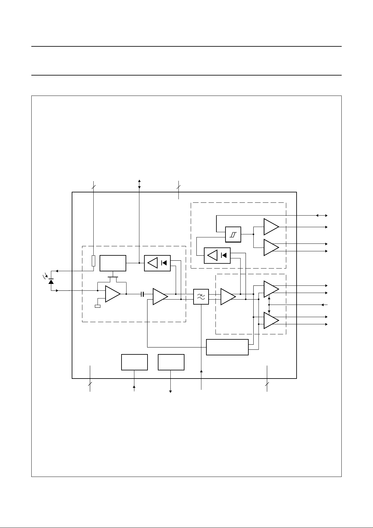
BLOCK DIAGRAM
handbook, full pagewidth
DREF
V
CCA
2
kΩ
4
7IPhoto
PREAMPLIFIER
AGC
2 2
2, 5 17, 2031
peak detector
GAIN-
CONTROL
V
CCD
A1 A2
LOS DETECTION
LIMITING
AMPLIFIER
DC-OFFSET
COMPENSATION
TTL
PECL
CML
PECL
29 LOSTH
LOSTTL
28
26 LOS
LOSQ
27
18 OUTCML
19 OUTQCML
OUTSEL
15
22 OUTPECL
OUTQPECL
23
BIASING
11
V
ref
AGND
1, 3, 6, 8
9, 30, 32
7
TESTING
14
RFTEST
Fig.1 Block diagram.
1997 Oct 17 3
BWC
TZA3000
10
DGND
13, 16, 21
24, 25
5
MGK881
Page 4

Philips Semiconductors Objective specification
SDH/SONET STM4/OC12 optical receiver TZA3000
PINNING
SYMBOL PIN TYPE DESCRIPTION
AGND 1 ground analog ground
V
CCA
AGND 3 ground analog ground
DREF 4 analog output bias voltage for PIN diode (V
V
CCA
AGND 6 ground analog ground
IPhoto 7 analog input current input; connect the anode of PIN diode to this pin; DC bias level is
AGND 8 ground analog ground
AGND 9 ground analog ground
BWC 10 analog input bandwidth control pin; default bandwidth is 470 MHz; a resistor should be
V
ref
SUB 12 substrate substrate pin; to be connected to AGND
DGND 13 ground digital ground
RFTEST 14 analog input test pin; not used in application; not connected
OUTSEL 15 CMOS input output select pin; when OUTSEL is HIGH, CML data outputs are active and
DGND 16 ground digital ground
V
CCD
OUTCML 18 CML output CML data output; OUTCML goes HIGH when current flows into IPhoto (pin 7)
OUTQCML 19 CML output CML compliment of OUTCML (pin 18)
V
CCD
DGND 21 ground digital ground
OUTPECL 22 PECL output PECL data output; OUTPECL goes HIGH when current flows into IPhoto (pin 7)
OUTQPECL 23 PECL output PECL compliment of OUTPECL (pin 22)
DGND 24 ground digital ground
DGND 25 ground digital ground
LOS 26 PECL output PECL-compatible LOS detection pin; LOS output is HIGH when the input signal
LOSQ 27 PECL output PECL compliment of LOS
LOSTTL 28 TTL output CMOS-compatible LOS detection pin; the LOSTTL output is HIGH when the
LOSTH 29 analog I/O pin for setting input threshold level; nominal DC voltage is V
AGND 30 ground analog ground
AGC 31 analog I/O AGC monitor voltage; the internal AGC circuit can be disabled by applying an
AGND 32 ground analog ground
2 supply analog supply voltage
); cathode should be connected to this pin
CCA
5 supply analog supply voltage
800 mV, one diode voltage above ground
connected between V
(pin 11) and BWC (pin 10) to decrease bandwidth, or
ref
between BWC (pin 10) and AGND to increase bandwidth
11 analog output band gap reference voltage; nominal value approximately 1.2 V
PECL data outputs are disabled; OUTSEL is pulled LOW if left unconnected,
PECL data outputs will then be active and CML data outputs disabled
17 supply digital supply voltage
20 supply digital supply voltage
is below the user programmable threshold level
input signal is below the user programmable threshold level
CCA
threshold level set by connecting an external resistor between LOSTH and
V
or by forcing a current into LOSTH; default value for this resistor is 86 kΩ
CCA
external voltage to this pin
− 1.5 V;
1997 Oct 17 4
Page 5
Philips Semiconductors Objective specification
SDH/SONET STM4/OC12 optical receiver TZA3000
handbook, full pagewidth
AGND
V
CCA
AGND
DREF
V
CCA
AGND
IPhoto
AGND
AGC
AGND
32
1
2
3
4
AGND
31
30
LOSTH
29
LOSTTL
28
TZA3000HL
5
6
7
8
9
AGND
10
BWC
11
12
13
ref
V
SUB
DGND
LOS
LOSQ
27
26
14
15
RFTEST
OUTSEL
DGND
25
16
DGND
DGND
24
OUTQPECL
23
OUTPECL
22
21
DGND
V
20
CCD
19
OUTQCML
18
OUTCML
V
17
CCD
MGK880
Fig.2 Pin configuration.
1997 Oct 17 5
Page 6
Philips Semiconductors Objective specification
SDH/SONET STM4/OC12 optical receiver TZA3000
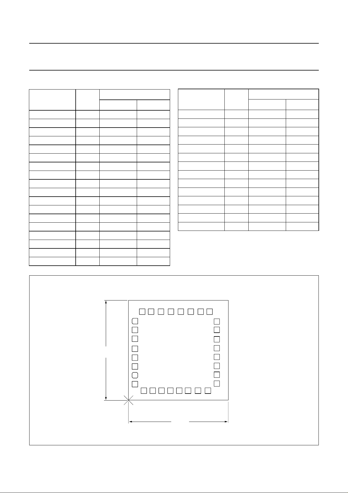
CHIP DIMENSIONS AND BONDING PAD LOCATIONS
COORDINATES
(1)
SYMBOL PAD
xy
AGND 1 102 1251
V
CCA
2 102 1111
AGND 3 102 971
DREF 4 102 814
V
CCA
5 102 674
AGND 6 102 534
IPhoto 7 102 395
AGND 8 102 254
AGND 9 243 105
BWC 10 383 105
V
ref
11 523 105
SUB 12 663 105
DGND 13 803 105
RFTEST 14 943 105
OUTSEL 15 1100 105
DGND 16 1257 105
V
CCD
17 1398 263
OUTCML 18 1398 403
SYMBOL PAD
COORDINATES
xy
OUTQCML 19 1398 543
V
CCD
20 1398 683
DGND 21 1398 823
OUTPECL 22 1398 963
OUTQPECL 23 1398 1103
DGND 24 1398 1243
DGND 25 1283 1400
LOS 26 1143 1400
LOSQ 27 986 1400
LOSTTL 28 829 1400
LOSTH 29 671 1400
AGND 30 514 1400
AGC 31 357 1400
AGND 32 217 1400
Note
1. All coordinates are referenced, in µm, to the bottom
left-hand corner of the die.
(1)
handbook, full pagewidth
AGND31AGC30AGND29LOSTH28LOSTTL27LOSQ26LOS25DGND
32
AGND 1
1.58
mm
V
AGND
DREF 4
V
AGND 6
IPhoto 7
AGND 8
x
CCA
CCA
2
3
TZA3000U
5
9
10
11
12
0
0
y
AGND
BWC
ref
V
Fig.3 Bonding pad locations: TZA3000U.
1997 Oct 17 6
13
SUB
1.58 mm
14
DGND
15
RFTEST
16
DGND
OUTSEL
DGND
24
OUTQPECL23
OUTPECL22
DGND21
V
20
17
CCD
OUTQCML19
OUTCML18
V
CCD
MGK882
Page 7

Philips Semiconductors Objective specification
SDH/SONET STM4/OC12 optical receiver TZA3000
FUNCTIONAL DESCRIPTION
The TZA3000 contains five functional blocks:
• Preamplifier input stage
• Low-pass filter
• Limiting amplifier stage
• Offset compensation loop
• Loss-of-signal detection unit.
Preamplifier
The preamplifier provides low-noise amplification of the
current generated by a photodiode connected to the
IPhoto pin.
A differential amplifier converts the output of the
preamplifier to a differential voltage. An AGC loop
increases the dynamic range of the receiver by reducing
the feedback resistance of the preamplifier. The AGC loop
hold capacitor is integrated on-chip, so an external
capacitor is not needed for AGC. The AGC voltage can be
monitored at pin 31. This pin can be left unconnected for
normal operation. It can also be used to force an external
AGC voltage. If pin 31 (AGC) is connected to AGND, the
internal AGC loop is disabled and the receiver gain is at a
maximum. In this case, the maximum input current is about
50 µA.
Low-pass filter
A low-pass filter controls the bandwidth of the receiver,
which can be varied between 300 and 600 MHz.
The bandwidth is set to 470 MHz by default. It can be
decreased by connecting a resistor between BWC (pin 10)
and V
(pin 11) or increased by connecting a resistor
ref
between BWC and AGND.
Limiting amplifier
A limiting amplifier boosts the signal up to PECL levels.
The output can be either CML or PECL compatible,
selected by means of pin OUTSEL. When OUTSEL is
HIGH, CML data outputs are active and PECL data
outputs are disabled. If OUTSEL is left unconnected, it is
pulled LOW and PECL data outputs are active while CML
data outputs are disabled.
Offset cancellation loop
A control loop connected between the limiting amplifier
output and the differential amplifier input cancels the DC
offset. The loop bandwidth is fixed internally at 30 kHz.
Loss-of-signal detection (LOS)
The LOS section detects an input signal level below a fixed
threshold. The threshold is determined by the current
through pin LOSTH. If this current is increased, the
threshold level will rise. An external resistor between
LOSTH and V
can be used, or a current can be forced
CCA
into LOSTH. The default value for the external resistor is
86 kΩ. In this case, the current through LOSTH will be
approximately 17.4 µA since the voltage at pin LOSTH is
regulated at 1.5 V below the supply voltage. This threshold
corresponds to an input current of 0.96 µA. The ratio of
LOSTH current to input current is thus approximately
18 : 1. When the input signal level falls below this
threshold, the LOS (PECL compatible) and LOSTTL (TTL
compatible) outputs go HIGH. The hysteresis is fixed
internally at 3 dB. Response time is typically less than
20 µs.
1997 Oct 17 7
Page 8

Philips Semiconductors Objective specification
SDH/SONET STM4/OC12 optical receiver TZA3000
LIMITING VALUES
In accordance with the Absolute Maximum Rating System (IEC 134).
SYMBOL PARAMETER MIN. MAX. UNIT
V
CC
V
n
I
n
P
tot
T
stg
T
j
T
amb
supply voltage −0.5 +6 V
DC voltage
pin 7: IPhoto −0.5 +1 V
pin 14: RFTEST −0.5 V
pins 22, 23, 26 and 27: OUTPECL, OUTQPECL, LOS and LOSQ V
pins 18 and 19: OUTCML and OUTQCML V
− 2VCC+ 0.5 V
CC
− 2VCC+ 0.5 V
CC
pin 29: LOSTH −0.5 V
+ 0.5 V
CC
+ 0.5 V
CC
pin 10: BWC −0.5 +3.2 V
pin 31: AGC −0.5 V
pin 11: V
ref
−0.5 +3.2 V
pin 4: DREF −0.5 V
pin 15: OUTSEL −0.5 V
pin 28: LOSTTL −0.5 V
+ 0.5 V
CC
+ 0.5 V
CC
+ 0.5 V
CC
+ 0.5 V
CC
DC current
pin 7: IPhoto −1 +2.5 mA
pin 14: RFTEST −2+2mA
pins 22, 23, 26 and 27: OUTPECL, OUTQPECL, LOS and LOSQ −25 +10 mA
pins 18,19: OUTCML and OUTQCML −15 +15 mA
pin 29: LOSTH −2+2mA
pin 10: BWC −1+1mA
pin 31: AGC −0.2 +0.2 mA
pin 11: V
ref
−2 +2.5 mA
pin 4: DREF −2.5 +2.5 mA
pin 15: OUTSEL −0.5 +0.5 mA
pin 28: LOSTTL −16 +16 mA
total power dissipation − 600 mW
storage temperature −65 +150 °C
junction temperature − 150 °C
ambient temperature −40 +85 °C
THERMAL CHARACTERISTICS
SYMBOL PARAMETER VALUE UNIT
R
R
th(j-s)
th(j-a)
thermal resistance from junction to solder point tbf K/W
thermal resistance from junction to ambient tbf K/W
1997 Oct 17 8
Page 9

Philips Semiconductors Objective specification
SDH/SONET STM4/OC12 optical receiver TZA3000
CHARACTERISTICS
For typical values T
temperature range and process spread.
SYMBOL PARAMETER CONDITIONS MIN. TYP. MAX. UNIT
V
I
CCD
I
CCA
P
T
T
R
CC
tot
j
amb
tr
supply voltage 3 5 5.5 V
digital supply current note 1 13 20 28 mA
analog supply current 24 36 51 mA
total power dissipation −−525 mW
junction temperature −40 − +110 °C
ambient temperature −40 +25 +85 °C
small-signal transresistance
of the receiver
f
−3dB(h)
f
−3dB(l)
I
i(IPhoto)(p-p)
high frequency −3dB point pin BWC left
low frequency −3dB point 20 30 40 kHz
input current on pin IPhoto
(peak-to-peak value)
V
bias(IPhoto)
input bias voltage on pin
IPhoto
I
n(tot)
total integrated RMS noise
current over bandwidth
(referenced to input)
PSRR power supply rejection ratio
at V
∆R
/∆t AGC loop constant − 1 − dB/ms
tr
PECL outputs: OUTPECL and OUTQPECL
V
OL
V
OH
V
OO
LOW-level output voltage 50 Ω to VCC− 2V VCC− 1100 − VCC− 900 mV
HIGH-level output voltage 50 Ω to VCC− 2V VCC− 1840 − VCC− 1620 mV
differential output offset
voltage
t
r
t
f
rise time 20% to 80% − 200 300 ps
fall time 80% to 20% − 140 250 ps
=25°C and VCC= 5 V; minimum and maximum values are valid over the entire ambient
amb
note 2 − 47 − mA
note 3 11 17 24 mA
measured differentially at
− 1800 − kΩ
PECL outputs
measured differentially at
− 1100 − kΩ
CML outputs
− 470 − MHz
unconnected; note 4
VCC=5V −400 +4 +1500 µA
V
= 3.3 V −400 +4 +500 µA
CC
720 800 970 mV
Ci= 1.2 pF; note 5
∆f = 311 MHz − 55 − nA
∆f = 450 MHz − 80 − nA
∆f = 622 MHz − 120 − nA
measured differentially;
CC
note 6
f = 100 kHz to 10 MHz − 12 µA/V
f = 10 MHz to 100 MHz − 25 µA/V
f = 100 MHz to 1 GHz − 5 100 µA/V
−10 − +10 mV
1997 Oct 17 9
Page 10

Philips Semiconductors Objective specification
SDH/SONET STM4/OC12 optical receiver TZA3000
SYMBOL PARAMETER CONDITIONS MIN. TYP. MAX. UNIT
PECL outputs: LOS and LOSQ
V
OL
V
OH
V
OO
t
r
t
f
CML outputs: OUTCML and OUTQCML
V
O
V
o(se)(p-p)
V
OO
R
o
t
r
t
f
LOW-level output voltage 50 Ω to VCC− 2V VCC− 1100 − VCC− 900 mV
HIGH-level output voltage 50 Ω to VCC− 2V VCC− 1840 − VCC− 1620 mV
differential output offset
−10 − +10 mV
voltage
rise time 20% to 80% −−600 ns
fall time 80% to 20% −−200 ns
single ended output voltage 50 Ω to V
single-ended output voltage
50 Ω to V
CC
CC
VCC− 260 − V
CC
mV
150 200 260 mV
(peak-to-peak value)
differential output offset
50 Ω to V
CC
−10 − +10 mV
voltage
single ended output
80 100 120 Ω
resistance
rise time 20% to 80%;
− 92 − ps
50 Ω, 1 pF load
fall time 80% to 20%;
− 62 − ps
50 Ω, 1 pF load
CMOS input: OUTSEL
V
IL
V
IH
LOW-level input voltage − 0.4 0.8 V
HIGH-level input voltage VCC− 1VCC− 0.5 − V
CMOS output: LOSTTL
V
OL
V
OH
LOW-level output voltage 0 − 0.2 V
HIGH-level output voltage VCC− 0.2 − V
CC
V
Notes
1. OUTPECL, OUTQPECL, OUTCML, OUTQCML, LOS and LOSQ outputs are left unconnected. OUTPECL and
OUTQPECL outputs are active.
2. OUTPECL and OUTQPECL outputs are terminated with 50 Ω to VT. VT is an external termination voltage for PECL
outputs and is 2 V below the supply voltage. OUTCML, OUTQCML, LOS and LOSQ outputs are left unconnected
3. OUTCML and OUTQCML outputs are terminated with 50 Ω to V
; CML outputs are active. OUTPECL,
CCD
OUTQPECL, LOS and LOSQ outputs are left unconnected
4. The bandwidth is set to 470 MHz by default. It can be varied between 300 and 600 MHz by adjusting the voltage at
pin BWC.
5. All I
measurements were made with an input capacitance of Ci= 1.2 pF. This was comprised of 0.7 pF for the
n(tot)
photodiode itself, with 0.3 pF allowed for the PCB layout and 0.2 pF intrinsic to the package.
6. PSRR is defined as the ratio of the equivalent current change at the input (∆I
∆I
PSRR
For example, a 1 mV disturbance on V
=
--------------------
IPhoto
∆V
CC
at 10 MHz will typically generate the equivalent of 2 nA extra photodiode
CC
) to a change in supply voltage:
IPhoto
current.
1997 Oct 17 10
Page 11

Philips Semiconductors Objective specification
SDH/SONET STM4/OC12 optical receiver TZA3000
APPLICATION INFORMATION
handbook, full pagewidth
DREF
IPhoto
22 nF
2
V
CCA
4
7
1, 3, 6, 8
9, 30, 32
AGND31AGC10BWC14RFTEST
7
Fig.4 Application diagram: PECL data outputs active.
86 kΩ
LOSTH
TZA3000
680 nF
17, 20292, 5
11
V
ref
V
CC
2
V
15
10 µH10 µH
CCD
OUTSEL
22 nF
13, 16, 21
24, 25
DGND
5
LOSQ
27
LOS
26
LOSTTL
28
OUTQPECL
23
OUTPECL
22
OUTQCML
19
OUTCML
18
Zo = 50 Ω
R1 R1
Zo = 50 Ω
R2 R2
MGK883
handbook, full pagewidth
DREF
IPhoto
22 nF
2
V
CCA
4
7
1, 3, 6, 8
9, 30, 32
AGND31AGC10BWC14RFTEST
7
Fig.5 Application diagram: CML data outputs active.
86 kΩ
LOSTH
TZA3000
680 nF
17, 20292, 5
11
V
ref
V
CC
2
V
15
10 µH10 µH
CCD
OUTSEL
22 nF
13, 16, 21
24, 25
DGND
5
LOSQ
27
LOS
26
LOSTTL
28
OUTQPECL
23
OUTPECL
22
OUTQCML
19
OUTCML
18
Zo = 50 Ω
Zo = 50 Ω
50Ω50
MGK884
Ω
1997 Oct 17 11
Page 12

Philips Semiconductors Objective specification
SDH/SONET STM4/OC12 optical receiver TZA3000
handbook, full pagewidth
CML/PECL OUTPUT
V
CC
V
O(max)
V
OQH
V
OH
V
o (p-p)
V
V
O(min)
OQL
V
OL
V
OO
MGK885
Fig.6 Logic level symbol definitions for CML and PECL.
handbook, full pagewidth
OUTCML OUTQCML
V
CC
100 Ω 100 Ω
6 mA
V
CC
a. CML. b. PECL.
Fig.7 Output circuits.
1997 Oct 17 12
105 Ω 105 Ω
9 mA
OUTPECL
OUTQPECL
0.5 mA
0.5 mA
MGK886
Page 13

Philips Semiconductors Objective specification
SDH/SONET STM4/OC12 optical receiver TZA3000
PECL outputs: OUTPECL (22), OUTQPECL (23), LOS (26) and LOSQ (27)
handbook, full pagewidth
VCC = 3.3 V
R1 = 127 Ω
V
V
IQ
V
I
V
IQ
V
I
OQ
V
O
R2 = 82.5 Ω
GND
VCC = 5 V
R1 = 83.3 Ω
V
OQ
V
O
R2 = 125 Ω
R1 = 127 Ω
R2 = 82.5 Ω
R1 = 83.3 Ω
R2 = 125 Ω
Fig.8 PECL termination schemes.
1997 Oct 17 13
GND
MGK887
Page 14

Philips Semiconductors Objective specification
SDH/SONET STM4/OC12 optical receiver TZA3000
CML outputs: OUTCML (18) and OUTQCML (19)
The output impedance of the CML output driver is 100 Ω
(see Figs 7 and 9), which doesn’t match the characteristic
impedance of the strip line. While this means that the
reflections of some incident edges will arrive at the driver
output on the PCB, this value was selected to reduce
power dissipation inside the IC. The parallel combination
of 100 Ω and 50 Ω (33 Ω) will generate a signal swing of
200 mV peak-to-peak (single sided) with a tail current of
6 mA. If the output impedance was 50 Ω rather than
handbook, full pagewidth
V
CC
100Ω100
Ω
generator
inside TZA3000
V
O
V
OQ
interconnect
100 Ω, an 8 mA tail current would be needed to generate
the same voltage swing. This would increase power
dissipation by 33%.
If necessary, the output impedance of the generator can
be matched to the line impedance by connecting an
external 100 Ω resistor in parallel with the output as shown
in Fig.10. The magnitude of the output voltage swing will
not change due to adaptive regulation. However, power
dissipation will increase by 33%.
PCB
Zo = 50 Ω
Zo = 50 Ω
V
I
V
IQ
receiver
inside TZA3004
V
CC
50 Ω
50 Ω
handbook, full pagewidth
Fig.9 CML interface circuit without matched impedance; low power dissipation.
V
CC
100Ω100
Ω
generator
inside TZA3000
V
O
V
OQ
interconnect
100Ω100
Ω
PCB
Zo = 50 Ω
Zo = 50 Ω
receiver
inside TZA3004
V
V
50 Ω
I
50 Ω
IQ
Fig.10 CML interface circuit with matched impedance; higher power dissipation.
MGK888
V
CC
MGK889
1997 Oct 17 14
Page 15

Philips Semiconductors Objective specification
SDH/SONET STM4/OC12 optical receiver TZA3000
PACKAGE OUTLINE
LQFP32: plastic low profile quad flat package; 32 leads; body 5 x 5 x 1.4 mm
c
y
X
A
H
E
E
A
2
A
A
25
32
24
17
Z
16
E
e
b
w M
p
pin 1 index
9
1
8
SOT401-1
(A )
1
L
L
detail X
3
θ
p
Z
e
w M
b
p
D
H
D
D
B
v M
v M
0 2.5 5 mm
scale
DIMENSIONS (mm are the original dimensions)
UNIT
mm
A
max.
1.60
A
1A2A3bp
0.15
1.5
1.3
0.25
0.05
cE
0.27
0.18
0.17
0.12
(1)
(1) (1)(1)
D
5.1
4.9
eH
H
5.1
4.9
0.5
7.15
6.85
Note
1. Plastic or metal protrusions of 0.25 mm maximum per side are not included.
OUTLINE
VERSION
IEC JEDEC EIAJ
REFERENCES
SOT401-1
1997 Oct 17 15
D
A
B
E
7.15
6.85
LL
p
0.75
1.0
0.45
0.2
0.12 0.1
EUROPEAN
PROJECTION
Z
0.95
0.55
D
Zywv θ
E
0.95
0.55
o
7
o
0
ISSUE DATE
95-12-19
97-08-04
Page 16

Philips Semiconductors Objective specification
SDH/SONET STM4/OC12 optical receiver TZA3000
SOLDERING
Introduction
There is no soldering method that is ideal for all IC
packages. Wave soldering is often preferred when
through-hole and surface mounted components are mixed
on one printed-circuit board. However, wave soldering is
not always suitable for surface mounted ICs, or for
printed-circuits with high population densities. In these
situations reflow soldering is often used.
This text gives a very brief insight to a complex technology.
A more in-depth account of soldering ICs can be found in
our
“IC Package Databook”
Reflow soldering
Reflow soldering techniques are suitable for all LQFP
packages.
Reflow soldering requires solder paste (a suspension of
fine solder particles, flux and binding agent) to be applied
to the printed-circuit board by screen printing, stencilling or
pressure-syringe dispensing before package placement.
Several techniques exist for reflowing; for example,
thermal conduction by heated belt. Dwell times vary
between 50 and 300 seconds depending on heating
method. Typical reflow temperatures range from
215 to 250 °C.
Preheating is necessary to dry the paste and evaporate
the binding agent. Preheating duration: 45 minutes at
45 °C.
Wave soldering
Wave soldering is not recommended for LQFP packages.
This is because of the likelihood of solder bridging due to
closely-spaced leads and the possibility of incomplete
solder penetration in multi-lead devices.
(order code 9398 652 90011).
If wave soldering cannot be avoided, the following
conditions must be observed:
• A double-wave (a turbulent wave with high upward
pressure followed by a smooth laminar wave)
soldering technique should be used.
• The footprint must be at an angle of 45° to the board
direction and must incorporate solder thieves
downstream and at the side corners.
Even with these conditions, do not consider wave
soldering LQFP packages LQFP48 (SOT313-2),
LQFP64 (SOT314-2) or LQFP80 (SOT315-1).
During placement and before soldering, the package must
be fixed with a droplet of adhesive. The adhesive can be
applied by screen printing, pin transfer or syringe
dispensing. The package can be soldered after the
adhesive is cured.
Maximum permissible solder temperature is 260 °C, and
maximum duration of package immersion in solder is
10 seconds, if cooled to less than 150 °C within
6 seconds. Typical dwell time is 4 seconds at 250 °C.
A mildly-activated flux will eliminate the need for removal
of corrosive residues in most applications.
Repairing soldered joints
Fix the component by first soldering two diagonallyopposite end leads. Use only a low voltage soldering iron
(less than 24 V) applied to the flat part of the lead. Contact
time must be limited to 10 seconds at up to 300 °C. When
using a dedicated tool, all other leads can be soldered in
one operation within 2 to 5 seconds between
270 and 320 °C.
1997 Oct 17 16
Page 17

Philips Semiconductors Objective specification
SDH/SONET STM4/OC12 optical receiver TZA3000
DEFINITIONS
Data sheet status
Objective specification This data sheet contains target or goal specifications for product development.
Preliminary specification This data sheet contains preliminary data; supplementary data may be published later.
Product specification This data sheet contains final product specifications.
Limiting values
Limiting values given are in accordance with the Absolute Maximum Rating System (IEC 134). Stress above one or
more of the limiting values may cause permanent damage to the device. These are stress ratings only and operation
of the device at these or at any other conditions above those given in the Characteristics sections of the specification
is not implied. Exposure to limiting values for extended periods may affect device reliability.
Application information
Where application information is given, it is advisory and does not form part of the specification.
LIFE SUPPORT APPLICATIONS
These products are not designed for use in life support appliances, devices, or systems where malfunction of these
products can reasonably be expected to result in personal injury. Philips customers using or selling these products for
use in such applications do so at their own risk and agree to fully indemnify Philips for any damages resulting from such
improper use or sale.
1997 Oct 17 17
Page 18

Philips Semiconductors Objective specification
SDH/SONET STM4/OC12 optical receiver TZA3000
NOTES
1997 Oct 17 18
Page 19

Philips Semiconductors Objective specification
SDH/SONET STM4/OC12 optical receiver TZA3000
NOTES
1997 Oct 17 19
Page 20

Philips Semiconductors – a worldwide company
Argentina: see South America
Australia: 34 Waterloo Road, NORTH RYDE, NSW 2113,
Tel. +61 2 9805 4455, Fax. +61 2 9805 4466
Austria: Computerstr. 6, A-1101 WIEN, P.O. Box 213, Tel. +43 160 1010,
Fax. +43 160 101 1210
Belarus: Hotel Minsk Business Center, Bld. 3, r. 1211, Volodarski Str. 6,
220050 MINSK, Tel. +375 172 200 733, Fax. +375 172 200 773
Belgium: see The Netherlands
Brazil: seeSouth America
Bulgaria: Philips Bulgaria Ltd., Energoproject, 15thfloor,
51 James Bourchier Blvd., 1407 SOFIA,
Tel. +359 2 689 211, Fax. +359 2 689 102
Canada: PHILIPS SEMICONDUCTORS/COMPONENTS,
Tel. +1 800 234 7381
China/Hong Kong: 501 Hong Kong Industrial Technology Centre,
72 Tat Chee Avenue, Kowloon Tong, HONG KONG,
Tel. +852 2319 7888, Fax. +852 2319 7700
Colombia: see South America
Czech Republic: see Austria
Denmark: Prags Boulevard 80, PB 1919, DK-2300 COPENHAGEN S,
Tel. +45 32 88 2636, Fax. +45 31 57 0044
Finland: Sinikalliontie 3, FIN-02630 ESPOO,
Tel. +358 9 615800, Fax. +358 9 61580920
France: 4 Rue du Port-aux-Vins, BP317, 92156 SURESNES Cedex,
Tel. +33 1 40 99 6161, Fax. +33 1 40 99 6427
Germany: Hammerbrookstraße 69, D-20097 HAMBURG,
Tel. +49 40 23 53 60, Fax. +49 40 23 536 300
Greece: No. 15, 25th March Street, GR 17778 TAVROS/ATHENS,
Tel. +30 1 4894 339/239, Fax. +30 1 4814 240
Hungary: seeAustria
India: Philips INDIA Ltd, Band Box Building, 2nd floor,
254-D, Dr. Annie Besant Road, Worli, MUMBAI 400 025,
Tel. +91 22 493 8541, Fax. +91 22 493 0966
Indonesia: see Singapore
Ireland: Newstead, Clonskeagh, DUBLIN 14,
Tel. +353 1 7640 000, Fax. +353 1 7640 200
Israel: RAPAC Electronics, 7 Kehilat Saloniki St, PO Box 18053,
TEL AVIV 61180, Tel. +972 3 645 0444, Fax. +972 3 649 1007
Italy: PHILIPS SEMICONDUCTORS, Piazza IV Novembre 3,
20124 MILANO, Tel. +39 2 6752 2531, Fax. +39 2 6752 2557
Japan: Philips Bldg 13-37, Kohnan 2-chome, Minato-ku, TOKYO 108,
Tel. +81 3 3740 5130, Fax. +81 3 3740 5077
Korea: Philips House, 260-199 Itaewon-dong, Yongsan-ku, SEOUL,
Tel. +82 2 709 1412, Fax. +82 2 709 1415
Malaysia: No. 76 Jalan Universiti, 46200 PETALING JAYA, SELANGOR,
Tel. +60 3 750 5214, Fax. +60 3 757 4880
Mexico: 5900 Gateway East, Suite 200, EL PASO, TEXAS 79905,
Tel. +9-5 800 234 7381
Middle East: see Italy
Netherlands: Postbus 90050, 5600PB EINDHOVEN, Bldg. VB,
Tel. +3140 27 82785, Fax. +31 40 27 88399
New Zealand: 2 Wagener Place, C.P.O. Box 1041, AUCKLAND,
Tel. +64 9 849 4160, Fax. +64 9 849 7811
Norway: Box 1, Manglerud 0612, OSLO,
Tel. +47 22 74 8000, Fax. +47 22 74 8341
Philippines: Philips Semiconductors Philippines Inc.,
106 Valero St. Salcedo Village, P.O. Box 2108 MCC, MAKATI,
Metro MANILA, Tel. +63 2 816 6380, Fax. +63 2 817 3474
Poland: Ul. Lukiska 10, PL 04-123 WARSZAWA,
Tel. +48 22 612 2831, Fax. +48 22 612 2327
Portugal: see Spain
Romania: see Italy
Russia: Philips Russia, Ul. Usatcheva 35A, 119048 MOSCOW,
Tel. +7 095 755 6918, Fax. +7 095 755 6919
Singapore: Lorong 1, Toa Payoh, SINGAPORE 1231,
Tel. +65 350 2538, Fax. +65 251 6500
Slovakia: see Austria
Slovenia: see Italy
South Africa: S.A. PHILIPS Pty Ltd., 195-215 Main Road Martindale,
2092 JOHANNESBURG, P.O. Box 7430 Johannesburg 2000,
Tel. +27 11 470 5911, Fax. +27 11 470 5494
South America: Rua do Rocio 220, 5th floor, Suite 51,
04552-903 São Paulo, SÃO PAULO - SP, Brazil,
Tel. +55 11 821 2333, Fax. +55 11 829 1849
Spain: Balmes 22, 08007 BARCELONA,
Tel. +34 3 301 6312, Fax. +34 3 301 4107
Sweden: Kottbygatan 7, Akalla, S-16485 STOCKHOLM,
Tel. +46 8 632 2000, Fax. +46 8 632 2745
Switzerland: Allmendstrasse 140, CH-8027 ZÜRICH,
Tel. +41 1 488 2686, Fax. +41 1 481 7730
Taiwan: Philips Semiconductors, 6F, No. 96, Chien Kuo N. Rd., Sec. 1,
TAIPEI, Taiwan Tel. +886 2 2134 2865, Fax. +886 2 2134 2874
Thailand: PHILIPS ELECTRONICS (THAILAND) Ltd.,
209/2 Sanpavuth-Bangna Road Prakanong, BANGKOK 10260,
Tel. +66 2 745 4090, Fax. +66 2 398 0793
Turkey: Talatpasa Cad. No. 5, 80640 GÜLTEPE/ISTANBUL,
Tel. +90 212 279 2770, Fax. +90 212 282 6707
Ukraine: PHILIPS UKRAINE, 4 Patrice Lumumba str., Building B, Floor 7,
252042 KIEV, Tel. +380 44 264 2776, Fax. +380 44 268 0461
United Kingdom: Philips Semiconductors Ltd., 276 Bath Road, Hayes,
MIDDLESEX UB3 5BX, Tel. +44 181 730 5000, Fax. +44 181 754 8421
United States: 811 East Arques Avenue, SUNNYVALE, CA 94088-3409,
Tel. +1 800 234 7381
Uruguay: see South America
Vietnam: see Singapore
Yugoslavia: PHILIPS, Trg N. Pasica 5/v, 11000 BEOGRAD,
Tel. +381 11 625 344, Fax.+381 11 635 777
For all other countries apply to: Philips Semiconductors, Marketing & Sales Communications,
Building BE-p, P.O. Box 218, 5600 MD EINDHOVEN, The Netherlands, Fax. +31 40 27 24825
© Philips Electronics N.V. 1997 SCA55
All rights are reserved. Reproduction in whole or in part is prohibited without the prior written consent of the copyright owner.
The information presented in this document does not form part of any quotation or contract, is believed to be accurate and reliable and may be changed
without notice. No liability will be accepted by the publisher for any consequence of its use. Publication thereof does not convey nor imply any license
under patent- or other industrial or intellectual property rights.
Internet: http://www.semiconductors.philips.com
Printed in The Netherlands 427027/300/01/pp20 Date of release: 1997Oct 17 Document order number: 9397 750 01679
 Loading...