

Page 1
DATA SH EET
Preliminary specification
File under Integrated Circuits, IC01
1999 Sep 17
INTEGRATED CIRCUITS
TZA1027
Analog current buffer for CD-R and
CD-RW systems
Page 2
1999 Sep 17 2
Philips Semiconductors Preliminary specification
Analog current buffer for CD-R and CD-RW
systems
TZA1027
FEATURES
• Eight amplifiers for servo and power calibration
functions
• Gain selector for CD-R and CD-RW discs
• Separate dataamplifier for read speed up to thirty times
nominal data speed.
GENERAL DESCRIPTION
The TZA1027 is an analog current buffer IC for CD-R and
CD-RW systems with a 3-spot push-pull tracking system.
The IC interfaces directly to the photo diodes and
TZA1020. A HF current amplifier is implemented to detect
the actual HF data signal.
QUICK REFERENCE DATA
ORDERING INFORMATION
SYMBOL PARAMETER CONDITIONS MIN. TYP. MAX. UNIT
V
DD
supply voltage 4.5 5.0 5.5 V
I
i(cd)
central diode input current WRON = 1 0 − 3400 µA
I
i(sd)
satellite diode input current WRON = 1 0 − 520 µA
B
CAHF
bandwidth Ci= 5 pF 72 −−MHz
t
d(f)
flatness delay Ci= 5 pF; f = 0.1 to 32 MHz − 30 200 ps
G
SS
servo satellite detector gain HG = 1 − 32 −
HG=0 − 8 −
T
amb
ambient temperature 0 − 70 °C
TYPE
NUMBER
PACKAGE
NAME DESCRIPTION VERSION
TZA1027HL LQFP32 plastic low profile quad flat package; 32 leads; body 5 × 5 × 1.4 mm SOT401-1
Page 3
1999 Sep 17 3
Philips Semiconductors Preliminary specification
Analog current bufferforCD-R and CD-RW
systems
TZA1027
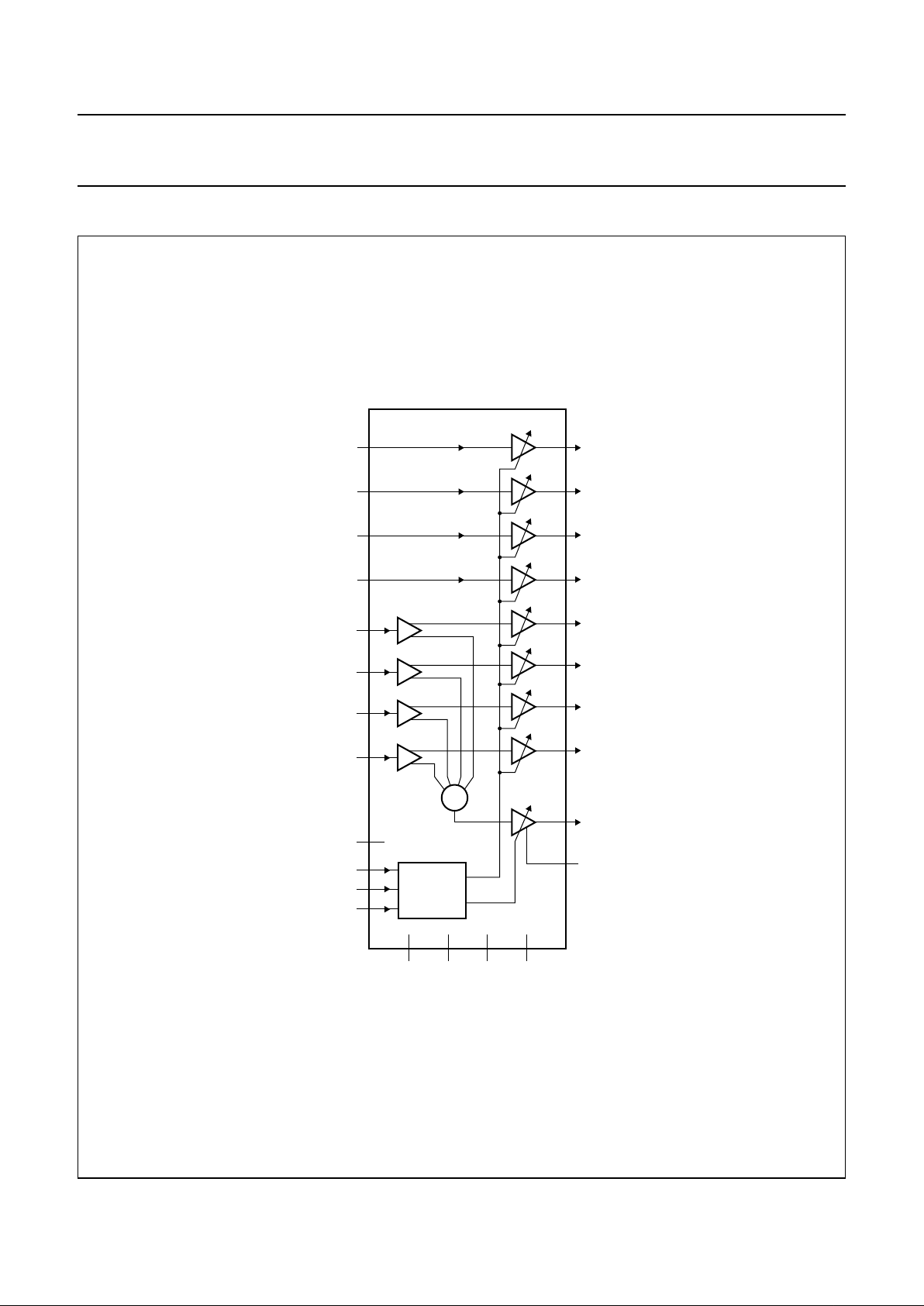
BLOCK DIAGRAM
Fig.1 Block diagram.
MGR881
handbook, full pagewidth
TZA1027
237
282
246
273
29
1
22
8
25
5
26
CAHF
C4LF
19
HFGND
18
4
C4
C3
C3LF
C2
C2LF
C1
C1LF
B2
B2LF
B1
B1LF
A2
A2LF
A1
A1LF
9, 10, 11, 12,
17, 20, 32
21
PDWN
31
WRON
30
HG
16
n.c.
+
15 13 14
AGND
V
DDD
V
DDA
GAIN
SELECTOR
DGND
Page 4

1999 Sep 17 4
Philips Semiconductors Preliminary specification
Analog current bufferforCD-R and CD-RW
systems
TZA1027
PINNING
SYMBOL PIN DESCRIPTION
C1 1 central photo diode current input
A2 2 satellite diode current input
B2 3 satellite diode current input
C4 4 central photo diode current input
C3 5 central photo diode current input
B1 6 satellite diode current input
A1 7 satellite diode current input
C2 8 central photo diode current input
n.c. 9 not connected
n.c. 10 not connected
n.c. 11 not connected
n.c. 12 not connected
AGND 13 analog ground
DGND 14 digital ground
V
DDD
15 digital power supply
V
DDA
16 analog power supply
n.c. 17 not connected
HFGND 18 ground connection of CAHF output stage
CAHF 19 central aperture high-frequency output
n.c. 20 not connected
PDWN 21 digital input power-down
C2LF 22 C2 central detector signal output
A1LF 23 A1 satellite detector signal output
B1LF 24 B1 satellite detector signal output
C3LF 25 C3 central detector signal output
C4LF 26 C4 central detector signal output
B2LF 27 B2 satellite detector signal output
A2LF 28 A2 satellite detector signal output
C1LF 29 C1 central detector signal output
HG 30 digital input high gain selection
WRON 31 digital input write on gain selection
n.c. 32 not connected
Page 5
1999 Sep 17 5
Philips Semiconductors Preliminary specification
Analog current bufferforCD-R and CD-RW
systems
TZA1027
handbook, full pagewidth
TZA1027HL
MGR882
1
2
3
4
5
6
7
8
24
23
22
21
20
19
18
17
9
10
11
12
13
14
15
16
32
31
30
29
28
27
26
25
C1
C3
C2
A1
B2
B1
n.c.
n.c.
AGND
n.c.
V
DDD
C4LF
A2LF
n.c.
C1LF
C2LF
n.c.
B2LF
A1LF
n.c.
HFGND
PDWN
WRON
HG
V
DDA
C3LF
B1LF
CAHF
DGND
n.c.
C4
A2
Fig.2 Pin configuration.
Page 6

1999 Sep 17 6
Philips Semiconductors Preliminary specification
Analog current bufferforCD-R and CD-RW
systems
TZA1027
FUNCTIONAL DESCRIPTION
All detector signals are applied to wide-band amplifiers for servo and laser power calibration functions of the TZA1020.
Signals from the central detector are added and amplified to suitable levels for the decoder circuit. Current gain can be
selected for CD-R and CD-RW discs.
LIMITING VALUES
In accordance with the Absolute Maximum Rating System (IEC 134).
THERMAL CHARACTERISTICS
LOGIC FUNCTIONS
Note
1. X = don’t care.
SYMBOL PARAMETERS MIN. MAX. UNIT
V
DD
supply voltage 0 5.5 V
T
stg
storage temperature −6.5 +150 °C
T
amb
ambient temperature 0 70 °C
V
es
electrostatic handling:
Machine model −100 +100 V
Human body model −500 +500 V
SYMBOL PARAMETER CONDITION VALUE UNIT
R
th(j-a)
thermal resistance from junction to
ambient
in free air 95 K/W
PDWN WRON HG MODE
1 X; note 1 X; note 1 power-down
0 0 0 CD-R read
0 0 1 CD-RW read
0 1 0 CD-R write
0 1 1 CD-RW write
Page 7

1999 Sep 17 7
Philips Semiconductors Preliminary specification
Analog current bufferforCD-R and CD-RW
systems
TZA1027
CHARACTERISTICS
V
DDA=VDDD
=5V; T
amb
=25°C; I
i(cd)
=25µA with x = 1LF to 4LF; I
i(sd)
=4µA with y = A or B and z = 1LF or 2LF;
PDWN = 0; WRON = 0; HG = 0 and C
cd=Csd
= 5 pF; the given maximum and minimum values are 4σvalues; unless
otherwise specified. Signals available on the IC pins are upper case. Signals not visible on the IC pins are lower case.
SYMBOL PARAMETERS CONDITIONS MIN. TYP. MAX. UNIT
Supplies
V
DDA
analog supply voltage 4.5 5.0 5.5 V
V
DDD
digital supply voltage 4.5 5.0 5.5 V
∆V
DD
difference between
V
DDA
and V
DDD
−0.3 − +0.3 V
I
DDA
analog supply current PDWN = 1 − 0.1 − mA
− 13 − mA
I
DDD
digital supply current PDWN = 1 − 0 − mA
− 14 − mA
Detector inputs
I
NPUT CURRENT RANGE
I
i(cd)
central diode input current 1.0 − 75 µA
WRON = 1 0 − 3400 µA
I
i(sd)
satellite diode input current 0.6 − 9 µA
WRON = 1 0 − 520 µA
I
NPUT VOLTAGE LEVEL
V
i(cd)
central diode input voltage level 2.5 2.9 3.3 V
WRON = 1 2.6 3.0 3.4 V
V
i(sd)
satellite diode input voltage level 1.6 1.9 2.2 V
WRON = 1 1.7 2.0 2.3 V
I
NPUT RESISTANCE
R
i(cd)
central diode input resistance − 420 −Ω
WRON = 1; I
i(cd)
=1mA − 220 −Ω
R
i(sd)
satellite diode input resistance − 620 −Ω
WRON = 1; I
i(cd)
= 200 µA − 370 −Ω
Transfer functions
SERVO OUTPUTS CD
G
cd
servo central detector gain −0.93 −1 −1.07
HG = 1 −2.8 −3 −3.2
WRON = 1 −0.94 −1 −1.06
WRON = 1; HG = 1 −0.93 −1 −1.07
G
mm
gain mismatch 3σ−−3%
B
cd
bandwidth 33 44 − MHz
HG = 1; I
i(cd)
=6µA1822−MHz
WRON = 1; I
i(cd)
= 1000 µA 150 230 − MHz
WRON = 1; HG = 1; I
i(cd)
= 250 µA 100 130 − MHz
Page 8

1999 Sep 17 8
Philips Semiconductors Preliminary specification
Analog current bufferforCD-R and CD-RW
systems
TZA1027
Note
1. X = don’t care.
t
r
rise time WRON = 1; 30 µA<I
i(cd)
< 520 µA − 2 − ns
t
d
delay time WRON = 1;
30 µA<I
i(cd)
< 520 µA
− 2.5 − ns
SERVO OUTPUTS SD
G
SS
servo satellite detector gain HG = 1 −2.85 −3.05 −3.25
WRON = 0; HG = 0 −0.96 −1.02 −1.08
WRON = 1; HG = 0 −0.88 −0.95 −1.02
WRON = 1; HG = 1 −0.88 −0.95 −1.02
B
S
bandwidth HG = 1; I
i(cd)
=1µA24−− MHz
WRON = X; note 1; HG = X; note 1 46 −− MHz
t
r
rise time WRON = 1; 4 µA<I
i(cd)
<65 µA − 3.6 − ns
t
d
delay time WRON = 1; 4 µA<I
i(cd)
<65 µA − 4.5 − ns
DATA OUTPUT; PIN CAHF
G
SS
servo satellite detector gain 7.5 8.1 8.7
HG = 1 29 32 35
WRON = 1; HG = X; note 1 − 0 −
B
CAHF
bandwidth 80 −− MHz
HG = 1; I
i(cd)
=6µA72−− MHz
t
d(f)
flatness delay − 30 200 ps
HG = 1; I
i(cd)
=6µA − 170 − ps
I
n
noise current − 1.4 −µA
HG = 1; I
i(cd)
=6µA − 2 −µA
Output pins
V
o(cd)
central diode output voltage −0.2 − V
DDD
− 1V
V
o(sd)
satellite diode output voltage −0.2 − V
DDD
− 1V
V
o(CAHF)
data output voltage 1 − V
DDD
+ 0.2 V
R
o(cd)
central diode output resistance − 1 − MΩ
R
o(sd)
satellite diode output resistance − 5 − MΩ
R
CAHF
data output resistance − 40 − kΩ
Digital control signals
INPUT VOLTAGE LEVELS; PINS PDWN, WRON AND HG
V
IL
LOW-level input voltage −0.2 − +1.2 V
V
IH
HIGH-level input voltage 1.8 − V
DDD
+ 0.2 V
INPUT CURRENT
I
LI
input leakage current −1 − +1 µA
DELAY TIME
t
d
delay time − 0.3 −µs
SYMBOL PARAMETERS CONDITIONS MIN. TYP. MAX. UNIT
Page 9

1999 Sep 17 9
Philips Semiconductors Preliminary specification
Analog current bufferforCD-R and CD-RW
systems
TZA1027
TEST AND APPLICATION INFORMATION
MGR883
handbook, full pagewidth
4.7 kΩ
50 Ω
100 nF
50
Ω
3.9
pF
3.3 kΩ
50
Ω
470 kΩ
100 nF
3.9
pF
3.3 kΩ
470 kΩ
100 nF
3.9
pF
3.3 kΩ
470 kΩ
100 nF
3.9
pF
3.3 kΩ
470 kΩ
100 nF
3.9
pF
3.3 kΩ
470 kΩ
100 nF
3.9
pF
3.3 kΩ
470 kΩ
100 nF
3.9
pF
3.3 kΩ
470 kΩ
100 nF
3.9
pF
3.3 kΩ
470 kΩ
100 nF
4.7 kΩ
50 Ω
100 nF
4.7 kΩ
50 Ω
100 nF
4.7 kΩ
50 Ω
100 nF
4.7 kΩ
50 Ω
100 nF
4.7 kΩ
50 Ω
100 nF
4.7 kΩ
50 Ω
100 nF
4.7 kΩ
50 Ω
100 nF
1 kΩ
50 Ω
100 nF
GAIN
SELECTOR
TZA1027
237
282
246
273
29
1
22
8
25
5
26
CAHF
+5 V
+5 V
C4LF
19
HFGND
18
4
C4
C3
C3LF
C2
C2LF
C1
C1LF
B2
B2LF
B1
B1LF
A2
A2LF
A1
A1LF
21
PDWN
31
WRON
30
HG
16
+
15 13 14
V
bias(cd)
V
bias(sd)
I
i(sd)(AC)
I
i(cd)(AC)
+5 V
AGND
V
DDD
V
DDA
DGND
Fig.3 Test diagram.
Page 10

1999 Sep 17 10
Philips Semiconductors Preliminary specification
Analog current bufferforCD-R and CD-RW
systems
TZA1027
handbook, full pagewidth
MGR884
TZA1027
TZA1020
237
282
246
273
29
1
22
8
25
5
26
4
8
5
9
10
3
6
7
CAHF
C4LF
19
HFGND
to block
decoder/
encoder
GAIN
SELECTOR
18
4
C4
C3
C3LF
C2
C2LF
C1
C1LF
B2
B2LF
B1
B1LF
A2
A2LF
A1
A1LF
C4
C3
C2
C1
SB2
SB1
SA2
SA1
21
PDWN
31
WRON
30
HG
+
16 15 13 14
+5 V
+12 V
AGND
V
DDD
V
DDA
DGND
SAA7399
SAA7392
Fig.4 Application diagram.
Page 11

1999 Sep 17 11
Philips Semiconductors Preliminary specification
Analog current bufferforCD-R and CD-RW
systems
TZA1027
PACKAGE OUTLINE
0.2
UNIT
A
max.
A
1A2A3bp
cE
(1)
eH
E
LL
p
Zywv θ
REFERENCES
OUTLINE
VERSION
EUROPEAN
PROJECTION
ISSUE DATE
IEC JEDEC EIAJ
mm
1.60
0.15
0.05
1.5
1.3
0.25
0.27
0.17
0.18
0.12
5.1
4.9
0.5
7.15
6.85
1.0
0.95
0.55
7
0
o
o
0.12 0.1
DIMENSIONS (mm are the original dimensions)
Note
1. Plastic or metal protrusions of 0.25 mm maximum per side are not included.
0.75
0.45
SOT401-1
95-12-19
97-08-04
D
(1) (1)(1)
5.1
4.9
H
D
7.15
6.85
E
Z
0.95
0.55
D
b
p
e
E
B
8
D
H
b
p
E
H
v M
B
D
Z
D
A
Z
E
e
v M
A
X
1
32
25
24
17
16
9
θ
A
1
A
L
p
detail X
L
(A )
3
A
2
y
w M
w M
0 2.5 5 mm
scale
LQFP32: plastic low profile quad flat package; 32 leads; body 5 x 5 x 1.4 mm
SOT401-1
c
pin 1 index
Page 12

1999 Sep 17 12
Philips Semiconductors Preliminary specification
Analog current bufferforCD-R and CD-RW
systems
TZA1027
SOLDERING
Introduction to soldering surface mount packages
Thistextgives a very brief insight to a complextechnology.
A more in-depth account of soldering ICs can be found in
our
“Data Handbook IC26; Integrated Circuit Packages”
(document order number 9398 652 90011).
There is no soldering method that is ideal for all surface
mount IC packages. Wavesoldering is notalways suitable
for surface mount ICs, or for printed-circuit boards with
high population densities. In these situations reflow
soldering is often used.
Reflow soldering
Reflow soldering requires solder paste (a suspension of
fine solder particles, flux and binding agent) to be applied
tothe printed-circuit board by screenprinting,stencilling or
pressure-syringe dispensing before package placement.
Several methods exist for reflowing; for example,
infrared/convection heating in a conveyor type oven.
Throughput times (preheating, soldering and cooling)vary
between 100 and 200 seconds depending on heating
method.
Typical reflow peak temperatures range from
215 to 250 °C. The top-surface temperature of the
packages should preferable be kept below 230 °C.
Wave soldering
Conventional single wave soldering is not recommended
forsurfacemountdevices (SMDs) or printed-circuit boards
with a high component density, as solder bridging and
non-wetting can present major problems.
To overcome these problems the double-wave soldering
method was specifically developed.
If wave soldering is used the following conditions must be
observed for optimal results:
• Use a double-wave soldering method comprising a
turbulent wave with high upward pressure followed by a
smooth laminar wave.
• Forpackageswithleadson four sides, the footprint must
be placed at a 45° angle to the transport direction of the
printed-circuit board. The footprint must incorporate
solder thieves downstream and at the side corners.
• For packages with leads on two sides and a pitch (e):
– larger than or equal to 1.27 mm, the footprint
longitudinal axis is preferred to be parallel to the
transport direction of the printed-circuit board;
– smaller than 1.27 mm, the footprint longitudinal axis
must be parallel to the transport direction of the
printed-circuit board.
The footprint must incorporate solder thieves at the
downstream end.
During placement and before soldering, thepackage must
be fixed with a droplet of adhesive. The adhesive can be
applied by screen printing, pin transfer or syringe
dispensing. The package can be soldered after the
adhesive is cured.
Typical dwell time is 4 seconds at 250 °C. A
mildly-activated flux will eliminate the need for removal of
corrosive residues in most applications.
Manual soldering
Fix the component by first soldering two
diagonally-opposite end leads. Use a low voltage (24 V or
less) soldering iron applied to the flat part of the lead.
Contact time must be limited to 10 seconds at up to
300 °C.
When using a dedicated tool, all other leads can be
soldered in one operation within 2 to 5 seconds between
270 and 320 °C.
Page 13

1999 Sep 17 13
Philips Semiconductors Preliminary specification
Analog current bufferforCD-R and CD-RW
systems
TZA1027
Suitability of surface mount IC packages for wave and reflow soldering methods
Notes
1. All surface mount (SMD) packages are moisture sensitive. Depending upon the moisture content, the maximum
temperature (with respect to time) and body size of the package, there is a risk that internal or external package
cracks may occur due to vaporization of the moisture in them (the so called popcorn effect). For details, refer to the
Drypack information in the
“Data Handbook IC26; Integrated Circuit Packages; Section: Packing Methods”
.
2. These packages are not suitable for wave soldering as a solder joint between the printed-circuit board and heatsink
(at bottom version) can not be achieved, and as solder may stick to the heatsink (on top version).
3. If wave soldering is considered, then the package must be placed at a 45° angle to the solder wave direction.
The package footprint must incorporate solder thieves downstream and at the side corners.
4. Wave soldering is only suitable for LQFP, TQFP and QFP packages with a pitch (e) equal to or larger than 0.8 mm;
it is definitely not suitable for packages with a pitch (e) equal to or smaller than 0.65 mm.
5. Wave soldering is only suitable for SSOP and TSSOP packages with a pitch (e) equal to or larger than 0.65 mm; it is
definitely not suitable for packages with a pitch (e) equal to or smaller than 0.5 mm.
DEFINITIONS
LIFE SUPPORT APPLICATIONS
These products are not designed for use in life support appliances, devices, or systems where malfunction of these
products can reasonably be expected to result in personal injury. Philips customers using or selling these products for
use in such applications do so at their own risk and agree to fully indemnify Philips for any damages resulting from such
improper use or sale.
PACKAGE
SOLDERING METHOD
WAVE REFLOW
(1)
BGA, SQFP not suitable suitable
HLQFP, HSQFP, HSOP, HTSSOP, SMS not suitable
(2)
suitable
PLCC
(3)
, SO, SOJ suitable suitable
LQFP, QFP, TQFP not recommended
(3)(4)
suitable
SSOP, TSSOP, VSO not recommended
(5)
suitable
Data sheet status
Objective specification This data sheet contains target or goal specifications for product development.
Preliminary specification This data sheet contains preliminary data; supplementary data may be published later.
Product specification This data sheet contains final product specifications.
Limiting values
Limiting values given are in accordance with the Absolute Maximum Rating System (IEC 134). Stress above one or
more of the limiting values may cause permanent damage to the device. These are stress ratings only and operation
of the device at these or at any other conditions above those given in the Characteristics sections of the specification
is not implied. Exposure to limiting values for extended periods may affect device reliability.
Application information
Where application information is given, it is advisory and does not form part of the specification.
Page 14

1999 Sep 17 14
Philips Semiconductors Preliminary specification
Analog current bufferforCD-R and CD-RW
systems
TZA1027
NOTES
Page 15

1999 Sep 17 15
Philips Semiconductors Preliminary specification
Analog current bufferforCD-R and CD-RW
systems
TZA1027
NOTES
Page 16

© Philips Electronics N.V. SCA
All rights are reserved. Reproduction in whole or in part is prohibited without the prior written consent of the copyright owner.
The information presented in this document does not form part of any quotation or contract, is believed to be accurate and reliable and may be changed
without notice. No liability will be accepted by the publisher for any consequence of its use. Publication thereof does not convey nor imply any license
under patent- or other industrial or intellectual property rights.
Internet: http://www.semiconductors.philips.com
1999
68
Philips Semiconductors – a w orldwide compan y
For all other countries apply to: Philips Semiconductors,
International Marketing & Sales Communications, Building BE-p, P.O. Box 218,
5600 MD EINDHOVEN, The Netherlands, Fax. +31 40 27 24825
Argentina: see South America
Australia: 3 Figtree Drive, HOMEBUSH, NSW 2140,
Tel. +61 2 9704 8141, Fax. +61 2 9704 8139
Austria: Computerstr. 6, A-1101 WIEN, P.O. Box 213,
Tel. +43 1 60 101 1248, Fax. +43 1 60 101 1210
Belarus: Hotel Minsk Business Center, Bld. 3, r. 1211, Volodarski Str. 6,
220050 MINSK, Tel. +375 172 20 0733, Fax. +375 172 20 0773
Belgium: see The Netherlands
Brazil: see South America
Bulgaria: Philips Bulgaria Ltd., Energoproject, 15th floor,
51 James Bourchier Blvd., 1407 SOFIA,
Tel. +359 2 68 9211, Fax. +359 2 68 9102
Canada: PHILIPS SEMICONDUCTORS/COMPONENTS,
Tel. +1 800 234 7381, Fax. +1 800 943 0087
China/Hong Kong: 501 Hong Kong Industrial Technology Centre,
72 Tat Chee Avenue, Kowloon Tong, HONG KONG,
Tel. +852 2319 7888, Fax. +852 2319 7700
Colombia: see South America
Czech Republic: see Austria
Denmark: Sydhavnsgade 23, 1780 COPENHAGEN V,
Tel. +45 33 29 3333, Fax. +45 33 29 3905
Finland: Sinikalliontie 3, FIN-02630 ESPOO,
Tel. +358 9 615 800, Fax. +358 9 6158 0920
France: 51 Rue Carnot, BP317, 92156 SURESNES Cedex,
Tel. +33 1 4099 6161, Fax. +33 1 4099 6427
Germany: Hammerbrookstraße 69, D-20097 HAMBURG,
Tel. +49 40 2353 60, Fax. +49 40 2353 6300
Hungary: see Austria
India: Philips INDIA Ltd, Band Box Building, 2nd floor,
254-D, Dr. Annie Besant Road, Worli, MUMBAI 400 025,
Tel. +91 22 493 8541, Fax. +91 22 493 0966
Indonesia: PT Philips DevelopmentCorporation, Semiconductors Division,
Gedung Philips, Jl. Buncit Raya Kav.99-100, JAKARTA 12510,
Tel. +62 21 794 0040 ext. 2501, Fax. +62 21 794 0080
Ireland: Newstead, Clonskeagh, DUBLIN 14,
Tel. +353 1 7640 000, Fax. +353 1 7640 200
Israel: RAPAC Electronics, 7 Kehilat Saloniki St, PO Box 18053,
TEL AVIV 61180, Tel. +972 3 645 0444, Fax. +972 3 649 1007
Italy: PHILIPS SEMICONDUCTORS, Via Casati,23 - 20052 MONZA (MI),
Tel. +39 039 203 6838, Fax +39 039 203 6800
Japan: Philips Bldg 13-37, Kohnan 2-chome, Minato-ku,
TOKYO 108-8507, Tel. +81 3 3740 5130, Fax. +81 3 3740 5057
Korea: Philips House, 260-199 Itaewon-dong, Yongsan-ku, SEOUL,
Tel. +82 2 709 1412, Fax. +82 2 709 1415
Malaysia: No. 76 Jalan Universiti, 46200 PETALING JAYA, SELANGOR,
Tel. +60 3 750 5214, Fax. +60 3 757 4880
Mexico: 5900 Gateway East, Suite 200, EL PASO, TEXAS 79905,
Tel. +9-5 800 234 7381, Fax +9-5 800 943 0087
Middle East: see Italy
Netherlands: Postbus 90050, 5600 PB EINDHOVEN, Bldg. VB,
Tel. +31 40 27 82785, Fax. +31 40 27 88399
New Zealand: 2 Wagener Place, C.P.O. Box 1041, AUCKLAND,
Tel. +64 9 849 4160, Fax. +64 9 849 7811
Norway: Box 1, Manglerud 0612, OSLO,
Tel. +47 22 74 8000, Fax. +47 22 74 8341
Pakistan: see Singapore
Philippines: Philips Semiconductors Philippines Inc.,
106 Valero St. Salcedo Village, P.O. Box 2108 MCC, MAKATI,
Metro MANILA, Tel. +63 2 816 6380, Fax. +63 2 817 3474
Poland: Al.Jerozolimskie 195 B, 02-222 WARSAW,
Tel. +48 22 5710 000, Fax. +48 22 5710 001
Portugal: see Spain
Romania: see Italy
Russia: Philips Russia, Ul. Usatcheva 35A, 119048 MOSCOW,
Tel. +7 095 755 6918, Fax. +7 095 755 6919
Singapore: Lorong 1, Toa Payoh, SINGAPORE 319762,
Tel. +65 350 2538, Fax. +65 251 6500
Slovakia: see Austria
Slovenia: see Italy
South Africa: S.A. PHILIPS Pty Ltd., 195-215 Main Road Martindale,
2092 JOHANNESBURG, P.O. Box 58088 Newville 2114,
Tel. +27 11 471 5401, Fax. +27 11 471 5398
South America: Al. Vicente Pinzon, 173, 6th floor,
04547-130 SÃO PAULO, SP, Brazil,
Tel. +55 11 821 2333, Fax. +55 11 821 2382
Spain: Balmes 22, 08007 BARCELONA,
Tel. +34 93 301 6312, Fax. +34 93 301 4107
Sweden: Kottbygatan 7, Akalla, S-16485 STOCKHOLM,
Tel. +46 8 5985 2000, Fax. +46 8 5985 2745
Switzerland: Allmendstrasse 140, CH-8027 ZÜRICH,
Tel. +41 1 488 2741 Fax. +41 1 488 3263
Taiwan: Philips Semiconductors, 6F, No. 96, Chien Kuo N. Rd., Sec. 1,
TAIPEI, Taiwan Tel. +886 2 2134 2886, Fax. +886 2 2134 2874
Thailand: PHILIPS ELECTRONICS (THAILAND) Ltd.,
209/2 Sanpavuth-Bangna Road Prakanong, BANGKOK 10260,
Tel. +66 2 745 4090, Fax. +66 2 398 0793
Turkey: Yukari Dudullu, Org. San. Blg., 2.Cad. Nr. 28 81260 Umraniye,
ISTANBUL, Tel. +90 216 522 1500, Fax. +90 216 522 1813
Ukraine: PHILIPS UKRAINE, 4 Patrice Lumumba str., Building B, Floor 7,
252042 KIEV, Tel. +380 44 264 2776, Fax. +380 44 268 0461
United Kingdom: Philips Semiconductors Ltd., 276 Bath Road, Hayes,
MIDDLESEX UB3 5BX, Tel. +44 208 730 5000, Fax. +44 208 754 8421
United States: 811 East Arques Avenue, SUNNYVALE, CA 94088-3409,
Tel. +1 800 234 7381, Fax. +1 800 943 0087
Uruguay: see South America
Vietnam: see Singapore
Yugoslavia: PHILIPS, Trg N. Pasica 5/v, 11000 BEOGRAD,
Tel. +381 11 62 5344, Fax.+381 11 63 5777
Printed in The Netherlands 545002/01/pp16 Date of release: 1999 Sep 17 Document order number: 9397 750 04724
 Loading...