

Page 1
DATA SH EET
Product specification
File under Integrated Circuits, IC01
1998 Oct 30
INTEGRATED CIRCUITS
TZA1025
Data amplifier and laser supply
circuit for CD audio and video
optical systems (ADALASLC)
Page 2

1998 Oct 30 2
Philips Semiconductors Product specification
Data amplifier and laser supply circuit for CD
audio and video optical systems (ADALASLC)
TZA1025
FEATURES
• Supports a wide range of voltage output mechanisms
• RF amplifier designed for audio and video applications
with 1 × data rate
• Programmable RF gain for CD-Audio/Video (CD-A/V)
and CD-Read/Write (CD-R/W) discs
• Equalizer for optimal performance
• Fully Automatic Laser Power Control (ALPC) including
stabilization plus a separate laser supply voltage for
power efficiency
• Adjustable current range of ALPC output
• Automatic N- or P-substrate monitor diode selection
• Adjustable laser bandwidth and laser switch-on current
slope using external capacitor
• Protection circuit to prevent laser damage due to laser
supply voltage dip
• Optimized interconnection between data amplifier and
Philips’ digital signal processor CD10LC (SAA7325)
• Wide supply voltage range
• Power-down switch to reduce power consumption
during standby
• Low power consumption.
GENERAL DESCRIPTION
The TZA1025 is a data amplifier and laser supply circuit for
voltage output mechanisms found in a wide range of audio
and video CD systems. The device contains an RF
amplifier and an automatic laser power control circuit.
The preamplifier forms an interface for voltage output CD
mechanisms to the Philips’ digital signal processor
CD10LC (SAA7325).
The RF bandwidth allows this device to be used in CD-A/V
applications with a data rate of n = 1 times speed. The RF
gain can be adapted for CD-A/V discs or CD-R/W discs by
means of the gain select signal.
The equalizer ensures an optimal performance.
The TZA1025 can be adapted to a wide range of voltage
output mechanisms by means of external resistors.
The ALPC circuit will maintain control over the laser diode
current. With an on-chip reference voltage generator, a
constant and stabilized output power is ensured
independent of ageing. The ALPC can accommodate
N- or P-substrate monitor diodes.
A separate supply voltage connection for the laser allows
the internal power dissipation to be reduced by connecting
a low voltage supply. The laser output current range can
be optimized to fit the requirements of the laser diode by
means of one external resistor. When a DC-to-DC
converter is used, in combination with the control loop of
the ALPC, the adjustable output current range provides
the possibility to compensate for the extra gain a DC-to-DC
converter introduces in the control loop.
ORDERING INFORMATION
TYPE
NUMBER
PACKAGE
NAME DESCRIPTION VERSION
TZA1025T SO14 plastic small outline package; 14 leads; body width 3.9 mm SOT108-1
Page 3
1998 Oct 30 3
Philips Semiconductors Product specification
Data amplifier and laser supply circuit for CD
audio and video optical systems (ADALASLC)
TZA1025
QUICK REFERENCE DATA
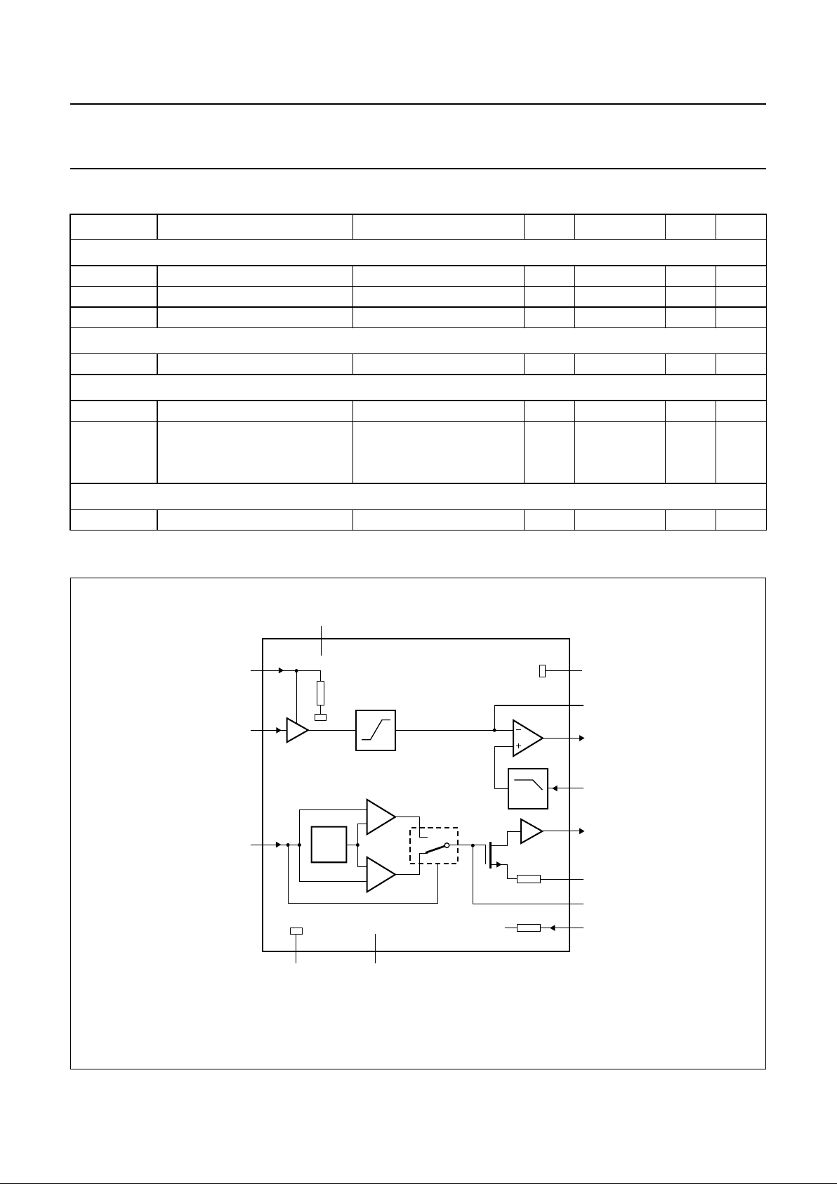
BLOCK DIAGRAM
SYMBOL PARAMETER CONDITIONS MIN. TYP. MAX. UNIT
Supplies
V
DD
supply voltage 2.4 − 5.5 V
I
DD
supply current − 3 − mA
V
DD(L)
laser supply voltage 2.4 − 5.5 V
RF amplifier
t
d(f)(RF)
RF flatness delay −− 10 ns
Laser supply circuit
I
o(LASER)(max)
maximum laser output current V
DD(L)
− V
o(LASER)
= 0.55 V 80 −−mA
V
i(mon)
monitor input voltage
N-substrate monitor diode − 0.150 − V
P-substrate monitor diode − V
DD
− 0.150 − V
Temperature range
T
amb
operating ambient temperature 0 − 70 °C
Fig.1 Block diagram.
(1) Band gap reference voltage.
handbook, full pagewidth
MBK902
250
kHz
8
TZA1025
14
3
7
10
1
12
9
V/I
V/I
V
DD(L)
V
DD
GND
26
V
GAP
MON
4
(1)
DIN
5
CDRW
11
V
DD
13
LD
CFIL
PWRON
RGADJ
CMFB
RFFB
RFEQO
GND
Page 4
1998 Oct 30 4
Philips Semiconductors Product specification
Data amplifier and laser supply circuit for CD
audio and video optical systems (ADALASLC)
TZA1025
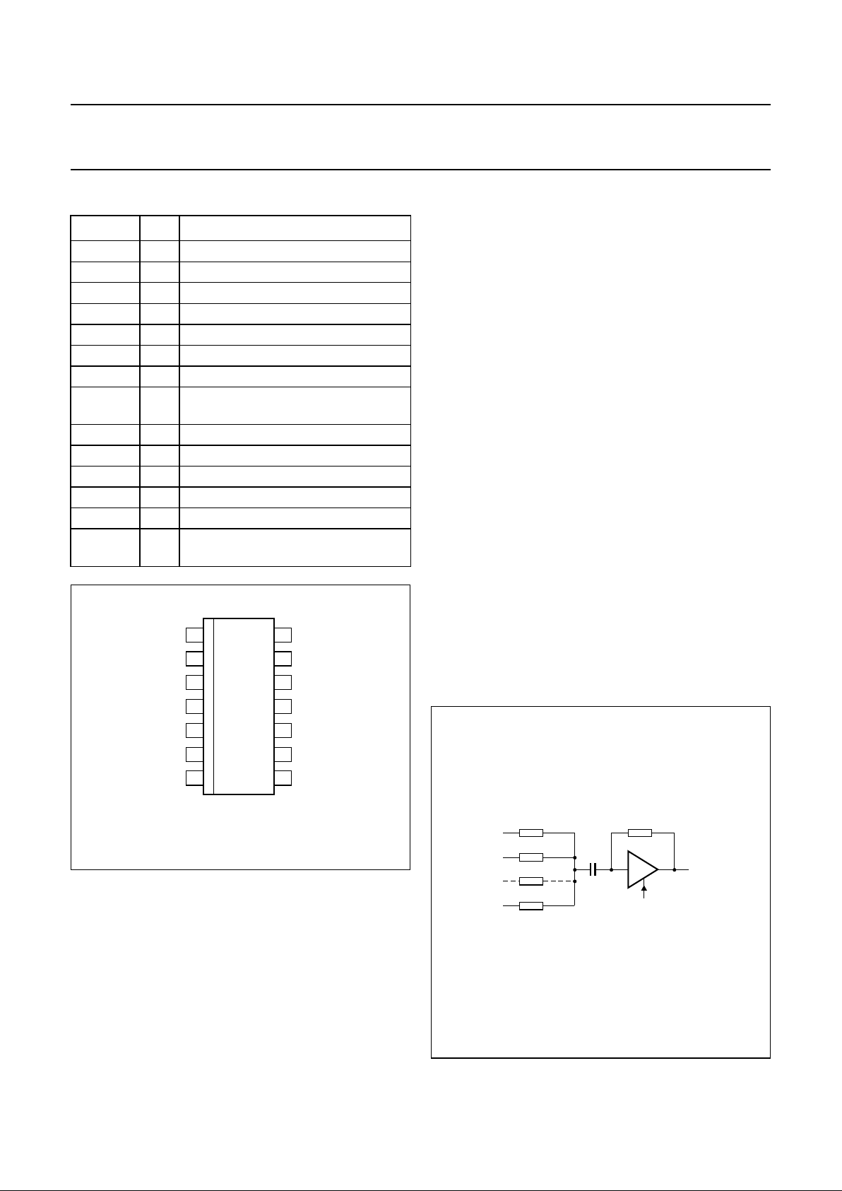
PINNING
FUNCTIONAL DESCRIPTION
The TZA1025 consists of two sections, the RF amplifier
and the automatic laser power control circuit.
RF amplifier
The RF amplifier consists of a current input amplifier, an
equalizer/bandwidth section and a transimpedance output
amplifier with an external feedback resistor of 10 kΩ(fixed
value).
SYMBOL PIN DESCRIPTION
LD 1 current output to laser diode
V
DD(L)
2 laser supply voltage
CFIL 3 external filter capacitor
MON 4 laser monitor diode input
DIN 5 central diode input
GND 6 ground
PWRON 7 power-on select input
CMFB 8 common mode feedback voltage
input
RFFB 9 external RF feedback resistor
RFEQO 10 RF amplifier output
CDRW 11 gain select input for CD-A/V, CD-R/W
GND 12 ground
V
DD
13 supply voltage
RGADJ 14 external laser supply gain adjust
resistor
Fig.2 Pin configuration.
handbook, halfpage
MBK901
TZA1025
1
2
3
4
5
6
7
8
14
13
12
11
10
9
LD
V
DD(L)
CFIL
MON
DIN
GND
PWRON
CMFB
RFFB
RFEQO
CDRW
GND
V
DD
RGADJ
The gain of the RF amplifier can be adjusted by the
external input resistors. Fig.3 shows the simplified
schematic which can be used to determine the RF gain.
The signal is AC coupled to the RF amplifier. The formula
to determine the gain is shown below:
(1)
where:
GRF is the RF amplifier gain
n is the number of input resistors
Z
tr(RF)
is the transimpedance of the amplifier (Ω)
R2 is the value of the input resistors (Ω).
The gain can be increased by a factor of 4 by making
pin CDRW HIGH. The value of Z
tr(RF)
is 9.8 kΩ for CD-A/V
(CDRW = LOW) and 38 kΩ for CD-R/W (CDRW = HIGH).
An internal equalizer ensures an optimal performance.
The DC output level of the amplifier can be set by applying
a DC voltage on the common mode feedback pin CMFB.
Since the input signal is AC-coupled the RF output voltage
will swing (symmetrically) around this DC level.
The coupling of the TZA1025 to the signal processor
(SAA7325) can be either AC or DC. When an AC-coupling
is chosen (see Fig.6) the minimum supply voltage can be
applied. When a DC-coupling is chosen (see Fig.7) a
minimum supply voltage of 2.8 V is required.
G
RF
n–
Z
tr RF()
R2
------------------
×=
Fig.3 Simplified schematic.
handbook, halfpage
CDRW
RFEQO
C2
10 kΩ
V
in
R2(1)
R2(2)
R2(n)
V
in
V
in
MGL530
Page 5
1998 Oct 30 5
Philips Semiconductors Product specification
Data amplifier and laser supply circuit for CD
audio and video optical systems (ADALASLC)
TZA1025
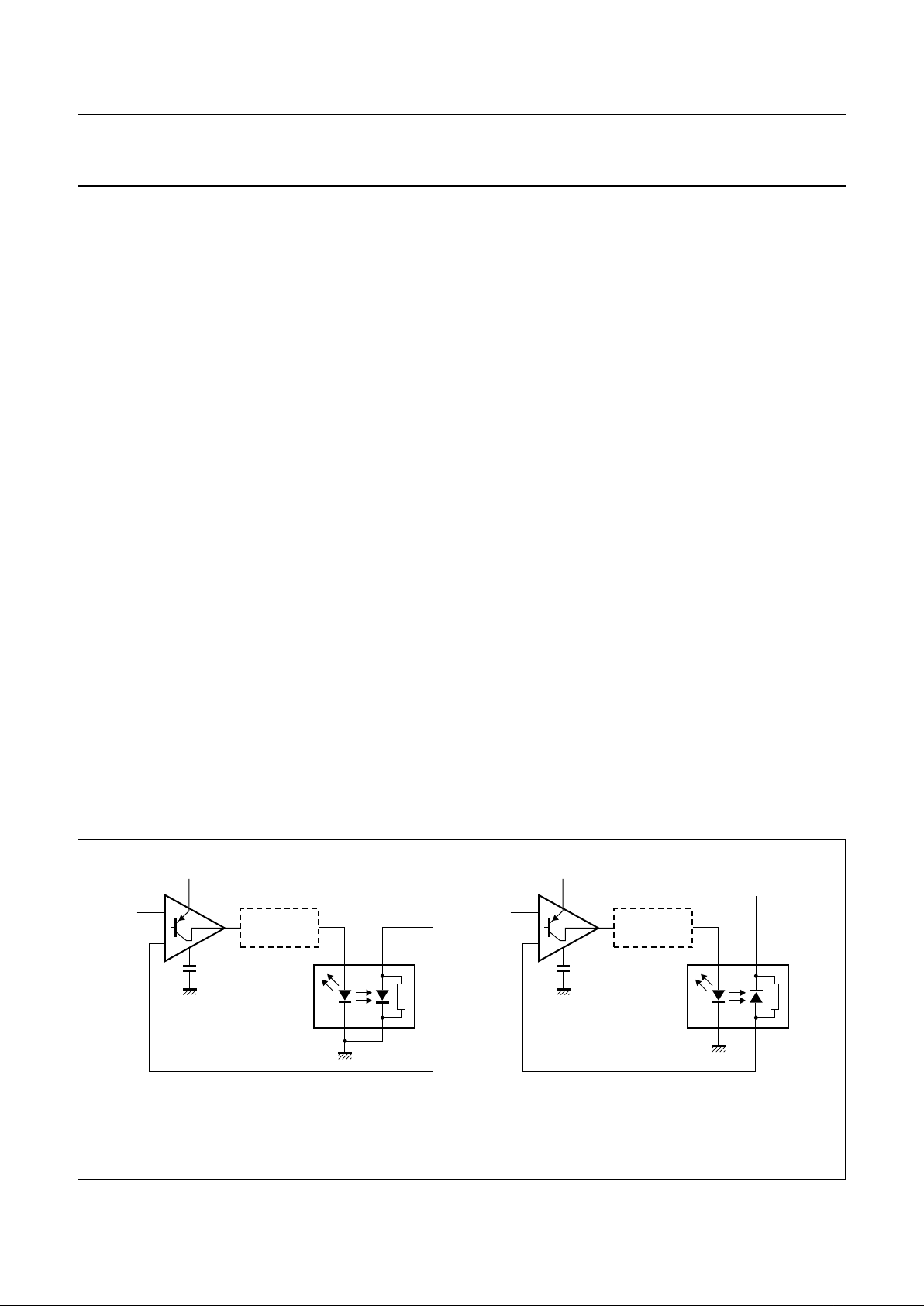
Automatic laser power control circuit
The ALPC stabilises the laser output power thereby
reducing the effect of ageing of the laser.
The TZA1025 automatically detects when an
N- or P-substrate monitor diode is used and selects the
correct reference voltage. A simplified diagram for the use
of an N- or P-substrate monitor diode is given in Fig.4.
The gain of the loop can be controlled (reduced) by adding
an external resistor between pins RGADJ and GND.
The loop gain then becomes:
(2)
where:
G
loop
is the loop gain
G
ALPC
is the ALPC transfer (60 A/V)
Glm is the laser-to-monitor transfer (V/A)
G
con
is the extra gain introduced when a DC-to-DC
converter is used in the loop; G
con
= 1 when no
DC-to-DC converter is used
250 is a fixed internal resistor value (Ω)
R
RGADJ
is the value of the external resistor (Ω).
The minimum available output current is also reduced
when an external resistor is used. The formula to
determine the minimum available output current is shown
in equation (3).
(3)
G
loop
G
ALPCGlm
× G
con
×
250
250 R
RGADJ
+
-------------------------------------
×=
I
oIo(LASER)(max)
250
250 R
RGADJ
+
-------------------------------------
×=
where:
I
o
is output current (mA)
I
o(LASER)(max)
is the maximum laser output current (mA)
250 is a fixed internal resistor value (Ω)
R
RGADJ
is the value of the external resistor (Ω).
The bandwidth of the loop is determined by the external
filter capacitor C
CFIL
and the loop gain. The formula to
determine the bandwidth is shown in equation (4).
(4)
where:
C
CFIL
is the value of the capacitor (F)
G
loop
is the loop gain.
The TZA1025 has a protection circuit to prevent laser
damage that can occur due to a dip of V
DD(L)
. When a dip
occurs the output transistor (see Fig.4) will go into
saturation making it unable to supply the required laser
current. Without the protection circuit the ALPC would still
try to supply the required laser current by charging the filter
capacitor C
CFIL
. After the dip a fully charged capacitor
would create a large output current during the few
milliseconds it needs to discharge the capacitor to a
normal level. The protection circuit monitors the output
transistor and switches off the ALPC when saturation
occurs by discharging the capacitor. The ALPC will
automatically restart within a few milliseconds after the dip
has passed.
τ
-3dB
C
CFIL
16 106⋅×
G
loop
----------------------------------------- -
=
Fig.4 Automatic Laser Power Control (ALPC) loop.
a. N-substrate monitor diode. b. P-substrate monitor diode.
handbook, full pagewidth
MGR519
DC-TO-DC
CONVERTER
C
CFIL
C
CFIL
V
DD(L)
150 mV
DC-TO-DC
CONVERTER
V
DD(L)
V
DD
VDD − 150 mV
Page 6

1998 Oct 30 6
Philips Semiconductors Product specification
Data amplifier and laser supply circuit for CD
audio and video optical systems (ADALASLC)
TZA1025
LIMITING VALUES
In accordance with the Absolute Maximum Rating System (IEC 134).
Notes
1. The maximum value V
DD
+ 0.5 must not exceed 5.5 V.
2. The maximum value V
DD(L)
+ 0.5 must not exceed 5.5 V.
3. Pins DIN and RFFB are current inputs with a limitation on the maximum input current.
4. The maximum peak current must not exceed ten times the absolute average input current with a maximum for the
absolute average input current of 1 mA. Averaging is only allowed over a maximum time interval of 100 ms.
5. Equivalent to discharging a 100 pF capacitor via a 1.5 kΩ series resistor with a rise time of 15 ns.
6. Equivalent to discharging a 200 pF capacitor via a 2.5 µH series inductor.
QUALITY SPECIFICATION
In accordance with
“SNW-FQ-611-E”
.
SYMBOL PARAMETER CONDITIONS MIN. MAX. UNIT
V
DD
supply voltage −0.5 +5.5 V
V
DD(L)
laser supply voltage −0.5 +5.5 V
V
i(n)
input voltage on pins 3, 4, 7, 8,
10, 11, 12 and 14
note 1 −0.5 VDD+ 0.5 V
V
o(LASER)
laser output voltage note 2 −0.5 V
DD(L)
+ 0.5 V
V
i(DIN)
central diode input voltage note 3 −0.5 − V
I
i(DIN)
central diode input current note 4 −1+1mA
V
i(RFFB)
RF feedback voltage note 3 −0.5 − V
I
i(RFFB)
RF feedback current note 4 −1+1mA
V
es
electrostatic handling human body model; note 5 −2000 +2000 V
machine model; note 6 −250 +250 V
T
amb
operating ambient temperature 0 70
°
C
Page 7

1998 Oct 30 7
Philips Semiconductors Product specification
Data amplifier and laser supply circuit for CD
audio and video optical systems (ADALASLC)
TZA1025
CHARACTERISTICS
VDD= 2.4 V; V
DD(L)
− V
o(LASER)
= 0.55 V; I
i(DIN)
= 0 mA; I
o(LASER)
= 80 mA; V
CMFB
=1⁄2VDD; PWRON = HIGH;
CDRW = LOW; C
CFIL
= 10 nF; R
RFFB
=10kΩ; pin RGADJ connected to ground; T
amb
=25°C; unless otherwise
specified.
SYMBOL PARAMETER CONDITIONS MIN. TYP. MAX. UNIT
Supplies
V
DD
supply voltage 2.4 − 5.5 V
V
DDL(L)
laser supply voltage 2.4 − 5.5 V
I
DD
supply current − 3 − mA
I
q
quiescent supply
current
PWRON = LOW −−40 µA
RF amplifier
I
i(DIN)
central diode input
current
−70 − +70 µA
Z
i(DIN)
central diode input
impedance
− 100 −Ω
V
CMFB
common mode
feedback input voltage
0.7
1
⁄2V
DD
VDD− 0.4 V
V
O(RFEQO)
RF amplifier output
DC-level
CDRW = LOW V
CMFB
− 0.05 − V
CMFB
+ 0.25 V
CDRW = HIGH V
CMFB
− 0.35 − V
CMFB
+ 0.35 V
V
o(RFEQO)
RF amplifier output
voltage
0.25 − VDD− 0.25 V
Z
o(RFEQO)
RF amplifier output
impedance
note 1 − 100 −Ω
t
d(f)(RF)
RF flatness delay −−10 ns
G
RF
RF path gain boost f = 720 kHz; note 2 − 5 − dB
Z
tr(RF)
RF transimpedance note 3
CDRW = LOW 9.2 9.8 10.4 kΩ
CDRW = HIGH 35.6 38 40.4 kΩ
THD
RF
RF total harmonic
distortion
note 4 −−50 − dB
PSRR
RF
RF power supply ripple
rejection
0 to 100 kHz − 40 − dB
V
n(in-band)(rm
s)
in-band noise
(RMS value)
note 4 − 2.7 − mV
Laser supply circuit
V
drop
drop voltage note 5 0.55 − 5.5 V
I
o(LASER)(max
)
maximum laser output
current
V
drop
= 0.55 V; note 6 80 −−mA
Z
o(LASER)
laser output impedance V
drop
= 0.55 V; note 7
I
o(LASER)
=53mA − 500 −Ω
I
o(LASER)
=20mA − 1200 −Ω
Page 8

1998 Oct 30 8
Philips Semiconductors Product specification
Data amplifier and laser supply circuit for CD
audio and video optical systems (ADALASLC)
TZA1025
Notes
1. Closed-loop output impedance (10 kΩ feedback resistor connected between pins RFEQO and RFFB).
2. G
RF
=(G
RFEQO
at fEQ) − (G
RFEQO
at 720 kHz).
3. Values to be used in equation (1).
4. An RF filter of 1 kΩ and 47 pF should be used on the RF output.
5. V
drop=VDD(L)
− V
o(LASER)
.
6. An external resistor can be used to reduce the maximum output current (and the gain) of the laser supply;
see equation (4).
7. The output impedance strongly depends on the drop voltage (V
drop
). The output impedance will approximately double
when the drop voltage doubles.
8.
9. When a voltage dip at V
DD(L)
occurs it could cause peak currents on I
o(LASER)
coming out of the ALPC output.
To protect the laser against such peak currents a protection circuit will switch-off the laser current when V
drop
becomes lower than V
clamp
. When V
drop>Vclamp
the laser will switch-on automatically again.
V
i(mon)
monitor input voltage
N-substrate 0.132 0.150 0.168 V
P-substrate V
DD
− 0.168 VDD− 0.150 VDD− 0.132 V
I
i(mon)
monitor input current −200 − +200 nA
t
sw(on)(LASER)
laser switch-on time − 3 − ms
RS
ref
reference supply
rejection
note 8 −−5%
V
clamp
ALPC clamp voltage note 9 −−0.5 V
Control inputs
Z
i(pd)
pull-down input
impedance pin CDRW
− 200 − kΩ
Z
i(pu)
pull-up input
impedance
pin PWRON
− 200 − kΩ
V
IL
LOW-level input
voltage
pin CDRW −0.2 −
1
⁄3V
DD
V
pin PWRON −0.2 −
1
⁄3V
DD
V
V
IH
HIGH-level input
voltage
pin CDRW
2
⁄3V
DD
− VDD+ 0.2 V
pin PWRON
2
⁄3V
DD
− VDD+ 0.2 V
SYMBOL PARAMETER CONDITIONS MIN. TYP. MAX. UNIT
RS
ref
∆V
mon
V
mon
----------------∆ V
DD
V
DD
-------------- -
----------------- -
=
Page 9

1998 Oct 30 9
Philips Semiconductors Product specification
Data amplifier and laser supply circuit for CD
audio and video optical systems (ADALASLC)
TZA1025
Fig.5 Equalizer gain and delay.
Definition of delay: t
d
ϕ
360
--------- -
f
---------------- -
=
(1) Gain.
(2) Delay.
handbook, halfpage
12
−4
MGR520
10
−1
110
0
4
8
246
248
250
252
254
G
(dB)
t
d
(ns)
f (MHz)
(2)
(1)
Page 10

1998 Oct 30 10
Philips Semiconductors Product specification
Data amplifier and laser supply circuit for CD
audio and video optical systems (ADALASLC)
TZA1025
APPLICATION INFORMATION
The application for the TZA1025 (ADALASLC) with the SAA7325 (CD10LC) using a coupling capacitor of 3.3 nF is
shown in Fig.6.
Fig.6 Application diagram with SAA7325 (CD10LC) using a coupling capacitor.
(1) See equation (3) to calculate the value of this resistor.
(2) Pin CDRW can be controlled by the CD10LC or a microprocessor but can also be fixed or switched by any other means.
(3) The 10 kΩ feedback resistor between pins 9 and 10 is a fixed value.
(4) The high-pass filter (AC-coupling) is placed at the input of the preamplifier. The −3 dB point (f = 10 kHz) is at
R2 Ω() C2 F()×
4
---------------------------------------------
MBK903
handbook, full pagewidth
10 nF
100 nF
100 nF
100 nF100 nF
TZA1025
(ADALASLC)
SAA7325
(CD10LC)
OPU
1
2
3
4
5
6
7
8
14
13
12
11
10
9
LD
V
DD(L)
CFIL
MON
DIN
GND
PWRON CMFB
RFFB
RFEQO
CDRW
GND
V
DD
RGADJ
R
RGADJ
(1)
LD
D1
D2
D3
D4
S1
S2
D1
D2
D3
D4
S1
S2
MON
VCOM
3.3 nF
HFIN
HFREF
ISLICE
LDON
VRIN
22
kΩ
10 kΩ
(3)
1 kΩ
47 pF
C2
(4)
V
DD(LASER)
V
DD
R2 (4×)
V
DD
LF FILTER
6 × 220 pF
from
microprocessor
(2)
Page 11

1998 Oct 30 11
Philips Semiconductors Product specification
Data amplifier and laser supply circuit for CD
audio and video optical systems (ADALASLC)
TZA1025
The application for the TZA1025 (ADALASLC) with the SAA7325 (CD10LC) without a coupling capacitor is shown in
Fig.7. A minimum supply voltage (VDD) is required for optimal performance.
Fig.7 Application diagram with SAA7325 (CD10LC) without coupling capacitor.
(1) See equation (3) to calculate the value of this resistor.
(2) Pin CDRW can be controlled by the CD10LC or a microprocessor but can also be fixed or switched by any other means.
(3) The 10 kΩ feedback resistor between pins 9 and 10 is a fixed value.
(4) The high-pass filter (AC-coupling) is placed at the input of the preamplifier. The −3 dB point (f = 10 kHz) is at
(5) The minimum supply voltage (VDD) without using a coupling capacitor is 2.8 V.
R2 Ω() C2 F()×
4
-------------------------------------------- -
MBK904
handbook, full pagewidth
10 nF
100 nF
100 nF
100 nF100 nF
TZA1025
(ADALASLC)
SAA7325
(CD10LC)
OPU
1
2
3
4
5
6
7
8
14
13
12
11
10
9
LD
V
DD(L)
CFIL
MON
DIN
GND
PWRON CMFB
RFFB
RFEQO
CDRW
GND
V
DD
RGADJ
R
RGADJ
(1)
LD
D1
D2
D3
D4
S1
S2
D1
D2
D3
D4
S1
S2
MON
VCOM
HFIN
HFREF
ISLICE
LDON
VRIN
10 kΩ
(3)
1 kΩ
47 pF
C2
(4)
V
DD(LASER)
V
DD
R2 (4×)
V
DD
(5)
from
microprocessor
(2)
LF FILTER
6 × 220 pF
Page 12

1998 Oct 30 12
Philips Semiconductors Product specification
Data amplifier and laser supply circuit for CD
audio and video optical systems (ADALASLC)
TZA1025
PACKAGE OUTLINE
UNIT
A
max.
A
1
A2A
3
b
p
cD
(1)E(1)
(1)
eHELLpQZywv θ
REFERENCES
OUTLINE
VERSION
EUROPEAN
PROJECTION
ISSUE DATE
IEC JEDEC EIAJ
mm
inches
1.75
0.25
0.10
1.45
1.25
0.25
0.49
0.36
0.25
0.19
8.75
8.55
4.0
3.8
1.27
6.2
5.8
0.7
0.6
0.7
0.3
8
0
o
o
0.25 0.1
DIMENSIONS (inch dimensions are derived from the original mm dimensions)
Note
1. Plastic or metal protrusions of 0.15 mm maximum per side are not included.
1.0
0.4
SOT108-1
X
w M
θ
A
A
1
A
2
b
p
D
H
E
L
p
Q
detail X
E
Z
e
c
L
v M
A
(A )
3
A
7
8
1
14
y
076E06S MS-012AB
pin 1 index
0.069
0.010
0.004
0.057
0.049
0.01
0.019
0.014
0.0100
0.0075
0.35
0.34
0.16
0.15
0.050
1.05
0.041
0.244
0.228
0.028
0.024
0.028
0.012
0.01
0.25
0.01 0.004
0.039
0.016
95-01-23
97-05-22
0 2.5 5 mm
scale
SO14: plastic small outline package; 14 leads; body width 3.9 mm
SOT108-1
Page 13

1998 Oct 30 13
Philips Semiconductors Product specification
Data amplifier and laser supply circuit for CD
audio and video optical systems (ADALASLC)
TZA1025
SOLDERING
Introduction
There is no soldering method that is ideal for all IC
packages. Wave soldering is often preferred when
through-hole and surface mounted components are mixed
on one printed-circuit board. However, wave soldering is
not always suitable for surface mounted ICs, or for
printed-circuits with high population densities. In these
situations reflow soldering is often used.
This text gives a very brief insight to a complex technology.
A more in-depth account of soldering ICs can be found in
our
“Data Handbook IC26; Integrated Circuit Packages”
(order code 9398 652 90011).
Reflow soldering
Reflow soldering techniques are suitable for all SO
packages.
Reflow soldering requires solder paste (a suspension of
fine solder particles, flux and binding agent) to be applied
to the printed-circuit board by screen printing, stencilling or
pressure-syringe dispensing before package placement.
Several techniques exist for reflowing; for example,
thermal conduction by heated belt. Dwell times vary
between 50 and 300 seconds depending on heating
method. Typical reflow temperatures range from
215 to 250 °C.
Preheating is necessary to dry the paste and evaporate
the binding agent. Preheating duration: 45 minutes at
45 °C.
Wave soldering
Wave soldering techniques can be used for all SO
packages if the following conditions are observed:
• A double-wave (a turbulent wave with high upward
pressure followed by a smooth laminar wave) soldering
technique should be used.
• The longitudinal axis of the package footprint must be
parallel to the solder flow.
• The package footprint must incorporate solder thieves at
the downstream end.
During placement and before soldering, the package must
be fixed with a droplet of adhesive. The adhesive can be
applied by screen printing, pin transfer or syringe
dispensing. The package can be soldered after the
adhesive is cured.
Maximum permissible solder temperature is 260 °C, and
maximum duration of package immersion in solder is
10 seconds, if cooled to less than 150 °C within
6 seconds. Typical dwell time is 4 seconds at 250 °C.
A mildly-activated flux will eliminate the need for removal
of corrosive residues in most applications.
Repairing soldered joints
Fix the component by first soldering two diagonallyopposite end leads. Use only a low voltage soldering iron
(less than 24 V) applied to the flat part of the lead. Contact
time must be limited to 10 seconds at up to 300 °C. When
using a dedicated tool, all other leads can be soldered in
one operation within 2 to 5 seconds between
270 and 320 °C.
Page 14

1998 Oct 30 14
Philips Semiconductors Product specification
Data amplifier and laser supply circuit for CD
audio and video optical systems (ADALASLC)
TZA1025
DEFINITIONS
LIFE SUPPORT APPLICATIONS
These products are not designed for use in life support appliances, devices, or systems where malfunction of these
products can reasonably be expected to result in personal injury. Philips customers using or selling these products for
use in such applications do so at their own risk and agree to fully indemnify Philips for any damages resulting from such
improper use or sale.
Data sheet status
Objective specification This data sheet contains target or goal specifications for product development.
Preliminary specification This data sheet contains preliminary data; supplementary data may be published later.
Product specification This data sheet contains final product specifications.
Limiting values
Limiting values given are in accordance with the Absolute Maximum Rating System (IEC 134). Stress above one or
more of the limiting values may cause permanent damage to the device. These are stress ratings only and operation
of the device at these or at any other conditions above those given in the Characteristics sections of the specification
is not implied. Exposure to limiting values for extended periods may affect device reliability.
Application information
Where application information is given, it is advisory and does not form part of the specification.
Page 15

1998 Oct 30 15
Philips Semiconductors Product specification
Data amplifier and laser supply circuit for CD
audio and video optical systems (ADALASLC)
TZA1025
NOTES
Page 16

Internet: http://www.semiconductors.philips.com
Philips Semiconductors – a worldwide company
© Philips Electronics N.V. 1998 SCA60
All rights are reserved. Reproduction in whole or in part is prohibited without the prior written consent of the copyright owner.
The information presented in this document does not form part of any quotation or contract, is believed to be accurate and reliable and may be changed
without notice. No liability will be accepted by the publisher for any consequence of its use. Publication thereof does not convey nor imply any license
under patent- or other industrial or intellectual property rights.
Middle East: see Italy
Netherlands: Postbus 90050, 5600 PB EINDHOVEN, Bldg. VB,
Tel. +31 40 27 82785, Fax. +31 40 27 88399
New Zealand: 2 Wagener Place, C.P.O. Box 1041, AUCKLAND,
Tel. +64 9 849 4160, Fax. +64 9 849 7811
Norway: Box 1, Manglerud 0612, OSLO,
Tel. +47 22 74 8000, Fax. +47 22 74 8341
Pakistan: see Singapore
Philippines: Philips Semiconductors Philippines Inc.,
106 Valero St. Salcedo Village, P.O. Box 2108 MCC, MAKATI,
Metro MANILA, Tel. +63 2 816 6380, Fax. +63 2 817 3474
Poland: Ul. Lukiska 10, PL 04-123 WARSZAWA,
Tel. +48 22 612 2831, Fax. +48 22 612 2327
Portugal: see Spain
Romania: see Italy
Russia: Philips Russia, Ul. Usatcheva 35A, 119048 MOSCOW,
Tel. +7 095 755 6918, Fax. +7 095 755 6919
Singapore: Lorong 1, Toa Payoh, SINGAPORE 319762,
Tel. +65 350 2538, Fax. +65 251 6500
Slovakia: see Austria
Slovenia: see Italy
South Africa: S.A. PHILIPS Pty Ltd., 195-215 Main Road Martindale,
2092 JOHANNESBURG, P.O. Box 7430 Johannesburg 2000,
Tel. +27 11 470 5911, Fax. +27 11 470 5494
South America: Al. Vicente Pinzon, 173, 6th floor,
04547-130 SÃO PAULO, SP, Brazil,
Tel. +55 11 821 2333, Fax. +55 11 821 2382
Spain: Balmes 22, 08007 BARCELONA,
Tel. +34 93 301 6312, Fax. +34 93 301 4107
Sweden: Kottbygatan 7, Akalla, S-16485 STOCKHOLM,
Tel. +46 8 5985 2000, Fax. +46 8 5985 2745
Switzerland: Allmendstrasse 140, CH-8027 ZÜRICH,
Tel. +41 1 488 2741 Fax. +41 1 488 3263
Taiwan: Philips Semiconductors, 6F, No. 96, Chien Kuo N. Rd., Sec. 1,
TAIPEI, Taiwan Tel. +886 2 2134 2865, Fax. +886 2 2134 2874
Thailand: PHILIPS ELECTRONICS (THAILAND) Ltd.,
209/2 Sanpavuth-Bangna Road Prakanong, BANGKOK 10260,
Tel. +66 2 745 4090, Fax. +66 2 398 0793
Turkey: Talatpasa Cad. No. 5, 80640 GÜLTEPE/ISTANBUL,
Tel. +90 212 279 2770, Fax. +90 212 282 6707
Ukraine: PHILIPS UKRAINE, 4 Patrice Lumumba str., Building B, Floor 7,
252042 KIEV, Tel. +380 44 264 2776, Fax. +380 44 268 0461
United Kingdom: Philips Semiconductors Ltd., 276 Bath Road, Hayes,
MIDDLESEX UB3 5BX, Tel. +44 181 730 5000, Fax. +44 181 754 8421
United States: 811 East Arques Avenue, SUNNYVALE, CA 94088-3409,
Tel. +1 800 234 7381
Uruguay: see South America
Vietnam: see Singapore
Yugoslavia: PHILIPS, Trg N. Pasica 5/v, 11000 BEOGRAD,
Tel. +381 11 625 344, Fax.+381 11 635 777
For all other countries apply to: Philips Semiconductors,
International Marketing & Sales Communications, Building BE-p, P.O. Box 218,
5600 MD EINDHOVEN, The Netherlands, Fax. +31 40 27 24825
Argentina: see South America
Australia: 34 Waterloo Road, NORTH RYDE, NSW 2113,
Tel. +61 2 9805 4455, Fax. +61 2 9805 4466
Austria: Computerstr. 6, A-1101 WIEN, P.O. Box 213, Tel. +43 160 1010,
Fax. +43 160 101 1210
Belarus: Hotel Minsk Business Center, Bld. 3, r. 1211, Volodarski Str. 6,
220050 MINSK, Tel. +375 172 200 733, Fax. +375 172 200 773
Belgium: see The Netherlands
Brazil: seeSouth America
Bulgaria: Philips Bulgaria Ltd., Energoproject, 15thfloor,
51 James Bourchier Blvd., 1407 SOFIA,
Tel. +359 2 689 211, Fax. +359 2 689 102
Canada: PHILIPS SEMICONDUCTORS/COMPONENTS,
Tel. +1 800 234 7381
China/Hong Kong: 501 Hong Kong Industrial Technology Centre,
72 Tat Chee Avenue, Kowloon Tong, HONG KONG,
Tel. +852 2319 7888, Fax. +852 2319 7700
Colombia: see South America
Czech Republic: see Austria
Denmark: Prags Boulevard 80, PB 1919, DK-2300 COPENHAGEN S,
Tel. +45 32 88 2636, Fax. +45 31 57 0044
Finland: Sinikalliontie 3, FIN-02630 ESPOO,
Tel. +358 9 615800, Fax. +358 9 61580920
France: 51 Rue Carnot, BP317, 92156 SURESNES Cedex,
Tel. +33 1 40 99 6161, Fax. +33 1 40 99 6427
Germany: Hammerbrookstraße 69, D-20097 HAMBURG,
Tel. +49 40 23 53 60, Fax. +49 40 23 536 300
Greece: No. 15, 25th March Street, GR 17778 TAVROS/ATHENS,
Tel. +30 1 4894 339/239, Fax. +30 1 4814 240
Hungary: seeAustria
India: Philips INDIA Ltd, Band Box Building, 2nd floor,
254-D, Dr. Annie Besant Road, Worli, MUMBAI 400 025,
Tel. +91 22 493 8541, Fax. +91 22 493 0966
Indonesia: PT Philips Development Corporation, Semiconductors Division,
Gedung Philips, Jl. Buncit Raya Kav.99-100, JAKARTA 12510,
Tel. +62 21 794 0040 ext. 2501, Fax. +62 21 794 0080
Ireland: Newstead, Clonskeagh, DUBLIN 14,
Tel. +353 1 7640 000, Fax. +353 1 7640 200
Israel: RAPAC Electronics, 7 Kehilat Saloniki St, PO Box 18053,
TEL AVIV 61180, Tel. +972 3 645 0444, Fax. +972 3 649 1007
Italy: PHILIPS SEMICONDUCTORS, Piazza IV Novembre 3,
20124 MILANO, Tel. +39 2 6752 2531, Fax. +39 2 6752 2557
Japan: Philips Bldg 13-37, Kohnan 2-chome, Minato-ku,
TOKYO 108-8507, Tel. +81 3 3740 5130, Fax. +81 3 3740 5077
Korea: Philips House, 260-199 Itaewon-dong, Yongsan-ku, SEOUL,
Tel. +82 2 709 1412, Fax. +82 2 709 1415
Malaysia: No. 76 Jalan Universiti, 46200 PETALING JAYA, SELANGOR,
Tel. +60 3 750 5214, Fax. +60 3 757 4880
Mexico: 5900 Gateway East, Suite 200, EL PASO, TEXAS 79905,
Tel. +9-5 800 234 7381
Printed in The Netherlands 545102/00/01/pp16 Date of release: 1998 Oct 30 Document order number: 9397 750 04251
 Loading...