

Page 1

DATA SH EET
Product specification
Supersedes data of 1998 Sep 09
File under Integrated Circuits, IC01
1999 Aug 19
INTEGRATED CIRCUITS
TZA1015
Data amplifier and laser supply
circuit for CD and read-only optical
systems (HDALAS)
Page 2

1999 Aug 19 2
Philips Semiconductors Product specification
Data amplifier and laser supply circuit for CD
and read-only optical systems (HDALAS)
TZA1015
FEATURES
• Six input buffer amplifiers with low-pass filtering and
virtually no offset
• Universal photodiode IC interface using internal
conversion resistors
• RFdataamplifierwith widebandwidth designed fordata
rates up to a maximum of 30×
• Programmable RFgain forCD-A/V, CD-R,CD-R/W and
CD-ROM applications
• Programmable RF bandwidth for optimal playability
• Radial error signal for fast track counting
• Programmable RF/Fast Track Count (FTC) gain for
optimal dynamic range
• Fully automatic laser control including stabilization and
on/off switch plusa separate supply for powerefficiency
• Automatic monitor diode polarity selection
• Adjustable laser bandwidth and laser switch-on current
slope using external capacitor
• Protection circuitto prevent laserdamage dueto supply
voltage dip
• Optimized interconnection between data amplifier and
Philips’ digital signal processor family (CD7, ACE and
MACE)
• Wide supply voltage range
• Wide temperature range
• Low power consumption.
GENERAL DESCRIPTION
TheTZA1015 isa dataamplifierand lasersupply circuitfor
3-beam pick-updetectors foundin awide rangeof CD and
read-only optical systems.
The device contains 6 transimpedance amplifiers to
amplify and filter the focus and radial photo diode voltage
input signals. The preamplifier forms a versatile,
programmable interface from voltage output CD
mechanisms to the Philips’ digital signal processor family.
The dynamic range of this preamplifier/processor
combination can be optimized for the LF servo and RF
data paths. The servo channel gain is set by the ADC
range of the processor. The RF data channel can be
programmed in the TZA1015 preamplifier.
The programmable RF bandwidthallows this device to be
used in CD-A/V applications or CD-R, CD-R/W and
CD-ROM applicationswith adata rate upto amaximum of
30×. The RF and LF gain can be adapted for CD-A/V,
CD-R andCD-ROM discs or CD-R/Wdiscs by meansof a
gain switch. In addition to this gain switch the RF gain is
programmable toguarantee optimal playability.In orderto
enable minimal access time the TZA1015 generates a
Fast Track Count signal which enables the decoder
(ACE or MACE) to count the number of tracks during a
track jump.
The device canaccommodate astigmatic, single Foucault
and double Foucault detectors and can be used with all
laserand N-orP-sub monitordiodes.The AutomaticLaser
Power Control(ALPC) circuit willmaintain controlover the
laser diode current. With an on-chip reference voltage
generator, a constant and stabilized output power is
ensured independent of ageing. Aseparate power supply
connection allows the internal power dissipation to be
reduced by connecting a low voltage supply.
ORDERING INFORMATION
TYPE NUMBER
PACKAGE
NAME DESCRIPTION VERSION
TZA1015T SO28 plastic small outline package; 28 leads; body width 7.5 mm SOT136-1
Page 3

1999 Aug 19 3
Philips Semiconductors Product specification
Data amplifier and laser supply circuit for CD
and read-only optical systems (HDALAS)
TZA1015
QUICK REFERENCE DATA
SYMBOL PARAMETER CONDITIONS MIN. TYP. MAX. UNIT
Supply
V
DD(RF,LF)
supply voltage 4.5 5.0 5.5 V
V
DD(L)
laser supply voltage 3 − 5.5 V
LF amplifiers
I
OS
channel matching −− 1 %FS
B
(−3dB)
−3 dB bandwidth 65 90 115 kHz
RF amplifier
B
(−3dB)
−3 dB bandwidth programmable;
GARF = open-circuit
− 10 − MHz
− 20 − MHz
− 50 − MHz
t
d(f)(RF)
RF flatness delay −− 0.4 ns
Laser supply
I
o(LASER)(min)
minimum laser output current V
DD(L)
=3V −− 100 mA
V
i(mon)
monitor input voltage
N-type monitor − 0.150 − V
P-type monitor − V
DD(RF,LF)
− 0.150 − V
Temperature range
T
oper
operating temperature 0 − 85 °C
T
stg
storage temperature −65 − +150 °C
Page 4
1999 Aug 19 4
Philips Semiconductors Product specification
Data amplifier and laser supply circuit for CD
and read-only optical systems (HDALAS)
TZA1015
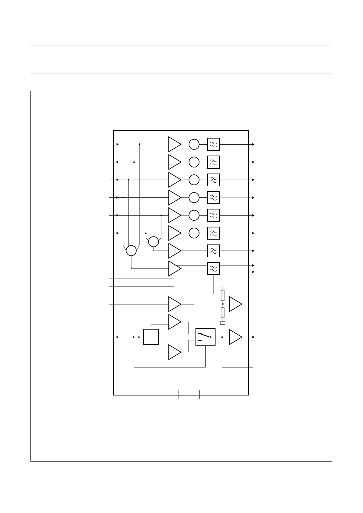
BLOCK DIAGRAM
Fig.1 Block diagram.
(1) Bandgap reference voltage.
handbook, full pagewidth
MGK356
V/I
V/I
V/I
+
+
+
−
+
+
+
+
−
+
−
+
−
+
−
+
−
+
−
+
LD
V
DD(L)
CFIL
V
DD(LF)
V
DD(LF)
V
ref
RFN
RFP
V
DD(RF)
O1
O2
O3
O4
O5
O6
GND PWRON
FTC
2
3
4
12
26
25
2423
22
21
20
19
18
17
16
15
14
TZA1015
V
GAP
RFBWS
MON
D1
D2
D3
D4
S5
S6
V
COM
GARF
GSE
1
5
6
7
8
9
10
11
13
28
27
(1)
Page 5
1999 Aug 19 5
Philips Semiconductors Product specification
Data amplifier and laser supply circuit for CD
and read-only optical systems (HDALAS)
TZA1015
PINNING
SYMBOL PIN DESCRIPTION
RFBWS 1 RF amplifier bandwidth select
LD 2 current output to the laser diode
V
DD(L)
3 laser supply voltage
CFIL 4 external filter capacitor
MON 5 laser monitor diode input
D1 6 input photo diode amplifier 1 (central)
D2 7 input photo diode amplifier 2 (central)
D3 8 input photo diode amplifier 3 (central)
D4 9 input photo diode amplifier 4 (central)
S5 10 input photo diode amplifier 5
(satellite)
S6 11 input photo diode amplifier 6
(satellite)
V
DD(LF)
12 LF diode and FTC amplifier supply
voltage
V
COM
13 common mode DC reference input
V
ref
14 DC reference voltage for biasing of
Opto Electronic IC (OEIC)
FTC 15 fast track count amplifier output
PWRON 16 power on/off switch (V
ref
bias
generator always active)
O6 17 output photo diode amplifier 6
O5 18 output photo diode amplifier 5
O4 19 output photo diode amplifier 4
O3 20 output photo diode amplifier 3
O2 21 output photo diode amplifier 2
O1 22 output photo diode amplifier 1
V
DD(RF)
23 RF amplifier supply voltage
GND 24 ground
RFP 25 positive output RF data amplifier
RFN 26 negative output RF data amplifier
GSE 27 gain select for CD, CD-R, CD-R/W;
RF and FTC amplifiers
GARF 28 gain adjust for RF and FTC amplifiers
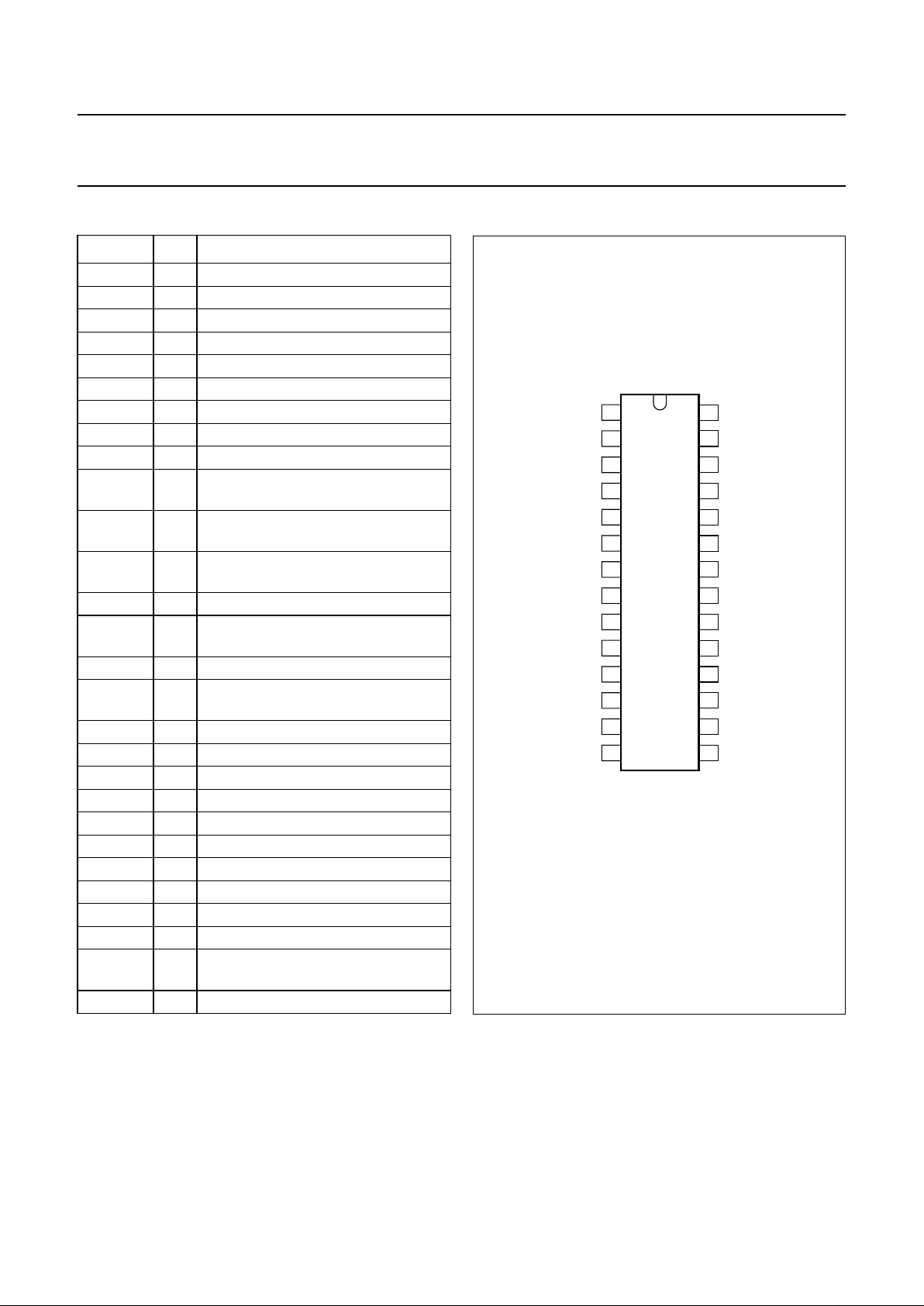
Fig.2 Pin configuration.
handbook, halfpage
RFBWS
LD
V
DD(L)
CFIL
MON
D1
D2
D3
D4
S5
S6
V
DD(LF)
V
COM
V
ref
GARF
GSE
RFN
RFP
V
DD(RF)
O1
O2
O3
O4
O5
O6
GND
PWRON
FTC
1
2
3
4
5
6
7
8
9
10
11
12
13
28
27
26
25
24
23
22
21
20
19
18
17
16
1514
TZA1015
MGK355
Page 6

1999 Aug 19 6
Philips Semiconductors Product specification
Data amplifier and laser supply circuit for CD
and read-only optical systems (HDALAS)
TZA1015
LIMITING VALUES
In accordance with the Absolute Maximum Rating System (IEC 134).
Note
1. Based on standard measurement for determining thermal resistance of the package. In accordance with
MIL-STD 883C.
CHARACTERISTICS
V
DD(LF)=VDD(RF)=VDD(L)
= 5.0 V; T
amb
=25°C; PWRON = HIGH; GSE = LOW; GARF = open-circuit;
RFBWS = HIGH; DC input voltagesat pins V
COM
, D1 to D4, S5 and S6 =1⁄2VDD; output voltageat pins O1 to O6 = 0 V;
I
DD(L)(d)
= 50 mA; C
CFIL
= 1 nF; unless otherwise specified. Diode input voltages all with respect to V
COM
.
SYMBOL PARAMETER CONDITIONS MIN. MAX. UNIT
V
DD(RF,LF)
supply voltage −0.5 +5.5 V
V
I(n)
input voltage for all pins −0.5 V
DD(RF,LF)
+ 0.5 V
I
source
source current
pin FTC − 4mA
pin RFP − 2mA
pin RFN − 2mA
T
amb
operating ambient temperature −40 +100 °C
P
max
maximum power dissipation note 1 − 700 mW
SYMBOL PARAMETER CONDITIONS MIN. TYP. MAX. UNIT
Supplies
V
DD(RF,LF)
supply voltage 4.5 5.0 5.5 V
V
DD(L)
laser supply
voltage
3 − 5.5 V
I
DD(LF)
LF supply current − 13 − mA
I
DD(RF)
RF supply current − 20 − mA
I
DD(L)(d)
laser diode supply
current
− 50 100 mA
I
q
quiescent supply
current
PWRON = LOW −− 6mA
Input voltages
V
i(D1-D4,S5,S6)
inputsignal voltage
range(with respect
to V
COM
)
all inputs;
GSE = LOW
0 − 0.6 V
all inputs;
GSE = HIGH
0 − 0.15 V
V
I(CM)
common mode DC
reference input
voltage range
1.6 − V
DD(RF,LF)
− 2.2 V
Page 7

1999 Aug 19 7
Philips Semiconductors Product specification
Data amplifier and laser supply circuit for CD
and read-only optical systems (HDALAS)
TZA1015
LF diode amplifiers
Z
CONV
conversion
impedance
central diodes,
D1 to D4
GSE = LOW 40 47 54 kΩ
GSE = HIGH 10.5 12.5 15.0 kΩ
satellite diodes,
S5 and S6
GSE = LOW 75 92 106 kΩ
GSE = HIGH 20.5 24.5 28 kΩ
I
o(LF)
output current
range
note 1
central diodes,
O1 to O4
0 − 12 µA
satellite diodes,
O5 and O6
0 − 6 µA
V
O(LF)
DC output voltage
range central and
satellite diodes
−0.2 − V
DD(RF,LF)
− 2.1 V
Z
i
input impedance
central diodes − 3.1 − pF
satellite diodes − 3.1 − pF
I
OS
channel pair
matching
note 2
central diodes,
O1 to O4
−1 − +1 %FS
satellite diodes,
O5 and O6
−2 − +2 %FS
B
(−3dB)
−3 dB bandwidth
central diodes,
D1 to D4
65 90 115 kHz
satellite diodes,
S5 and S6
65 90 115 kHz
RF amplifier
V
O(RFP)
DC output level
RFP
GSE = LOW or
HIGH;
V
i(D1 to D4)
=0V
0.25 0.5 0.7 V
V
O(RFN)
DC output level
RFN
GSE = LOW or
HIGH;
V
i(D1 to D4)
=0V
2.6 3.1 3.4 V
V
o(RF)(dif)
differential RF
output signal
(V
o(RFP)
− V
o(RFN)
)
note 3 − 2 − V
V
o(RF)
single-sided RF
output signal
note 3 − 1 − V
Z
o(RF)
RF output
impedance
− 25 −Ω
SYMBOL PARAMETER CONDITIONS MIN. TYP. MAX. UNIT
Page 8

1999 Aug 19 8
Philips Semiconductors Product specification
Data amplifier and laser supply circuit for CD
and read-only optical systems (HDALAS)
TZA1015
G
RF
RF path gain note 4
GSE = LOW 9 10.5 12 dB
GSE = HIGH 21 22.5 24 dB
t
d(f)(RF)
RF flatness delay GSE = LOW or
HIGH; note 5
f < 5 MHz;
RFBWS = LOW
−− 2.0 ns
f < 10 MHz;
RFBWS =
open-circuit
−− 1.0 ns
f < 25 MHz;
RFBWS = HIGH
−− 0.4 ns
B
RF(−3dB)
−3 dB bandwidth
(RF signal)
GSE = LOW or
HIGH
RFBWS = LOW − 10 − MHz
RFBWS =
open-circuit
− 20 − MHz
RFBWS = HIGH − 50 − MHz
V
n(in-band)(rms)
in-band noise
(RMS value)
RFBWS = LOW − 1.0 − mV
RFBWS =
open-circuit
− 1.4 − mV
RFBWS = HIGH − 2.1 − mV
V
O(FTC)
fasttrack count DC
output level
GSE = LOW or
HIGH; note 6
1.3 1.5 1.7 V
G
FTC
fast track count
gain
f = 100 kHz;
note 7
GSE = LOW 16.5 18 19.5 dB
GSE = HIGH 26.5 28 29.5 dB
B
FTC(−3dB)
fast track count
−3 dB bandwidth
220 300 380 kHz
Laser supply (APC)
I
o(LASER)(min)
minimum laser
output current
−− 100 mA
V
i(mon)
monitor input
voltage
N-type −10% 0.150 +13.5% V
P-type − V
DD(RF,LF)
− 0.150 − V
V
o(LASER)
laser output
voltage range
I
o(LASER)
= 100 mA −− V
DD(L)
− 1.2 V
t
sw(on)(LASER)
laser switch-on
time
− 3 − ms
I
i(mon)
monitor input
current
−− 100 nA
SYMBOL PARAMETER CONDITIONS MIN. TYP. MAX. UNIT
Page 9

1999 Aug 19 9
Philips Semiconductors Product specification
Data amplifier and laser supply circuit for CD
and read-only optical systems (HDALAS)
TZA1015
Control inputs
Z
i(pd)
pull-down input
impedance
(pin GSE)
− 150 − kΩ
Z
i(pu)
pull-up input
impedance
(pin PWRON)
− 150 − kΩ
V
IL
LOW-level input
voltage
pins GSE
and PWRON
−0.2 − V
pins GARF
and RFBWS
−0.2 − +0.5 V
V
IH
HIGH-level input
voltage
pins GSE
and PWRON
− V
DD(RF,LF)
+ 0.2 V
pins GARF
and RFBWS
V
DD(RF,LF)
− 0.5 − V
DD(RF,LF)
+ 0.2 V
I
IL
LOW-level input
current
(pins GARF
and RFBWS)
−− −70 µA
I
IH
HIGH-level input
current
(pins GARF
and RFBWS)
−− 80 µA
V
ref
voltage source
V
O
DC output voltage −10% +10% V
I
O
output current
range
sink 1.5 −−mA
source −− −3mA
Z
O
DC output
impedance
−− 30 Ω
SYMBOL PARAMETER CONDITIONS MIN. TYP. MAX. UNIT
V
DD(RF,LF)
3.3
--------------------------
V
DD(RF,LF)
1.4
--------------------------
V
DD(RF,LF)
2
------------------------- -
Page 10

1999 Aug 19 10
Philips Semiconductors Product specification
Data amplifier and laser supply circuit for CD
and read-only optical systems (HDALAS)
TZA1015
Notes
1. The output current can be increased but does not match the default input range of the servo system.
2. Matching defined in % of FS output per channel pairs (O1 − O2), (O3 − O4), (S5 − S6), at1⁄3and2⁄3 of full output
scale.
3. V
o(RFP)=Vo(RF)
; V
o(RFN)
= −V
o(RF)
.
4. Gain is defined as:
All inputs assumed to be equal: , where i=1to4 and D means diode.
5. See Figs 3, 4 and 5.
6. Voltage is based on 2 PN junctions and is temperature dependent.
7. Gain is defined as:
G
RF
20
V
oRFP()
V
iLF()
--------------------
log× 20
V
oRFN()
V
iLF()
--------------------
log×==
V
i(LF)
ΣV
i(D)
4
---------------
=
G
FTC
20
V
oFTC()
V
iS5()ViS6()
–()
---------------------------------------- -
log×=
Fig.3 Gain and delay for 50 MHz bandwidth.
Definition of delay: delay
ϕ
360
--------- -
f
---------------
=
(1) Gain.
(2) Delay.
handbook, halfpage
12
7
10
−1
1
10
f (MHz)
10
2
MGK357
8
9
10
11
9.00
7.75
8.00
8.25
8.50
8.75
G
(dB)
t
d
(ns)
(1)
(2)
Fig.4 Gain and delay for 20 MHz bandwidth.
Definition of delay: delay
ϕ
360
--------- -
f
---------------
=
(1) Gain.
(2) Delay.
handbook, halfpage
12
7
10
−1
1
10
f (MHz)
10
2
MGK358
8
9
10
11
14.5
12.0
12.5
13.0
13.5
14.0
G
(dB)
t
d
(ns)
(1)
(2)
Page 11

1999 Aug 19 11
Philips Semiconductors Product specification
Data amplifier and laser supply circuit for CD
and read-only optical systems (HDALAS)
TZA1015
Table 1 Control inputs, conversion impedances and gain settings
Table 2 Control inputs and RF bandwidth
PIN GSE PIN GARF
NOMINAL LF V/I
CONVERSION
(CENTRAL DIODES)
NOMINAL LF V/I
CONVERSION
(SATELLITE DIODES)
NOMINAL RF
GAIN (dB)
NOMINAL FTC
GAIN (dB)
LOW LOW 47 kΩ 92 kΩ 7 14
LOW open-circuit 47 kΩ 92 kΩ 10.5 18
LOW HIGH 47 kΩ 92 kΩ 15 22
HIGH LOW 12.5 kΩ 24.5 kΩ 19 24
HIGH open-circuit 12.5 kΩ 24.5 kΩ 22.5 28
HIGH HIGH 12.5 kΩ 24.5 kΩ 27 32
PIN RFBWS RF AMPLIFIER BANDWIDTH
LOW 10 MHz
open-circuit 20 MHz
HIGH 50 MHz
Fig.5 Gain and delay for 10 MHz bandwidth.
Definition of delay: delay
ϕ
360
--------- -
f
---------------
=
(1) Gain.
(2) Delay.
handbook, halfpage
12
7
10
−1
1
10
f (MHz)
10
2
MGK359
8
9
10
11
23
13
15
17
19
21
G
(dB)
t
d
(ns)
(1)
(2)
Page 12

1999 Aug 19 12
Philips Semiconductors Product specification
Data amplifier and laser supply circuit for CD
and read-only optical systems (HDALAS)
TZA1015
APPLICATION INFORMATION
The circuits shown in Figs 6 and 7 are applications for the TZA1015 (HDALAS) with the SAA7370A (CD7) or the
SAA7348 (ACE).
handbook, full pagewidth
22
kΩ
RFBWS
LD
V
DD(L)
CFIL
MON
D1
D2
D3
D4
S5
S6
V
DD(LF)
V
DD(RF, LF)
V
COM
V
ref
LD
MON
D1
D2
D3
D4
S5
S6
V
ref
GARF
GSE
RFN
RFP
V
DD(RF)
O1
O2
O3
O4
O5
O6
GND
PWRON
FTC
1
2
3
4
5
6
7
8
9
10
11
12
13
28
27
26
25
24
23
22
21
20
19
18
17
16
1514
TZA1015
(HDALAS)
MGK360
ISLICE
I
ref
HFIN
HFREF
D1
D2
D3
D4
R1
R2
LDON
6 × 220 pF
V
RL
14
18
15
17
3
4
5
7
8
9
64
6
SAA7370A
(CD7)
100 nF
100 nF
1 nF
1 nF
100
nF
R1
(2)
C1
(2)
100
nF
V
DD(RF, LF)
V
DD(LASER)
100 nF
1 nF
OPIC
R2
(2)
22
kΩ
100
nF
from
microprocessor
(1)
from
microprocessor
(1)
to
microprocessor
(3)
Fig.6 Application diagram with SAA7370A (CD7).
(1) Pins RFBWS, GARF and GSE can be microprocessor controlled but can also be fixed or switched by any other means.
(2) For recommended values per speed see Table 3.
(3) The FTC output is available for optional processing.
Page 13

1999 Aug 19 13
Philips Semiconductors Product specification
Data amplifier and laser supply circuit for CD
and read-only optical systems (HDALAS)
TZA1015
Fig.7 Application diagram with SAA7348 (ACE).
(1) Pins RFBWS, GARF and GSE can be microprocessor controlled but can also be fixed or switched by any other means.
(2) For recommended values per speed see Table 4.
handbook, full pagewidth
47
kΩ
5
pF
22 nF
RFBWS
LD
V
DD(L)
CFIL
MON
D1
D2
D3
D4
S5
S6
V
DD(LF)
V
DD(RF, LF)
V
COM
V
ref
LD
MON
D1
D2
D3
D4
S5
S6
V
ref
GARF
GSE
RFN
RFP
V
DD(RF)
O1
O2
O3
O4
O5
O6
GND
PWRON
FTC
1
2
3
4
5
6
7
8
9
10
11
12
13
28
27
26
25
24
23
22
21
20
19
18
17
16
1514
TZA1015
(HDALAS)
MGK361
HFIN
D1
D2
D3
D4
S1
S2
LDON
FTC
H
from
microprocessor
(1)
from
microprocessor
(1)
9
15
16
17
20
21
22
100
24
FTC
L
25
SAA7348
(ACE)
100 nF
100 nF
1 nF
68 nF
R1
(2)
C1
(2)
100
nF
V
DD(RF, LF)
V
DD(LASER)
100 nF
OPIC
Table 3 Recommended values of components per
speed for application diagram of Fig.6
Table 4 Recommended values of components per
speed for application diagram of Fig.7
N C1R1R2
1×47 pF 1 kΩ 1kΩ
2× 47 pF 470 Ω 470 Ω
4× 22 pF 470 Ω 470 Ω
8× 10 pF 470 Ω 470 Ω
10× 8.2 pF 470 Ω 470 Ω
NC1R1
1×100 pF 1 kΩ
2× 47 pF 1 kΩ
4× 22 pF 1 kΩ
8× 22 pF 470 Ω
16× 10 pF 470 Ω
18× 6.8 pF 470 Ω
Page 14

1999 Aug 19 14
Philips Semiconductors Product specification
Data amplifier and laser supply circuit for CD
and read-only optical systems (HDALAS)
TZA1015
PACKAGE OUTLINE
UNIT
A
max.
A
1
A2A
3
b
p
cD
(1)E(1) (1)
eHELLpQ
Z
ywv θ
REFERENCES
OUTLINE
VERSION
EUROPEAN
PROJECTION
ISSUE DATE
IEC JEDEC EIAJ
mm
inches
2.65
0.30
0.10
2.45
2.25
0.49
0.36
0.32
0.23
18.1
17.7
7.6
7.4
1.27
10.65
10.00
1.1
1.0
0.9
0.4
8
0
o
o
0.25 0.1
DIMENSIONS (inch dimensions are derived from the original mm dimensions)
Note
1. Plastic or metal protrusions of 0.15 mm maximum per side are not included.
1.1
0.4
SOT136-1
X
14
28
w M
θ
A
A
1
A
2
b
p
D
H
E
L
p
Q
detail X
E
Z
c
L
v M
A
e
15
1
(A )
3
A
y
0.25
075E06 MS-013AE
pin 1 index
0.10
0.012
0.004
0.096
0.089
0.019
0.014
0.013
0.009
0.71
0.69
0.30
0.29
0.050
1.4
0.055
0.419
0.394
0.043
0.039
0.035
0.016
0.01
0.25
0.01
0.004
0.043
0.016
0.01
0 5 10 mm
scale
SO28: plastic small outline package; 28 leads; body width 7.5 mm
SOT136-1
95-01-24
97-05-22
Page 15

1999 Aug 19 15
Philips Semiconductors Product specification
Data amplifier and laser supply circuit for CD
and read-only optical systems (HDALAS)
TZA1015
SOLDERING
Introduction
There is no soldering method that is ideal for all IC
packages. Wave soldering is often preferred when
through-hole andsurface mountedcomponents aremixed
on one printed-circuit board. However, wave soldering is
not always suitable for surface mounted ICs, or for
printed-circuits with high population densities. In these
situations reflow soldering is often used.
Thistext givesa verybriefinsight toa complextechnology.
A more in-depth account of soldering ICs can be found in
our
“Data Handbook IC26; Integrated Circuit Packages”
(order code 9398 652 90011).
Reflow soldering
Reflow soldering techniques are suitable for all SO
packages.
Reflow soldering requires solder paste (a suspension of
fine solder particles, flux and binding agent) to be applied
tothe printed-circuitboard byscreen printing,stencilling or
pressure-syringe dispensing before package placement.
Several techniques exist for reflowing; for example,
thermal conduction by heated belt. Dwell times vary
between 50 and 300 seconds depending on heating
method. Typical reflow temperatures range from
215 to 250 °C.
Preheating is necessary to dry the paste and evaporate
the binding agent. Preheating duration: 45 minutes at
45 °C.
Wave soldering
Wave soldering techniques can be used for all SO
packages if the following conditions are observed:
• A double-wave (a turbulent wave with high upward
pressure followed by asmooth laminar wave) soldering
technique should be used.
• The longitudinal axis of the package footprint must be
parallel to the solder flow.
• Thepackage footprintmustincorporate solderthievesat
the downstream end.
During placementand beforesoldering, the packagemust
be fixed with a droplet of adhesive. The adhesive can be
applied by screen printing, pin transfer or syringe
dispensing. The package can be soldered after the
adhesive is cured.
Maximum permissible solder temperature is 260 °C, and
maximum duration of package immersion in solder is
10 seconds, if cooled to less than 150 °C within
6 seconds. Typical dwell time is 4 seconds at 250 °C.
A mildly-activated flux will eliminate the need for removal
of corrosive residues in most applications.
Repairing soldered joints
Fix the component by first soldering two diagonallyopposite end leads. Use only a low voltage soldering iron
(less than 24 V)applied tothe flat partof thelead. Contact
time must belimited to 10 seconds at upto 300 °C. When
using a dedicated tool, all other leads can be soldered in
one operation within 2 to 5 seconds between
270 and 320 °C.
Page 16

1999 Aug 19 16
Philips Semiconductors Product specification
Data amplifier and laser supply circuit for CD
and read-only optical systems (HDALAS)
TZA1015
DEFINITIONS
LIFE SUPPORT APPLICATIONS
These products are not designed for use in life support appliances, devices, or systems where malfunction of these
products can reasonably be expected to result in personal injury. Philips customers using or selling these products for
use in suchapplications do so at their ownrisk and agree to fullyindemnify Philips for any damagesresultingfrom such
improper use or sale.
Data sheet status
Objective specification This data sheet contains target or goal specifications for product development.
Preliminary specification This data sheet contains preliminary data; supplementary data may be published later.
Product specification This data sheet contains final product specifications.
Limiting values
Limiting values given are in accordance with the Absolute Maximum Rating System (IEC 134). Stress above one or
more of the limiting values may cause permanent damage to the device. These are stress ratings only and operation
of the device at these or at any other conditions above those given in the Characteristics sections of the specification
is not implied. Exposure to limiting values for extended periods may affect device reliability.
Application information
Where application information is given, it is advisory and does not form part of the specification.
Page 17

1999 Aug 19 17
Philips Semiconductors Product specification
Data amplifier and laser supply circuit for CD
and read-only optical systems (HDALAS)
TZA1015
NOTES
Page 18

1999 Aug 19 18
Philips Semiconductors Product specification
Data amplifier and laser supply circuit for CD
and read-only optical systems (HDALAS)
TZA1015
NOTES
Page 19

1999 Aug 19 19
Philips Semiconductors Product specification
Data amplifier and laser supply circuit for CD
and read-only optical systems (HDALAS)
TZA1015
NOTES
Page 20

© Philips Electronics N.V. SCA
All rights are reserved. Reproduction in whole or in part is prohibited without the prior written consent of the copyright owner.
The information presented in this document doesnot formpart of any quotation or contract, isbelieved tobe accurate and reliable and may bechanged
without notice. No liability will be accepted by the publisher for any consequence of its use. Publication thereof does not convey nor imply any license
under patent- or other industrial or intellectual property rights.
Internet: http://www.semiconductors.philips.com
1999
67
Philips Semiconductors – a w orldwide compan y
For all other countries apply to: Philips Semiconductors,
International Marketing & Sales Communications, Building BE-p, P.O. Box 218,
5600 MD EINDHOVEN, The Netherlands, Fax. +31 40 27 24825
Argentina: see South America
Australia: 3 Figtree Drive, HOMEBUSH, NSW 2140,
Tel. +61 2 9704 8141, Fax. +61 2 9704 8139
Austria: Computerstr. 6, A-1101 WIEN, P.O. Box 213,
Tel. +43 1 60 101 1248, Fax. +43 1 60 101 1210
Belarus: Hotel Minsk Business Center, Bld. 3, r. 1211, Volodarski Str. 6,
220050 MINSK, Tel. +375 172 20 0733, Fax. +375 172 20 0773
Belgium: see The Netherlands
Brazil: see South America
Bulgaria: Philips Bulgaria Ltd., Energoproject, 15th floor,
51 James Bourchier Blvd., 1407 SOFIA,
Tel. +359 2 68 9211, Fax. +359 2 68 9102
Canada: PHILIPS SEMICONDUCTORS/COMPONENTS,
Tel. +1 800 234 7381, Fax. +1 800 943 0087
China/Hong Kong: 501 Hong Kong Industrial Technology Centre,
72 Tat Chee Avenue, Kowloon Tong, HONG KONG,
Tel. +852 2319 7888, Fax. +852 2319 7700
Colombia: see South America
Czech Republic: see Austria
Denmark: Sydhavnsgade 23, 1780 COPENHAGEN V,
Tel. +45 33 29 3333, Fax. +45 33 29 3905
Finland: Sinikalliontie 3, FIN-02630 ESPOO,
Tel. +358 9 615 800, Fax. +358 9 6158 0920
France: 51 Rue Carnot, BP317, 92156 SURESNES Cedex,
Tel. +33 1 4099 6161, Fax. +33 1 4099 6427
Germany: Hammerbrookstraße 69, D-20097 HAMBURG,
Tel. +49 40 2353 60, Fax. +49 40 2353 6300
Hungary: see Austria
India: Philips INDIA Ltd, Band Box Building, 2nd floor,
254-D, Dr. Annie Besant Road, Worli, MUMBAI 400 025,
Tel. +91 22 493 8541, Fax. +91 22 493 0966
Indonesia: PT Philips Development Corporation, Semiconductors Division,
Gedung Philips, Jl. Buncit Raya Kav.99-100, JAKARTA 12510,
Tel. +62 21 794 0040 ext. 2501, Fax. +62 21 794 0080
Ireland: Newstead, Clonskeagh, DUBLIN 14,
Tel. +353 1 7640 000, Fax. +353 1 7640 200
Israel: RAPAC Electronics, 7 Kehilat Saloniki St, PO Box 18053,
TEL AVIV 61180, Tel. +972 3 645 0444, Fax. +972 3 649 1007
Italy: PHILIPS SEMICONDUCTORS,Via Casati, 23 - 20052 MONZA(MI),
Tel. +39 039 203 6838, Fax +39 039 203 6800
Japan: Philips Bldg 13-37, Kohnan 2-chome, Minato-ku,
TOKYO 108-8507, Tel. +81 3 3740 5130, Fax. +81 3 3740 5057
Korea: Philips House, 260-199 Itaewon-dong, Yongsan-ku, SEOUL,
Tel. +82 2 709 1412, Fax. +82 2 709 1415
Malaysia: No. 76 Jalan Universiti, 46200 PETALING JAYA, SELANGOR,
Tel. +60 3 750 5214, Fax. +60 3 757 4880
Mexico: 5900 Gateway East, Suite 200, EL PASO, TEXAS 79905,
Tel. +9-5 800 234 7381, Fax +9-5 800 943 0087
Middle East: see Italy
Netherlands: Postbus 90050, 5600 PB EINDHOVEN, Bldg. VB,
Tel. +31 40 27 82785, Fax. +31 40 27 88399
New Zealand: 2 Wagener Place, C.P.O. Box 1041, AUCKLAND,
Tel. +64 9 849 4160, Fax. +64 9 849 7811
Norway: Box 1, Manglerud 0612, OSLO,
Tel. +47 22 74 8000, Fax. +47 22 74 8341
Pakistan: see Singapore
Philippines: Philips Semiconductors Philippines Inc.,
106 Valero St. Salcedo Village, P.O. Box 2108 MCC, MAKATI,
Metro MANILA, Tel. +63 2 816 6380, Fax. +63 2 817 3474
Poland: Ul. Lukiska 10, PL 04-123 WARSZAWA,
Tel. +48 22 612 2831, Fax. +48 22 612 2327
Portugal: see Spain
Romania: see Italy
Russia: Philips Russia, Ul. Usatcheva 35A, 119048 MOSCOW,
Tel. +7 095 755 6918, Fax. +7 095 755 6919
Singapore: Lorong 1, Toa Payoh, SINGAPORE 319762,
Tel. +65 350 2538, Fax. +65 251 6500
Slovakia: see Austria
Slovenia: see Italy
South Africa: S.A. PHILIPS Pty Ltd., 195-215 Main Road Martindale,
2092 JOHANNESBURG, P.O. Box 58088 Newville 2114,
Tel. +27 11 471 5401, Fax. +27 11 471 5398
South America: Al. Vicente Pinzon, 173, 6th floor,
04547-130 SÃO PAULO, SP, Brazil,
Tel. +55 11 821 2333, Fax. +55 11 821 2382
Spain: Balmes 22, 08007 BARCELONA,
Tel. +34 93 301 6312, Fax. +34 93 301 4107
Sweden: Kottbygatan 7, Akalla, S-16485 STOCKHOLM,
Tel. +46 8 5985 2000, Fax. +46 8 5985 2745
Switzerland: Allmendstrasse 140, CH-8027 ZÜRICH,
Tel. +41 1 488 2741 Fax. +41 1 488 3263
Taiwan: Philips Semiconductors, 6F, No. 96, Chien Kuo N. Rd., Sec. 1,
TAIPEI, Taiwan Tel. +886 2 2134 2886, Fax. +886 2 2134 2874
Thailand: PHILIPS ELECTRONICS (THAILAND) Ltd.,
209/2 Sanpavuth-Bangna Road Prakanong, BANGKOK 10260,
Tel. +66 2 745 4090, Fax. +66 2 398 0793
Turkey: Yukari Dudullu, Org. San. Blg., 2.Cad. Nr. 28 81260 Umraniye,
ISTANBUL, Tel. +90 216 522 1500, Fax. +90 216 522 1813
Ukraine: PHILIPS UKRAINE, 4 Patrice Lumumba str., Building B, Floor 7,
252042 KIEV, Tel. +380 44 264 2776, Fax. +380 44 268 0461
United Kingdom: Philips Semiconductors Ltd., 276 Bath Road, Hayes,
MIDDLESEX UB3 5BX, Tel. +44 208 730 5000, Fax. +44 208 754 8421
United States: 811 East Arques Avenue, SUNNYVALE, CA 94088-3409,
Tel. +1 800 234 7381, Fax. +1 800 943 0087
Uruguay: see South America
Vietnam: see Singapore
Yugoslavia: PHILIPS, Trg N. Pasica 5/v, 11000 BEOGRAD,
Tel. +381 11 62 5344, Fax.+381 11 63 5777
Printed in The Netherlands 545002/03/pp20 Date of release: 1999Aug 19 Document order number: 9397 750 06271
 Loading...