

Datasheet TP8052AH, TP8051AHP, TP8032AH, TP8051AH, TP8031AH Datasheet (Intel Corporation)
...Page 1
■
mu @
MCS@51
8-BIT CONTROL-ORIENTED MICROCONTROLLERS
Commercial/Express
8031AH18051AH18051AHP
8032N+18052N-I
8751W8751H-8
8751BW8752BI-I
■ High Performance HMOS Process ■
■
Internal Timers/Event Counters ■
■
2-Level interrupt Priority Structure
■
■
32 1/0 Lines (Four 8-Bit Ports)
■ 64K External Program Memory Space
■
■
Security Feature Protects EPROM Parts ■
Against Software Piracy
■
Boolean Processor
Bit-Addressable RAM
Programmable Full Duplex Serial
Channel
111 Instructions (64 Single-Cycle)
64K External Data Memory Space
Extended Temperature Range
(–40”C to +85”C)
The MCS@51 controllers are optimized for control applications. Byte-processing and numerical operations on
small data structures are facilitated by a variety of fast addressing modes for accessing the internal RAM. The
instruction set provides a convenient menu of 8-bit arithmetic instructions, including multiply and divide instruc-
tions. Extensive on-chip support is provided for one-bit variables as a separate data type, allowing direct bit
manipulation and testing in control and logic systems that require Boolean processing.
The 8751H is an EPROMversion of the 8051AH. It has 4 Kbytes of electrically programmable ROM which can
be erased with ultraviolet light. His fully compatible with the 8051AH but incorporates one additional feature: a
Program Memory Security bit that can be used to protect the EPROM against unauthorized readout. The
8751H-8 is identical to the 8751H but only operates up to 8 MHz.
The 8051AHP is identical to the 8051AH with the exception of the Protection Feature. To incorporate this
Protection Feature, program verification has been disabled and external memory accesses have been limited
to 4K.
The 8052AH is an enhanced version of the 8051AH. It is backwards compatible with the 8051AH and is
fabricated with HMOS II technology. The 8052AH enhancements are listed in the table below. Also refer to this
table for the ROM, ROMless and-EPROM versions of each product.
Device
Intsrnal Memory Timera/
Event Counters
Interrupts
Program Data
8031AH
none 128
X 8 RAM 2 x 18-Bit 5
8051AH 4K
X 8 ROM 128 X 8 RAM 2 x 16-Bit 5
6051AHP
4K
X 6 ROM 128 X 8 RAM 2 x 16-Bit
5
8751H
4K
X 8 EPROM 128 X 8 RAM 2 x 16-Bit 5
8751H-8 4K
X 8 EPROM 128X 6 RAM 2 x 16-Bit 5
6751BH
4K
X 8 EPROM 128X 8 RAM 2 x 16-Bit
5
8032AH
none 256
X 6 RAM 3 x 16-Bit 6
6052AH 8K
X 8 ROM 256 X 8 RAM 3 x 16-Bit 6
8752BH 8K
X 8 EPROM 256 X 8 RAM 3 x 16-Bit 6
I
IntelCorporationassumes noresponsibilityforthe use of any circuit~ otherthan circuitryembodiedinan Intel product.No othercircuitpatent
licenses are implied.Informationcontained hereinsupersedes previouslypublishedspecificationsontheaa davices from Intel.
O INTEL CORPORATION, 1994
October 1994 Order Numben 272318-002
Page 2
MCS” 51 CONTROLLER
MO-M 7
P2.&P2 7
-
I
I
i fl 13 I I II ,, ,
JK2U
Acc
b
STACK
POINTER
~M‘f2#fi+-oN,TMoD,TJ
+1 L“ L-J
I
<>1 I
1
ml I
... ,, ,
I
7’7
1
. . . . .
9
PSEN
ALE
‘% “
TyG g~
E
RST-+
‘* II
I
1==4
119
P0nT3
h-+ T
LATCH
n
i-
,,(-1--%=2
w
PI O*1 7
5
Pm
LHvI!RS
———————————
P] O-P3 7
7
W3
I
————— —..
J
x
=
272318-1
Figure 1. MCSI@51 Controller Block Diagram
PROCESS INFORMATION
The 8031AH/8051AH and 8032AH/8052AH devices are manufactured on P414.1, an HMOS II process. The 8751H/8751 H-8 devices are manufactured on P421.X, an HMOS-E process. The 8751BH
and 8752BH devices are manufactured on P422.
Additional process and reliability information isavailable in Intel’s
ComponentsQuality and Reliability
Handbook,
Order No, 210997.
Page 3
MCS@ 51 CONTROLLER
PACKAGES
Part Prefix
Package Type
‘ja Ojc
8051AH P
40-Pin Plastic DIP 45°chV 16“C/W
8031AH D 40-Pin CERDIP 4!5”CIW
15“CAIV
8052AH N
44-Pin PLCC 46°C/W 18°CfW
8032AH
6752BH*
8751H D 40-PinCERDIP 45”CIW 45“CIW
8751H-8
8051AHP P 40-Pin Plastic DIP
45”CIW 16°CfW
D 40-Pin CERDIP 45°c/w 15“cf w
8751BH P 40-Pin Plastic DIP 36”CIW
12°cf w
N 44-Pin PLCC 47”C1W
16”CfW
NOTE:
*8752BH
is 36”/10”for D,and38”/22”for N.
All thermal impedance data is approximate for static air conditions at IW of power dissipation. Values will
change depending on operating conditions and application. See the Intel Pac/raging
Handbook (Order Number
240800) for a description of Intel’s thermal impedance test methodology.
~“52’80320NL’ ~
L
{
T2
T2EX
I’__”ll
PI.’ 1 40
Vcc
P1.1 2 39 P’,’
P1.2 3 38
PO.1
P1.3 4 37
PO.2
P1.4 5 36
PO.3
P1.5 6 35 PO.4
P1,6 7 34
PO.5
P1.7 6 33
P06
‘1
RST 9
RU2 P3.O 10
TXD P3.1 11
INTOP3.2 12
INT1 P3,3 13
TOP3 4 14
11 P3.5 15
~ P3.6 16
t% P3.7 17
XTAL2 16
XTAL1 19
‘ss+!--
29
26
27
26
25
24
23
22
21
ADO
AD1
A02
A03
AD4
AD5
AD’
3 PO.7A07
3
EIJvpp”
Z
ALEIPROG”
3%FFI
3 P2.7 A15
2 P2.6A14
3 P2.5 A13
I P2.4 A12
1 P2.3 Al 1
> P2.2 AlO
3 P2 1 A9
X P20 A8
PI.6 ::8:;
P*,7 .:,.:
RST io;
(Rxo) P3.O
:ji:
neaslvsd**
.1:;
fTXD)P3.1
:ji;
(INTo)P3.2
:!;;
(INT1)P3.3
:j:;
fTo)P3.4 :>!:
8X5X
272318-2
DIP PLCC
●
EPROM only
“*Do not connect reserved pins.
Figure 2. MCS@51Controller Connections
3
Page 4
MCS” 51 CONTROLLER
PIN DESCRIPTIONS
Vcc: Supply voltage.
Vss: Circuit ground.
Port O:Port Ois an 8-bit open drain bidirectional 1/0
port. As an output port each pin can sink 8 LS TTL
inputs.
Port O pins that have 1‘s written to them float, and in
that state can be used as high-impedance inputs.
Port Ois also the multiplexed low-order address and
data bus during accesses to external Program and
Data Memory. In this application it uses strong internal pullups when emitting 1‘s and can source and
sink 8 LS TTL inputs.
Port Oalso receives the code bytes during programming of the EPROM parts, and outputs the code
bytes during program verification of the ROM and
EPROM parts. External pullups are required during
program verification.
Port 1: Port 1 is an 8-bit bidirectional 1/0 port with
internal pullups, The Port 1 output buffers can sink/
source 4 LS TTL inputs. Port 1 pins that have 1‘s
written to them are pulled high by the internal pullUPS,and in that state can be used as inputs. As
inputs, Port 1 pins that are externally pulled low will
source current (IILon the data sheet) because of the
internal pullups.
Port 1 also receives the low-order address bytes
during programming of the EPROM parts and during
program verification of the ROM and EPROM parts.
In the 8032AH, 8052AH and 8752BH, Port 1 pins
P1.Oand P1.1 also serve the T2 and T2EX func-
tions, respectively.
w
Port 2 emits the high-order address byte during
fetches from external Program Memory and during
accesses to external Data Memory that use 16-bit
addresses (MOVX @DPTR). In this application it
uses strong internal pullups when emitting 1‘s. During accesses to external Data Memory that use 8-bit
addresses (MOVX @Ri),Port 2 emits the contents of
the P2 Special Function Register.
Port 2 also receives the high-order address bits during programming of the EPROM parts and during
program verification of the ROM and EPROM parts.
The protection feature of the 8051AHP causes bits
P2.4 through P2.7 to be forced to O,effectively limiting external Data and Code space to 4K each during
external accesses.
Port 3: Port 3 is an 8-bit bidirectional l/O port with
internal pullups. The Port 3 output buffers can sink/
source 4 LS TTL inputs. Port 3 pins that have 1‘s
written to them are pulled high by the internal pullUPS,and in that state can be used as inputs. As
inputs, Port 3 pins that are externally pulled low will
source current (IILon the data sheet) because of the
pullups.
Port 3 also serves the functions of various special
features of the MCS 51 Family, as listed below:
Port
Pin
P3,0
P3.1
P3.2
P3,3
P3.4
P3.5
P3.6
P3.7
Alternative Function
RXD (serial input port)
TXD (serial output port)
INTO(external interrupt O)
INT1 (external interrupt 1)
TO(Timer O external input)
T1 (Timer 1 external input)
WR (external data memory write strobe)
~ (external data memory read strobe)
I
Port
Pin
I
Alternative Function
I
P1.0
T2 (Timer/Counter 2 External Input)
P1.1
T2EX (Timer/Counter 2
Capture/Reload Trigger)
Port 2: Port 2 is an 8-bit bidirectional l/O port with
internal pullups. The Port 2 output buffers can sink/
source 4 LS TTL inputs. Porl 2 pins that have 1‘s
written to them are pulled high by the internal pullUPS,and in that state can be used as inputs. As
inputs, Port 2 pins that are externally pulled low will
source current (IILon the data sheet) because of the
internal pullups.
RST: Reset input. A high on this pin for two machine
cycles while the oscillator is running resets the device,
ALE/PROG: Address Latch Enable output pulse for
latching the low byte of the address during accesses
to external memory. This pin is also the program
pulse input (PROG) during programming of the
EPROM parts.
In normal operation ALE is emitted at a constant
rate of 1/6the oscillator frequency, and may be used
for external timing or clocking purposes. Note, how-
ever, that one ALE pulse is skipped during each ac-
cess to external Data Memory.
Page 5
MCS” 51 CONTROLLER
w
PSEN: Program Store Enable is the read strobe to
external Program Memory.
When the device is executing code from external
Program Memory, PSEN is activated twice each machine cycle, except that two PSEN activations are
skipped during each access to external Data Memo-
ry
~/Vpp: External Access enable ~ must be
strapped to VSSin order to enable any MCS 51 device to fetch code from external Program memory
locations starting at OOOOHup to FFFFH. ~ must
be strapped to VCCfor internal program execution.
Note, however, that if the Security Bit in the EPROM
devices is programmed, the device will not fetch
code from any location in external Program Memory.
This pin also receives the programming supply voltage (VPP)during programming of the EPROM parts.
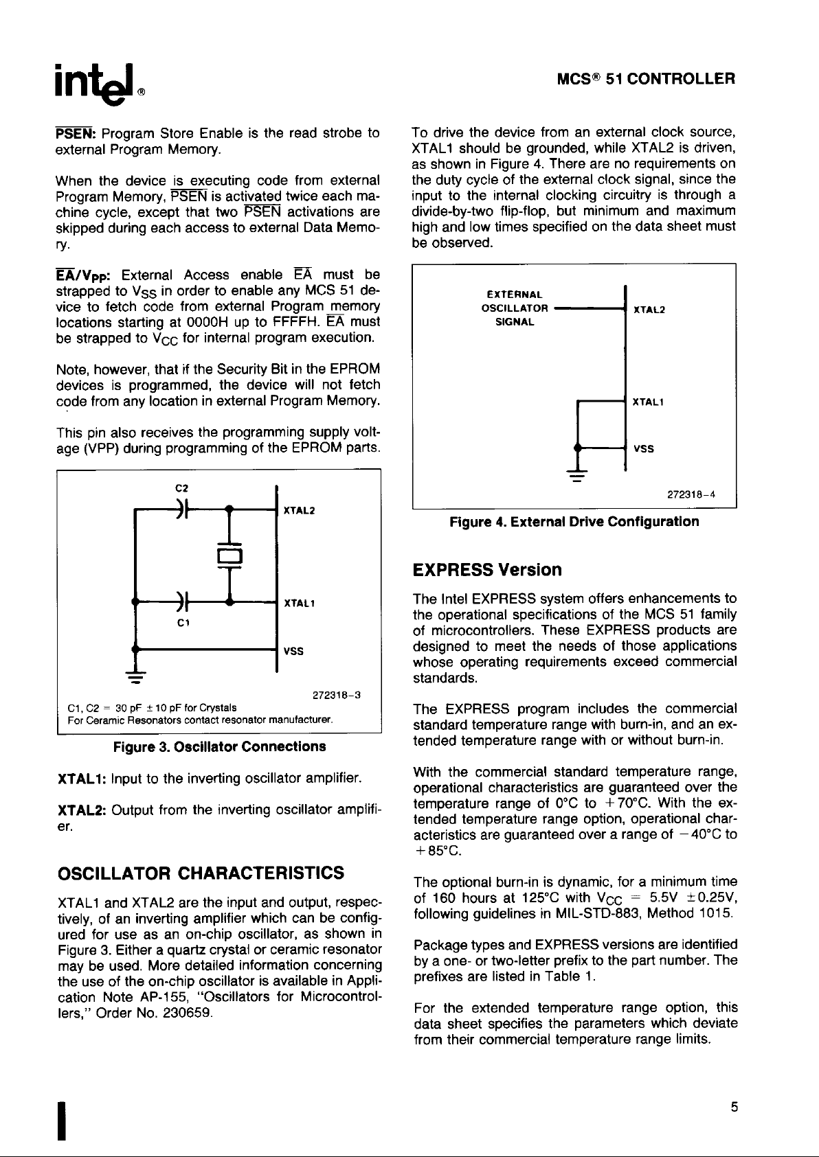
C2
I
El
XTAL2
n
XTAL1
cl
Vss
=
272318-3
Cl, C2 = 30 PF +10 PFfor Crystals
ForCeramic Resonatorscontactresonatormanufacturer.
Figure 3. Oscillator Connections
XTAL1: Input to the inverting oscillator amplifier.
XTAL2: Output from the inverting oscillator amplifi-
er,
OSCILLATOR CHARACTERISTICS
XTAL1 and XTAL2 are the input and output, respectively, of an inverting amplifier which can be configured for use as an on-chip oscillator, as shown in
Figure 3. Either a quartz crystal or ceramic resonator
may be used. More detailed information concerning
the use of the on-chip oscillator is available in Application Note AP-155; “Oscillators
Iers,” Order No, 230659.
I
for Microcontrol-
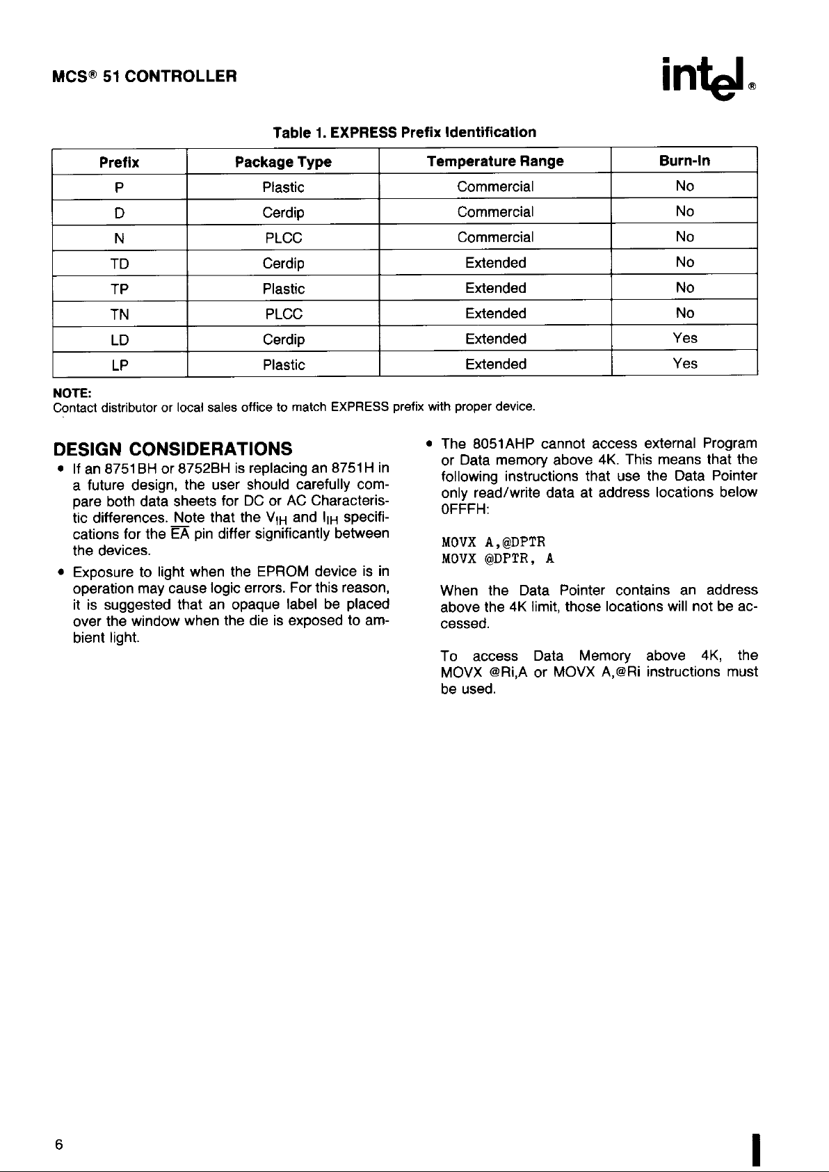
To drive the device from an external clock source,
XTAL1 should be grounded, while XTAL2 is driven,
as shown in Figure 4. There are no requirements on
the duty cycle of the external clock signal, since the
input to the internal clocking circuitry is through a
divide-by-two flip-flop, but minimum and maximum
high and low times specified on the data sheet must
be observed.
EXTERNAL
OSCILLATOR
SIGNAL
XTAL2
XTAL1
Vss
272318-4
Figure 4. External Drive Configuration
EXPRESS Version
The Intel EXPRESSsystem offers enhancements to
the operational specifications of the MCS 51 family
of microcontrollers. These EXPRESS products are
designed to meet the needs of those applications
whose operating requirements exceed commercial
standards.
The EXPRESS program includes the commercial
standard temperature range with burn-in, and an extended temperature range with or without burn-in.
With the commercial standard temperature range,
operational characteristics are guaranteed over the
temperature range of O“C to + 70”C. With the extended temperature range option, operational characteristics are guaranteed over a range of –40”C to
+ 85”C.
The optional burn-in is dynamic, for a minimum time
of 160 hours at 125°C with VCC = 5.5V * 0.25V,
following guidelines in MIL-STD-883, Method 1015.
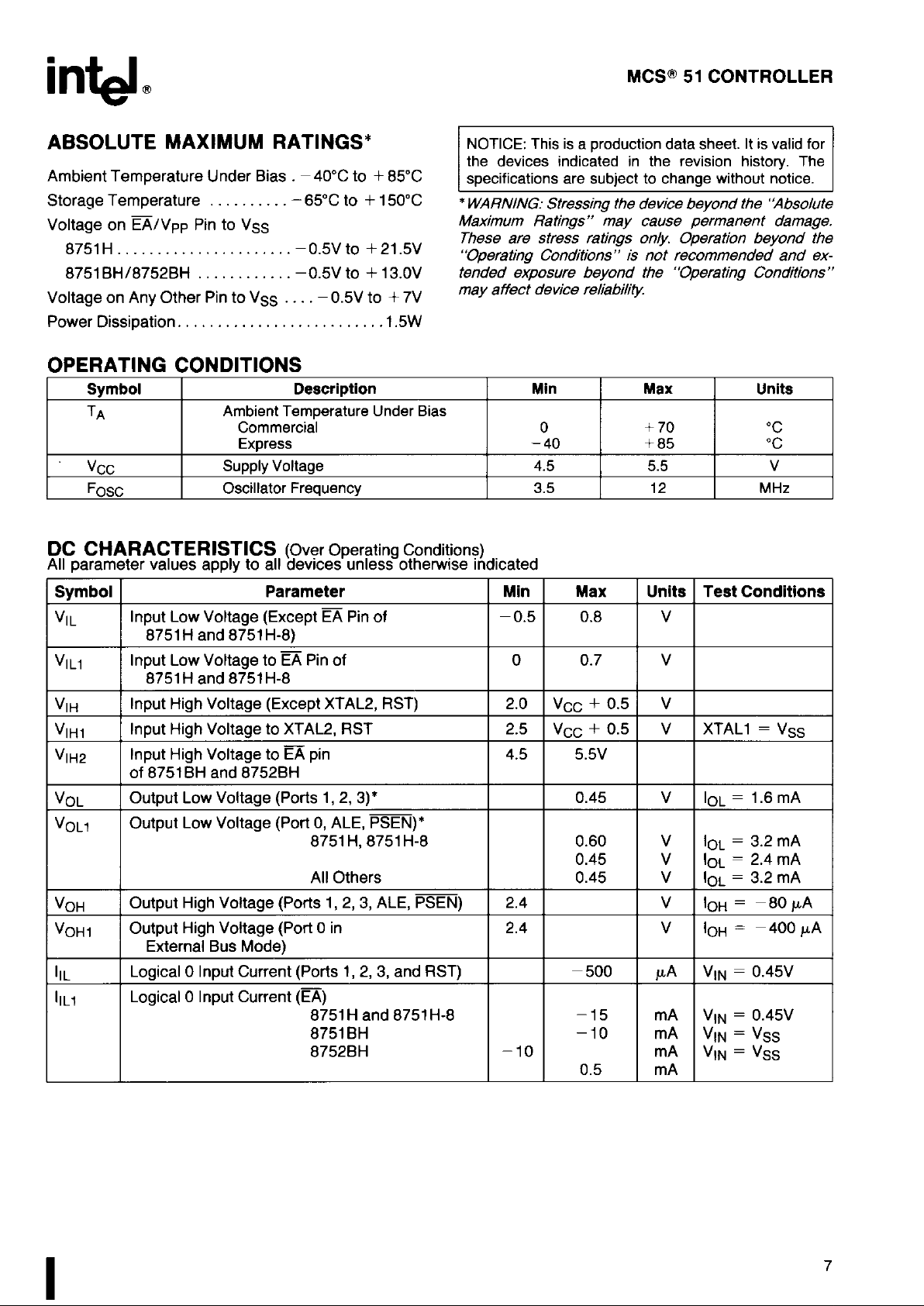
Package types and EXPRESSversions are identified
by a one- or two-letter prefix to the part number. The
prefixes are listed in Table 1.
For the extended temperature range option, this
data sheet specifies the parameters which deviate
from their commercial temperature range limits.
5
Page 6
MCS@51 CONTROLLER
Table 1.EXPRESSPrefix Identification
Prefix Package Type
Temperature Range
Burn-In
P Plastic
Commercial
No
D Cerdip Commercial
No
N PLCC Commercial
No
TD Cerdip Extended
No
TP Plastic Extended No
TN
PLCC Extended No
LD Cerdip Extended
Yes
LP Plastic Extended
Yes
NOTE:
Contactdistributoror localsalesofficeto matchEXPRESSprefixwithproperdevice.
DESIGN CONSIDERATIONS
If an 8751BH or 8752BH is replacing an 8751H in
a future design, the user should carefully compare both data sheets for DCor AC Characteris-
tic differences. Note that the VIH and IIHspecifi-
cations for the ~ pin differ significantly between
the devices.
Exposure to light when the EPROM device is in
operation may cause logic errors. For this reason,
it is suggested that an opaque label be placed
over the window when the die is exposed to ambient light.
●
The 8051AHP cannot access external Program
or Data memory above 4K. This means that the
following instructions that use the Data Pointer
only read/write data at address locations below
OFFFH:
MOVX A,@DPTR
MOVX (6JDPTR,A
When the Data Pointer contains an address
above the 4K limit, those locations will not be accessed.
To access Data Memory above 4K, the
MOVX @Ri,Aor MOVX A,@Ri instructions must
be used.
6
Page 7
MCS” 51 CONTROLLER
ABSOLUTE MAXIMUM RATINGS*
Ambient Temperature Under Bias –40”C to + 85°C
Storage Temperature . –65°C to + 150°C
Voltage on EA/Vpp Pin to Vss
8751H . . . . . . . . . . . . . .. . . –0.5V to + 21.5V
8751BH/6752BH –0.5V
tO + 13.OV
Voltage on Any Other Pinto Vss . –0.5V to + 7V
Power Dissipation. . . ... 1.5W
OPERATING CONDITIONS
NOTICE:This is a productiondatasheet.It is validfor
the devices indicated in the revision history. The
specificationsare subjectto changewithout notice.
*WARNING:
Stressing the device beyond the “Absolute
Maximum Ratings” may cause permanent damage.
These are stress ratings orr~. Operation beyond the
“Operating Conditions” is not recommended and extended exposure beyond the “Operating Conditions”
may affect device reliabili~.
Symbol Description Min
Msx
Units
TA
Ambient Temperature Under Bias
Commercial o
+70
“c
Express –40 +65 “c
Vcc SupplyVoltage
4.5
5.5
v
Fosc
OscillatorFrequency
3.5 12 MHz
DC CHARACTERISTICS (OverOperating Conditions)
All parameter values apply to all devices unless otherwise indicated
Symbol
Parameter Min Max Units Test Conditions
VIL Input Low Voltage (Except~ Pin of –0.5 0.8 v
6751H and 8751H-8)
VIL1 Input Low Voltage to ~ Pinof o 0.7
v
6751H and 8751H-8
VIH Input High Voltage (Except XTAL2, RST) 2.0 Vcc + 0.5 v
VIH1 Input High Voltage to XTAL2, RST 2.5 Vcc + 0.5 v XTAL1 = Vss
VIH2 Input High Voltage to ~ pin 4.5 5.5V
of 6751BHand 8752BH
VoL Output Low Voltage (Ports 1,2, 3)*
0.45 v loL = 1.6 mA
VoLl
Output Low Voltage (Port O,ALE, PSEN)*
8751H, 8751H-8 0.60
v ioL = 3.2 mA
0.45 v !OL= 2.4 mA
All Others 0.45
v IOL= 3.2 mA
VOH Output High Voltage (Ports 1,2,3, ALE, PSEN)
2.4 v IOH= –80 PA
VOH1 Output High Voltage (Port Oin
2.4 v IOH= –400 pA
External Bus Mode)
IIL Logical OInput Current (Ports 1,2,3, and RST) –500
pA
VIN = 0.45V
IILI
Logical OInput Current (~)
8751H and 8751H-8
–15 mA VIN = 0.45V
8751BH –lo mA VIN = Vss
8752BH
–lo mA VIN = Vss
0.5 mA
7
Page 8

MCS” 51 CONTROLLER
DC CHARACTERISTICS
(Over Operating Conditions)
All oarameter values armlv to all devices unless otherwise indicated (Continued)
~—.-...—.—.
_r r.,.-.
Symbol Parameter
Min
Max
Units
Teat Conditions
11L2
Logical OInput Current (XTAL2) –3.2
mA
VIN = 0.45V
ILI Input Leakage Current (Porf O)
8751H and 8751H-8
* 1or)
pA 0.45< VIN < VCC
All Others
t 10
pA 0.45< VIN < VCC
IIH
Logical 1 Input Current (~)
8751H and 8751H-8
500 pA VIN= 2.4V
8751BH/8752BH
1
mA 4.5V < VIN < 5.5V
IIH1 Input Current to RSTto Activate Reset 500
pA
VIN < (Vcc – 1.5V)
Icc Power Supply Current:
8031AH/8051 AH/8051AHP 125
mA
All Outputs
8032AH/8052AH/8751 BH/8752BH 175
mA
Disconnected;
8751H/8751 H-8 250
mA
m = Vcc
Clo PinCapacitance
10
pF Test freq = 1 MHz
NOTES:
1. Capacitive loading on PortsOand 2 may csuse spurious noise pulses to be superimposed on the VOLS of ALE/PROG
and Ports 1 and 3. The noise is
dueto externalbuscapacitancedischargingintothePortOandPort2pinswhenthesepins
make1-to-Otransitionsduringbusoperations.In the worstcases(capacitiveloading> 100pF), the noisepulseon the
ALE/PROGpinmayexceed0.8V.Insuchcasesitmaybedesirableto qualifyALEwitha SchmittTrigger,oruseanaddress
latchwitha Schmi~TriggerSTROBEinput.
2,ALE/PROGrefersto a pinon the 8751BH.ALErefersto a timingsignalthatisoutputontheALE/PROGpin.
3. Understeadystate(non-transient)conditions,loLmustbe externallylimitedasfollows:
MaximumloL perportpin:
10mA
MaximumloLper8-bitpori -
Porto:
26 mA
Ports1,2,and3:
15mA
Maximumtotal toLfor alloutputpins: 71 mA
If loL exceedsthetestcondition,VOLmayexceedtherelatedspecification.Pinsare notguaranteedto sink currentgreater
thanthe listedtestconditions.
8
Page 9

MCS@51 CONTROLLER
EXPLANATION OF THE AC SYMBOLS
Each timing symbol has 5 characters. The first character is always a ‘T’ (stands for time). The other
characters, depending on their positions, stand for
the name of a signal or the logical status of that
signal. The following is a list of all the characters and
what they stand for.
A: Address
C: Clock
D: Input Data
H: Logic level HIGH
1:Instruction (program memory contents)
L: ~level LOW, or ALE
P: PSEN
Q: Output data
R: ~ signal
T: Time
V: Valid
W: WR signal
X: No longer a valid logic level
Z: Float
For example,
TAVLL = Time from Address Valid to ALE Low.
TLLPL = Time from ALE Low to PSEN Low.
AC CHARACTERISTICS (Under Operating Conditions; Load Capacitance for Port O,ALE/PROG, and
PSEN = 100 pF; Load Capacitance for All Other Outputs = 80 pF)
EXTERNAL PROGRAM MEMORY CHARACTERISTICS
Symbol
Parameter
12 MHz Oscillator Variable Oscillator
Units
Min
Max
Min
Max
1/TCLCL Oscillator Frequency
3.5
12.0
MHz
TLHLL ALE PulseWidth
127 2TCLCL–40 ns
TAVLL Address Valid to ALE Low
43 TCLCL–40 ns
TLLAX
Address Hold after ALE Low 48 TCLCL–35
ns
TLLIV
ALE Low to Valid Instr In
8751H
183
4TCLCL– 150
ns
All Others
233 4TCLCL– 100
ns
TLLPL
ALE
LOW to PSENLOW 58 TCLCL–25
ns
TPLPH PSEN PulseWidth
8751H
190 3TCLCL–60
ns
All Others
215
3TCLCL–35
ns
TPLIV
PSENLow to Valid Instr In
8751H
100 3TCLCL– 150
ns
All Others
125 3TCLCL– 125
ns
TPXIX
Input Instr Hold after PSEN
o 0
ns
TPXIZ Input Instr Float after PSEN 63
TCLCL–20
ns
TPXAV
PSENto Address Valid 75 TCLCL–8
ns
TAVIV
Address to Valid Instr In
8751H
287 5TCLCL–1 50
ns
All Others
302 5TCLCL–1 15
ns
TPLAZ
PSEN Low to Address Float 20
20
ns
TRLRH
~ Pulse Width
400
6TCLCL– 100
ns
TWLWH
WR Pulse Width
400
6TCLCL– 100
ns
TRLDV ~ Low to Valid Data In
252 5TCLCL– 165
ns
TRHDX Data Hold after ~
o 0
ns
TRHDZ Data Float after ~
97
2TCLCL–70
ns
TLLDV ALE Low to Valid Data In
517
8TCLCL–1 50
ns
-.. .. .. . , , .,–,. , -—.—,.–
.,. -
nl-n, n, .ec
--
I AVUV
I
Aaaress 10valla Ua[a m
I
I
DUD
I I
Y
I ~LUL— 103
I
rm
9
Page 10

MCS@51 CONTROLLER
EXTERNAL PROGRAM MEMORY CHARACTERISTICS
(Continued)
Symbol
TLLWL
TAVWL
TQVWX
TQVWH
TWHQX
TRLAZ
TWHLH
‘arame’erI---%#
ALE Low to RDor WR Low 200
Address to ~ or WR Low 203
Data Valid to WR Transition
8751H
I
13
All Others
23
Data Valid to WR High
433
Data Hold after WR
33
RD Low to Address Float
RDor WR High to ALE High
8751H
33
All Others 43
cillator VariableOscillator
Units
Max
Min
Max
300 3TCLCL–50
3TCLCL+ 50 ns
4TCLCL– 130
ns
TCLCL–70 ns
TCLCL–60
ns
7TCLCL– 150
ns
TCLCL–50 ns
20 I I 20 I ns I
133 TCLCL–50
TCLCL+ 50 ns
123 TCLCL–40 TCLCL+40 ns
NOTE:
“The 8751H-8 is identicalto the 8751Hbut only o~eratesutI to 8 MHz.Whencalculatingthe AC Characteristicsfor the
8751 H-8, use the 8751 H formula for variable oscillators.
10
Page 11

MCS@51 CONTROLLER
EXTERNAL PROGRAM MEMORY READ CYCLE
w--- TLHLL _
ALE
\ ,
/
\
TLLPL- ~ TPLPH
-TAVLL+ + TLLIV
PSEN
/
TLLAX
PORTO
1
PORT2
x
AO
-A15
x
A8 -A15
272318-5
EXTERNAL DATA MEMORY READ CYCLE
ALE
Y
\
/
+TLHLL+
TWHLH
PSEN
‘LLOv ~
— TLLWL
TRLRH –—
m
+
TAVLL
+
b i ‘
_TLLAX
—TRLDV4
TRHOX+
PORTO
AO-A7 FROM RI OR OPL OATAIN
.
.
TAVOV b
PORT2
x r
P2.O-P2.7 OR A8-A15 FROMDPH
x
A8-A15 FROMPCH
272318-6
EXTERNAL DATA MEMORY WRITE CYCLE
ALE
\ ,
\
/
TLHLL—
TWHLH
m
/
‘TLLwL~TwLwH
*
WT
1
TAVLL
k
1 ‘
+TLLAX
7t=-
TQVWX
: r
TWHQX
TQVWH
II I 1
PORTO
AO-A7
FROMRIOROPL
M
OATAOUT
xx
AO-A7 FROMFCL
I
PORT2
x
P2.O-P2.7 OR A8-A15 FROMOPH
x
A8-A15 FROMPCH
272318-7
11
Page 12

M=” 51 CONTROLLER
SERIAL PORT TIMING—SHIFT
Test Conditions: Over ODeratina Conditions: Load Capacitance = 80 rJF
Symbol
TXLXL
TQVXH
TXHQX
TXHDX
TXHDV
Parameter
12 MHz Oscillator VariableOscillator
Unite
Min
Max
Min Max
Serial Port Clock CycleTime
1.0 12TCLCL ps
Output Data Setup to Clock Rising
700 1OTCLCL– 133 ns
Edge
Output Data Hold after Clock
50 2TCLCL–1 17
ns
Rising Edge
Input Data Hold after Clock Rising
o
0
ns
Edge
Clock Rising Edge to Input Data 700
10TCLCL– 133 ns
Valid
;HI17REGISTERMODETIMINGWAVEFORMS
INSTRUCTION I O I 1 I 2 I 3 I 4 I 5 I 6 I 7 I 8 I
ALE
n n
n n n n n n n
n
n n n n n n n n
I
I-TXLXL-7
CLOCK
WI-TXHQX I
OUTPUTOATA
o 1)( 1 2
x
3
x
4
x
5
x
6
x
7
/
,
+
SET TI
INPUT DATA
~
4
SET RI
272318-8
12
Page 13

MCS@51 CONTROLLER
EXTERNAL CLOCK DRIVE
Symbol Parameter Min Max
Units
1
1/TCLCL Oscillator Frequency (except 8751H-8) 3.5 12 MHz
8751H-8 3.5
8
MHz
TCHCX
High Time
20 ns
TCLCX
Low Time
20 ns
I TCLCH I Rise Time
I I 20 I ns I
TCHCL
Fall Time 20 ns
EXTERNAL CLOCK DRIVE WAVEFORM
— TCHCX —
TCLCH _
—
—
~ TCliCL
2.5
t
a
t 2.5
A
-— TCLCX —
+
TCLCL
w
272318-9
AC TESTING INPUT, OUTPUT WAVEFORM
2.4
2.0 2.0
><
TEST POINTS
0.s 0.8
0.45
272318-10
AC Testing: Inputsare driven at 2.4V for a Logic“1” and 0.45V
for a Logic “O”. Timing measurements ara made at 2.OV for a
Logic“1” and 0.8V for a Logic“O”.
Page 14

MCS@51 CONTROLLER
EPROM CHARACTERISTICS
Table3.EPROMProgrammingModea
Mode RST
PSEN
ALE m P2.7 P2.6 P2.5
P2.4
Program
1 0
o*
VPP
1 0
x
x
Verify
1 0
1 1 0 0
x
x
Security Set
1 0
o*
VPP
1
1 x
x
NOTE:
“1” = logichighfor that pin
“O” = logiclowfor thatpin
“X” = “don’tcare”
PROGRAMMING THE 8751H
To be programmed, the part must be running with a
4 to 6 MHz oscillator. (The reason the oscillator
needs to be running is that the internal bus is being
used to transfer address and program data to appropriate internal registers.) The address of an EPROM
location to be programmed is applied to Port 1 and
pins P2.O-P2.3 of Port 2, while the code byte to be
programmed into that location is applied to Port O.
The other Porl 2 pins, and RST, PSEN,and ~/Vpp
should be held at the “Program” levels indicated in
Table 3. ALE/PROG is pulsed low for 50 ms to program the code byte into the addressed EPROM location. The setup is shown in Figure 5.
Normally ~~is held at a logic highflntil just
before ALE/PROG is to be pulsed. Then EA/Vpp is
raised to +21 V, ALE/PROG is pulsed, and then
~/Vpp is returned to a logic high. Waveforms and
detailed timing specifications are shown in later sections of this data sheet.
+5V
a
Vcc
AOOR
A&b? p?
—FFH
w
PGM DATA
P2.0–
U–All
P2.3
8751H
‘=’’-”TCAREJ=E‘LEl=$=-
U
Vlli P2.7
XTAU
5
F&vPP
4-SUN* n
XTAL1
RST
VIH1
Vss
PSEN
.
.
27231a-1 I
Figure5.ProgrammingConfiguration
“VPP” = +21V *0.5V
*ALEis pulsedlowfor 50 ms
Note that the ~/VPP pin must not be allowed to go
above the maximum specified VPP level of 21.5Vfor
any amount of time. Even a narrow glitch above that
voltage Ievei can cause permanent damage to the
device. The VPP source should be well regulated
and free of glitches.
Program Verification
If the Security Bit has not been programmed, the onchip Program Memory can be read out for verification purposes, if desired, either during or after the
programming operation. The address of the Program
Memory location to be read is appiied to Port 1 and
pins P2.O-P2.3. The other pins should be held at the
“Verify” Ieveis indicated in Tabie 3. The contents of
the addressed location will come out on Port O.External pullups are required on Port Ofor this operation.
The setup, which is shown in Figure 6, is the same
as for programming the EPROMexcept that pin P2.7
is held at a logic low, or may be used as an activeIow read strobe
+5V
?
Vcc
mu
w +
DATA
—FFH
(USE 10K
PULLUPS]
W51H
x
~ . ,,W,, CARE,. - ~~b
X-9
P2.5 ALE
VIL d P2.S
VIH
ENAS4E
. P2 7
G
J-
XTAU
4-6 MHZm
RST h VIH1
XTAL1
Vss
PSEN
.
27231S-12
Figure6.ProgramVerification
14
Page 15

MCS@51 CONTROLLER
EPROM Security
The security feature consists of a ‘locking” bit which
when programmed denies electrical access by any
external means to the on-chip Program Memory.
The bit is programmed as shown in Figure 7. The
setup and procedure are the same as for normal
EPROM programming, except that P2.6 is held at a
logic high, Porl O,Port 1 and pins P2.O–P2.3may be
in any state. The other pins should be held at the
“Security” levels indicated in Table 3.
Once the Security Bit has been programmed, it can
be cleared only by full erasure of the Program Memory. While it is programmed, the internal Program
Memory can not be read out, the device can not be
further programmed, and it
cannotexecuteoutof
externalprogrammemory.
Erasing the EPROM,
thus clearing the Security Bit, restores the device’s
full functionality. It can then be reprogrammed.
+5V
X = OGN’T CARE”
o
f
Vcc
{:
‘-
PI
m x
P2.0-
X
P2.3
8751H
P2.4
ALE
ALE/PROO
P2.5
50 ma PULSE TO GND
P2.6
VIM
P2,7
fi
+ EAYPP
XTAU
m
RST
— WH1
XTAL1
Vss
PSEN
7
*
*
272318-13
Erasure Characteristics
Erasure of the EPROM begins to occur when the
device is exposed to light with wavelengths shorter
than approximately 4,000 Angstroms. Since sunlight
and fluorescent lighting have wavelengths in this
range, exposure to these light sources over an extended time (about 1 week in sunlight, or 3 years in
room-level fluorescent lighting) could cause inadvertent erasure. If an application subjects the device to
this type of exposure, it is suggested that an opaque
label be placed over the window.
Figure7.ProgrammingtheSecurityBit
The recommended erasure procedure is exposure
to ultraviolet light (at 2537 Angstroms) to an integrated dose of at least 15 W-sec/cm2. Exposing the
EPROM to an ultraviolet lamp of 12,000 pW/cm2
rating for 20 to 30 minutes, at a distance of about
1 inch, should be sufficient.
Erasure leaves the array in an all 1‘s state.
EPROM PROGRAMMING AND VERIFICATION CHARACTERISTICS
TA = 21°C to 27”C; VCC = 5V + 10%; VSS = OV
Symbol
Parameter Min
Max
Unita
VPP
Programming Supply Voltage
20.5
21.5
v
IPP
Programming Supply Current 30 mA
1/TCLCL Oscillator Frequency
4 6
MHz
TAVGL Address Setup to PROG Low 46TCLCL
TGHAX
Address Hold after PROG
48TCLCL
TDVGL Data Setup to PROG Low 48TCLCL
TGHDX
Data Hold after~ 48TCLCL
TEHSH
P2.7 (ENABLE) High to VPP 48TCLCL
TSHGL VPPSetup to PROGLow 10
ps
TGHSL
VPP Hold after PROG
10
ps
TGLGH
PROGWidth 45 55
ms
TAVQV
Address to Data Valid 48TCLCL
TELQV
ENABLE Low to DataValid 48TCLCL
TEHQZ
Data Float after ENABLE
o
48TCLCL
15
Page 16

MCS” 51 CONTROLLER
GI-” ”nl r“”” ”mrnmrlmn. w I-8. ” ,Lrl.. .“4-s . m“.. ..-. b. “..8.,”
PROGRAMMING VERIFICATION
P1.O-PI.7
P3,0-P3,3
(
ADDRESS
$ J
—
PORTO
{ ,
DATAIN
TOVGL — —
—TGHOX
TAVGL
— TGHAX
kLE/PROG
\ ~ ‘
TSHGL
— —
—
TGHSL
TGLGH
21V * .5V
r
\
m HIGH
Fi.vPP
TTLHIGH
TTLHIGH
TSHSN
— TELOV
P3.7
(ENABLE)
1 ‘
\
272318-14
For programmingconditionssee Figure5.
For verificationconditionssee Figure 6.
16
Page 17

inlA
MCS” 51 CONTROLLER
Programming the 8751BH/8752BH
To be programmed, the 875XBH must be running
with a 4 to 6 MHz oscillator. (The reason the oscillator needs to be running is that the internal bus is
being used to transfer address and program data to
appropriate internal registers.) The address of an
EPROM location to be programmed is applied to
Porl 1 and pins P2.O- P2.4 of Port 2, while the code
byte to be programmed into that location is applied
to Port O. The other Port 2 and 3 pins, and RST,
PSEN,and ~/Vpp should be held at the “Program”
levels indicated in Table 1.ALE/PROG is pulsed low
to croaram the code bvte into the addressed
Normally ~&is held at a logic high until just
before ALE/PROG is to be pulsed. Then ~/Vpp is
raised to Vpp, ALE/PROG is pulsed low, and then
~/Vpp is returned to a valid high voltage. The voltage on the ~/Vpp pin must be at the valid EA/Vpp
high level before a verify is attempted. Waveforms
and detailed timing specifications are shown in later
sections of this data sheet.
Note that the ~/Vpp pin must not be allowed to go
above the maximum specified Vpp level for any
amount of time. Even a narrow glitch above that voltage level can cause permanent damage to the device. The Vpp source should be well regulated and
EPROfl location. The setu’p is shown in Figure 8.
free of glitches.
+5V
Vcc
Po
1
~ RST
E/vpp
~
+12.75V
ALE/PROG
~25 100 p, PULSESTOGND
1
~ P3.6
875X,, ~
~“
1
~ P3.7
P2.7
~1
lJ-
XTAL2
P2.6 ~o
4-6 MHz
❑
T= ;
XTAL1
P2.O
-P2,4
‘ks
=
272318-15
—. —
Figure8.Programmingthe EPROM
Table4.EPROMProgrammingModeafor875XBH
MODE
RST
ALE/
PSEN —
ml
PROG
Vpp
P2.7 P2.6
P3.6 P3.7
Program Code Data 1
0
o*
Vpp 1 0 1 1
Verify Code Data 1 0
1
1 0 0 1 1
Program Encryption Tabie 1
0
o*
Vpp 1 0
0
1
Use Addresses O-1FH
Program Lock
~= 1
1 0 o*
Vpp 1 1 1 1
Bits (LBx) x=2 1 0 o*
Vpp 1
1
0 0
Read Signature 1
0
1
1 0 0
0 0
NOTES:
“1” = Validhighforthatpin
“O” = Validlowfor that pin
“vpp”
= +12.75V+0.25V
*ALE/PROGispulsedlowfor 100USforprogramming.(Quick-PulseProgramming)
17
Page 18

MCS@51 CONTROLLER
QUICK-PULSE PROGRAMMING
ALGORITHM
The 875XBH can be programmed using the QuickPulse Programming Algorithm for microcontrollers.
The features of the new programming method are a
lower Vpp (12.75 volts as compared to 21 volts) and
a shorter programming pulse. For example, it is possible to program the entire 8 Kbytes of 875XBH
EPROM memory in less than 25 seconds with this
algorithm!
To program the part using the new~rithm, Vpp
must be 12,75 f 0.25 Volts. ALE/PROG is pulsed
low for 100 pseconds, 25 times as shown in
Figure 9, Then, the byte just programmed may be
verified. After programming, the entire array should
be verified. The Program Lock features are programmed using the same method, but with the setup
as shown in Table 4. The only difference in programming Lock features is that the Lock features cannot
be directly verified. Instead, verification of programming is by observing that their features are enabled.
PROGRAM VERIFICATION
If the Lock Bits have not been programmed, the onchip Program Memory can be read out for verification purposes, if desired, either during or after the
programming operation. The address of the Program
Memory location to be read is applied to Port 1 and
pins P2.O- P2.4. The other pins should be held at
the “Verify” levels indicated in Table 1. The contents of the addressed location will come out on Port
O. External pullups are required on Port O for this
operation. (If the Encryption Array in the EPROM
has been programmed, the data present at Port O
will be Code Data XNOR Encryption Data. The user
must know the Encryption Array contents to manual-
ly “unencrypt” the data during verify.)
The setup, which is shown in Figure 10, is the same
as for programming the EPROMexcept that pin P2.7
is held at a logic low, or may be used as an active
low read strob~.
, ~25p”LsEs ~
ALEM
n--------
I
“
10 P,MIN
100JM
*lops
ALE/PROG:
0
1
272318-16
Figure9.PROGWaveforma
+~v
‘r
h 10kJl
AO-A7 P!
RST
P3.6
1
P3.7
L
XTAL2
4-6 MHz
❑
XTAL1
Vss
=
Vcc
-F’
X8
Po
PGM
DATA
rmpp
ALE/PRW
1
B75xBH = 0
P2.7 0 (i-mm
P2.6
0
P2.O
-P2.4
F
A8-A12
272318-17
Figure10.VerifyingtheEPROM
18
Page 19

PROGRAM MEMORY LOCK
The two-level Program Lock system consists of 2
Lock bits and a 32-byte Encryption Array which are
used to protect the program memory against software piracy.
ENCRYPTION ARRAY
Within the EPROM array are 32 bytes of Encryption
Array that are initially unprogrammed (all 1s). Every
time that a byte is addressed during a verify, 5 address lines are used to select a byte of the Encryption Array. This byte is then exclusive-NORed
(XNOR) with the code byte, creating an Encrypted
Verify byte. The algorithm, with the array in the unprogrammed state (all 1s), will return the code in its
original, unmodified form.
It is recommended that whenever the Encryption Array is used, at least one of the Lock Bits be pro-
grammed as well.
LOCK BITS
Also included in the EPROM Program Lock scheme
are two Lock Bits which function as shown in Table
5.
Erasing the EPROM also erases the Encryption Ar-
ray and the Lock Bits, returning the part to full unlocked functionality.
MCS@51 CONTROLLER
Table5.LockBitsandtheirFeatures
LogicEnabled
LB1
u
=
Minimum Program Lock features
enabled. (Code VerifyWIIIstill be
P u
MOVC instructions executed from
external program memory are
disabled from fetching code bytes
from internal memory, EA is
sampled and latched on reset,
and further programming of the
EPROMis disabled
P
I
P
Same as above, but Verify is also
disabled
U
I P IReservedfor Future Definition I
= Programmed
= Unprogrammed
READING THE SIGNATURE BYTES
The signature bytes are read by the same procedure
as a normal verification of locations 030H and 031H,
except that P3.6 and P3.7 need to be pulled to a
logic low. The values returned are:
(030H) = 89H indicates manufactured by Intel
(031H) = 51H indicates 8751BH
52H indicates 8752BH
To ensure proper functionality of the chip, the internally latched value of the ~ pin must agree with its
external state.
19
Page 20

MCS” 51 CONTROLLER
ERASURE CHARACTERISTICS
Erasure of the EPROM begins to occur when the
8752BH is exposed to light with wavelengths shorter
than approximately 4,000 Angstroms. Since sunlight
and fluorescent lighting have wavelengths in this
range, exposure to these light sources over an extended time (about 1 week in sunlight, or 3 years in
room-level fluorescent lighting) could cause inadvertent erasure. If an application subjects the device to
this type of exposure, it is suggested that an opaque
label be placed over the window.
The recommended erasure procedure is exposure
to ultraviolet light (at 2537 Angstroms) to an integrat-
ed dose of at lease 15 W-see/cm. Exposing the
EPROMto an ultraviolet lamp of 12,000 pW/cm rat-
ing for 30 minutes, at a distance of about 1 inch,
should be sufficient.
Erasure leaves the array in an all Is state.
EPROM PROGRAMMING AND VERIFICATION CHARACTERISTICS
(T,4 = 21°C to 27”C, Vcc = 5.OV + 10%, Vss = OV)
Symbol
Parameter
Min
Max Units
Vpp
Programming Supply Voltage 12.5
13.0 v
Ipp
Programming Supply Current
50
mA
1/TCLCL
Oscillator Frequency
4
8 MHz
TAVGL
Address Setup to PROG Low 48TCLCL
TGHAX
Address Hold After PROG
48TCLCL
TDVGL
Data Setup to PROG Low
48TCLCL
TGHDX
Data Hold After PROG
48TCLCL
TEHSH
P2.7 (ENABLE) High to Vpp
48TCLCL
TSHGL
Vpp Setup to PROG Low 10
ps
TGHSL
Vpp Hold After PROG 10
ps
TGLGH
PROGWidth 90
110 ps
TAVQV
Address to Data Valid
48TCLCL
TELQV
ENABLE Lowto Data Valid
48TCLCL
TEHQZ
Data Float After ENABLE
o
48TCLCL
TGHGL
PROGHighto PROGLow 10
ps
EPROM PROGRAMMING AND VERIFICATION WAVEFORMS
PROGRAMMING
VERIFICATION
‘::=&z
~ .-~
}
ADDRESS
ADDRFSS
TAvQV
DATAIN
DATAOUT
TDVGL
TGHDX
TAVGL
Pu& TGHAX
TSHGL
d TGHsL
TGLGH
TGHGL
~wpp
t
[A/HIGH
TELQV L
TEHQZ
P2.7
272318-18
20
Page 21

MCS@51 CONTROLLER
DATA SHEET REVISION HISTORY
Datasheets are changed as new device information becomes available. Verify with your local Intel sales office
that you have the latest version before finalizing a design or ordering devices.
The following differences exist between this datasheet (272318-002) and the previous version (272318-001):
1. Removed QP and QD (commercial with extended burn-in) from Table 1. EXPRESS Prefix Identification.
This datasheet (272318-001) replaces the following datasheets:
MCS@51 Controllers (270048-007)
8051AHP (270279-004)
8751BH (270248-005)
8751BH EXPRESS (270708-001)
8752BH (270429-004)
8752BH EXPRESS (270650-002)
21
 Loading...