

Page 1
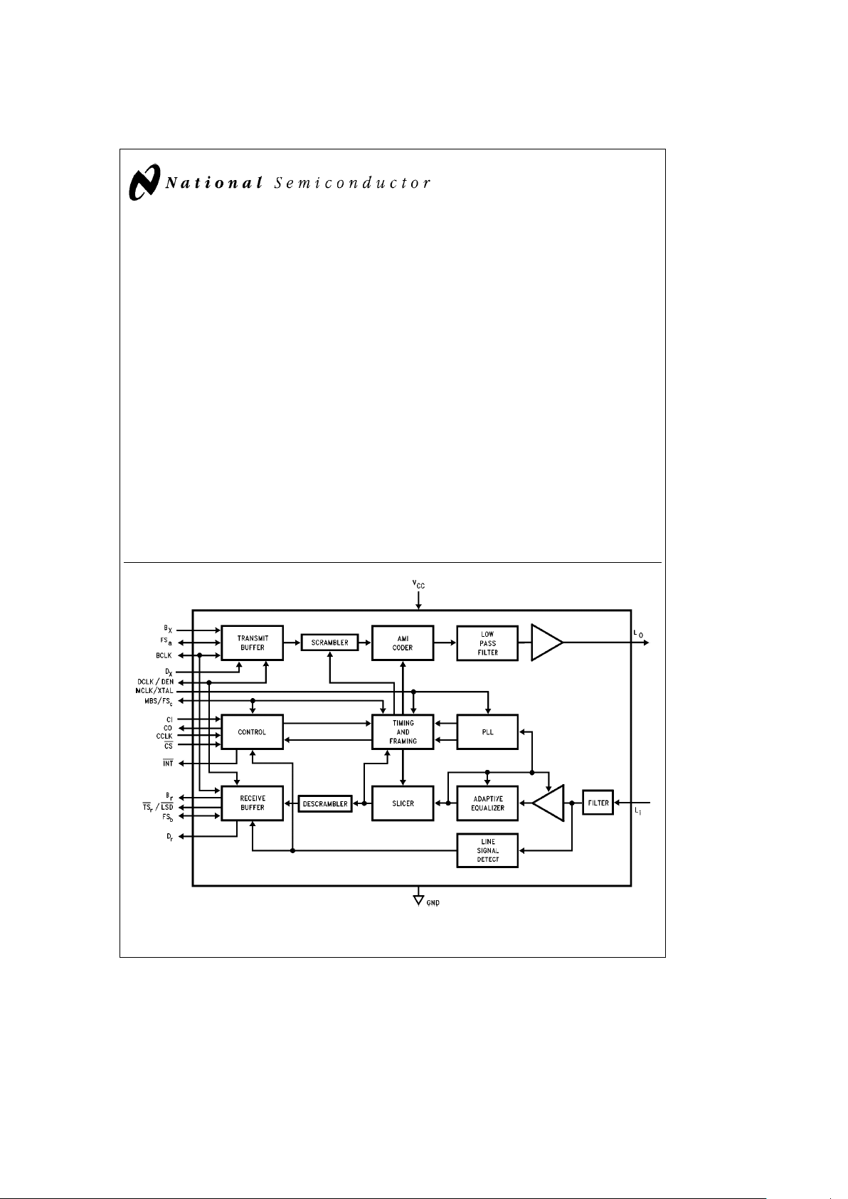
TL/H/11725
TP3406 DASL Digital Adapter for Subscriber Loops
November 1992
TP3406
DASL Digital Adapter for Subscriber Loops
General Description
The TP3406 is a complete monolithic transceiver for data
transmission on twisted pair subscriber loops. It is built on
National’s double poly microCMOS process, and requires
only a single
a
5 Volt supply. Alternate Mark Inversion (AMI)
line coding, in which binary ‘1’s are alternately transmitted
as a positive pulse then a negative pulse, is used to ensure
low error rates in the presence of noise with lower emi radiation than other codes such as Bi-phase (Manchester).
Full-duplex transmission at 144 kb/s is achieved on a single
twisted wire pair using a burst-mode technique (Time Compression Multiplexed). Thus the device operates as an ISDN
‘U’ Interface for short loop applications, typically in a PBX
environment, providing transmission for 2 B channels and 1
D channel. On
Ý
24 cable, the range is up to 800 meters.
System timing is based on a Master/Slave configuration,
with the line card end being the Master which controls loop
timing and synchronisation. All timing sequences necessary
for loop activation and de-activation are generated on-chip.
Selection of Master and Slave mode operation is programmed via the Microwire Control Interface.
A 2.048 MHz clock, which may be synchronized to the system clock, controls all transmission-related timing functions.
Features
Complete ISDN PBX 2-Wire Data Transceiver including:
Y
2 B plus D channel interface for PBX UÊInterface
Y
144 kb/s full-duplex on 1 twisted pair using Burst Mode
Y
Loop range up to 800 meters (Ý24AWG)
Y
Alternate Mark Inversion coding with transmit filter and
scrambler for low emi radiation
Y
Adaptive line equalizer
Y
On-chip timing recovery, no external components
Y
Standard TDM interface for B channels
Y
Separate interface for D channel
Y
2.048 MHz master clock
Y
Driver for line transformer
Y
4 loop-back test modes
Y
Singlea5V supply
Y
MICROWIRETMcompatible serial control interface
Y
Applications in:
PBX Line Cards
Terminals
Regenerators
Y
Available in 28-pin PLCC Package
Block Diagram
TL/H/11725– 1
TRI-STATEÉis a registered trademark of National Semiconductor Corporation
MICROWIRE
TM
is a trademark of National Semiconductor Corporation.
C
1995 National Semiconductor Corporation RRD-B30M115/Printed in U. S. A.
Page 2
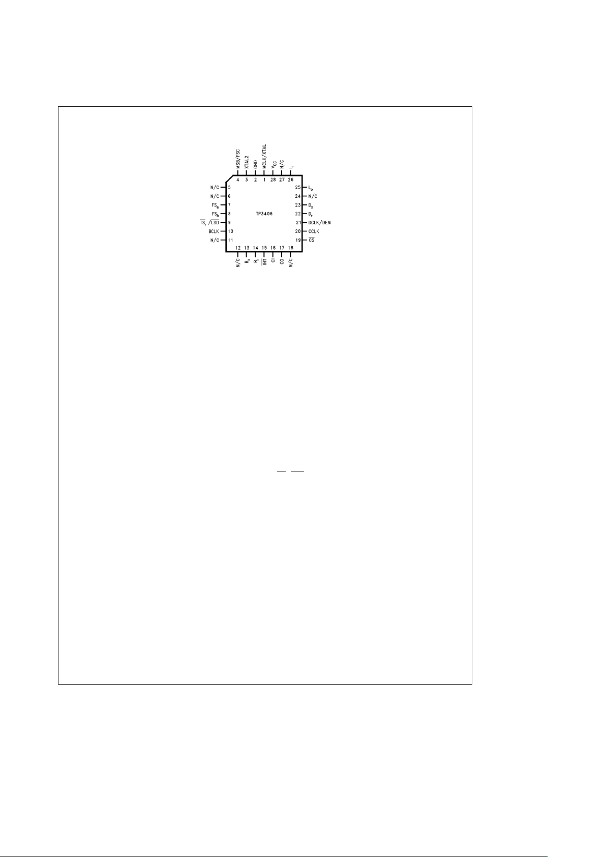
Connection Diagram
TP3406 Package Information
TL/H/11725– 2
Order Number TP3406V
See NS Package Number V28A
Pin Descriptions
Name Description
GND Negative power supply pin, normally 0V. All
analog and digital signals are referred to this
pin.
V
CC
Positive power supply input, which must be
a
5Vg5%.
MCLK The 2.048 MHz Master Clock input, which
requires a CMOS logic level clock input from
a stable source. Must be synchronous with
BCLK.
MCLK/XTAL This pin is the 2.048 MHz Master Clock in-
put, which requires either a crystal to be connected between this pin and XTAL2 or a
CMOS logic level clock from a stable source,
which must be synchronous with BCLK.
XTAL2 This pin is the output side of the oscillator
amplifier.
MBS/FS
C
In Master Mode, this pin is the Master Burst
Sync input, which may be clocked at 4 kHz
to synchronize Transmit bursts from a number of devices at the Master end only. The 4
kHz should be nominally a square wave signal. If not used leave this pin open. In Slave
mode, this pin is a short Frame Sync output,
suitable for driving another DASL in Master
Mode to provide a regenerator (i.e. range-extender) capability.
BCLK Bit Clock logic signal which determines the
data shift rate for B channel data on the digital interface side of the device. In Master
mode this pin is an input which may be any
multiple of 8 kHz from 256 kHz to
2.048 MHz, but must be synchronous with
MCLK. In Slave mode this pin is an output at
2.048 MHz.
FS
a
In Master mode only, this pin is the Transmit
Frame Sync pulse input, requiring a positive
edge to indicate the start of the active channel time for transmit B channel data into B
x
;
FS
a
must be synchronous with BCLK and
MCLK. In Slave mode only, this pin is a digi-
Name Description
tal output pulse which indicates the 8-bit periods of the B1 channel data transfer at both
B
x
and Br.
FS
b
In Master mode only, this pin is the Receive
Frame Sync pulse input, requiring a positive
edge to indicate the start of the active channel time of the device for receive B channel
data out from B
r
;FSbmust be synchronous
with BCLK and MCLK. In Slave mode only,
this pin is a digital output pulse which indicates the 8-bit periods of the B2 channel
data transfer at both B
x
and Br.
B
x
Digital input for B1 and B2 channel data to
be transmitted to the line; must be synchronous with BCLK.
B
r
Digital output for B1 and B2 channel data
received from the line.
TS
r
/LSD In Master mode only, this pin is an open-
drain output which is normally high impedance but pulls low during both B channel active receive time slots. In Slave mode only,
this pin is an output which is normally high
impedance and pulls low when a valid line
signal is received.
D
x
Digital input for D channel data to be transmitted to the line; must be synchronous with
DCLK.
D
r
Digital output for D channel data received
from the line. D
r
is a TRI-STATE output.
DCLK/DEN In Master mode this pin is an input for the
16 kHz serial shift clock for D channel data
on D
x
and Dr, which should be synchronous
with BCLK. It may also be re-configured via
the Control Register to act as an enable input for clocking the D channel interface synchronized to BCLK. In Slave mode this is a
16 kHz clock output for D channel data.
*Crystal specifications: 2.048 MHz parallel resonant, R
S
s
100X with a
20 pF load. Crystal tolerance should be
g
75 ppm for aging and tempera-
ture.
2
Page 3
Pin Descriptions (Continued)
Name Description
CI MICROWIRE control channel serial data in-
put.
CO MICROWIRE control channel serial data out-
put.
CCLK Clock input for the MICROWIRE control
channel.
CS
Chip Select input which enables the MICROWIRE control channel data to be shifted in
and out when pulled low. When high, this pin
inhibits the MICROWIRE interface.
INT
Interrupt output, a latched output signal
which is normally high-impedance and goes
low to indicate a change of status of the loop
transmission system. This latch is cleared
when the Status Register is read by the microprocessor.
L
o
Transmit AMI signal output to the line transformer. This pin is capable of driving a load
impedance
t
60X.
L
i
Receive AMI signal input from the line transformer. This is a high impedance input.
Functional Description
POWER-UP/POWER-DOWN CONTROL
Following the initial application of power, the DASL enters
the power-down (de-activated) state, in which all the internal
circuits are inactive and in a low power state except for the
line-signal detect circuit and the necessary bias circuit; the
line output L
o
is in a low impedance state and all digital
outputs are inactive. All bits in the Control Register powerup initially set to ‘0’, so that the device always initializes as
the Master end. Thus, at the Slave end, a control word must
be written through the MICROWIRE port to select Slave
mode. While powered-down, the Line-Signal Detect circuits
in both Master and Slave devices continually monitor the
line, to enable loop transmission to be initiated from either
end.
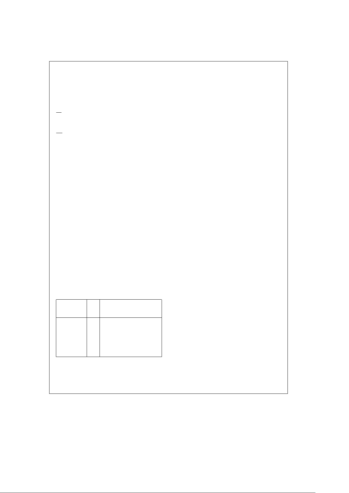
To power-up the device and initiate activation, bit C6 in the
Control Register must be set high. Setting C6 low de-activates the loop and powers-down the device, see Table I.
TABLE I. Master Mode Burst
Sync Control (TP3401 Only)
MBS/FS
c
C6
Pin I/P
State
Action
at Master
Don’t Care 0 Powered-down, Line-Signal
Detect active
Pull up this pin 1 Powered-up, sending bursts
synchronized to FS
a
toa5V through
a resistor
4 kHz 1 Powered-up, sending bursts
synchronized to MBS
LINE TRANSMIT SECTION
Alternate Mark Inversion (AMI) line coding is used on the
DASL because of its spectral efficiency and null dc energy
content. All transmitted bits, excluding the start bit, are
scrambled by a 9-bit scrambler to provide good spectral
spreading with a strong timing content. The scrambler feedback polynomial is:
x
9
a
x
5
a
1.
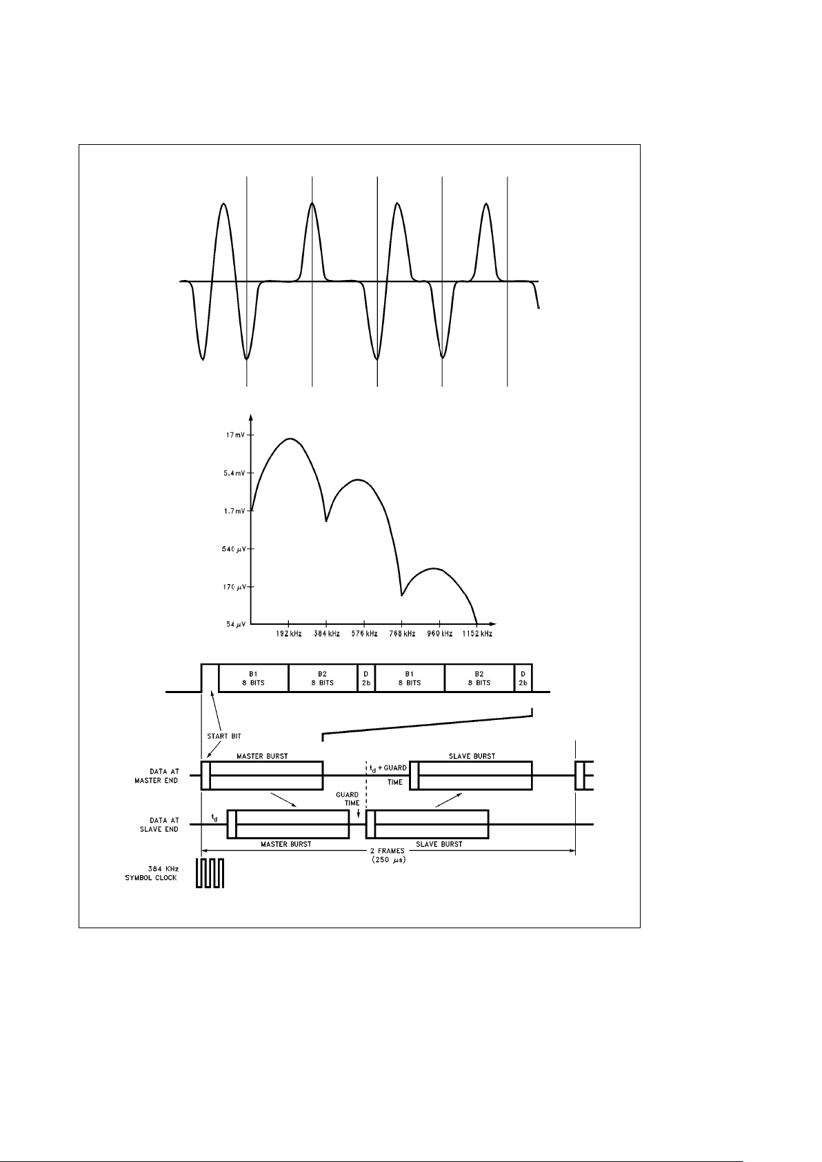
Pulse shaping is obtained by means of a raised cosine
switched-capacitor filter, in order to limit rf energy and
crosstalk while minimizing inter-symbol interference (isi).
Figure 3
shows the pulse shape at the Looutput, while a
template for the typical power spectrum transmitted to the
line with random data is shown in
Figure 4
.
The line-driver output, Lo, is designed to drive a transformer
through a capacitor and termination resistor. A 1:1 transformer, terminated in 100X, results in a signal amplitude of
typically 1.3V pk-pk on the line. Over-voltage protection
must be included in the interface circuit.
LINE RECEIVE SECTION
The front-end of the receive section consists of a continuous anti-alias filter followed by a switched-capacitor lowpass filter designed to limit the noise bandwidth with minimum intersymbol interference. To correct pulse attenuation
and distortion caused by the transmission line an AGC circuit and first-order equalizer adapt to the received pulse
shape, thus restoring a ‘‘flat’’ channel response with maximum received eye opening over a wide spread of cable
attenuation characteristics.
From the equalized output a DPLL (Digital Phase-Locked
Loop) recovers a low-jitter clock for optimum sampling of
the received symbols. The MCLK input provides the reference clock for the DPLL at 2.048 MHz. At the Master end of
the loop this reference is the network clock (BCLK), which
controls all transmit functions; the DPLL clock is used only
for received data sampling. At the Slave end, however, a
2.048 MHz crystal is required to generate a stable local oscillator which is used as a reference by the DPLL to run both
the receive and transmit sides of the DASL device.
Following detection of the recovered symbols, the received
data is de-scrambled by the same x
9
a
x
5
a
1 polynomial
and presented to the digital system interface circuit.
When the device is de-activated, a Line-Signal Detect circuit
remains powered-up to detect the presence of incoming
bursts if the far-end starts to activate the loop. From a
‘‘cold’’ start, acquisition of bit timing and equalizer convergence with random scrambled data takes approximately
25 ms at each end of the loop. Full loop burst synchronization is achieved approximately 50 ms after the ‘‘activate’’
command at the originating end.
3
Page 4
Functional Description (Continued)
TL/H/11725– 3
FIGURE 3. Typical AMI Waveform at L
o
TL/H/11725– 4
FIGURE 4. Typical AMI Transmit Spectrum Measured at LO Output (With RBWe100 Hz).
TL/H/11725– 5
FIGURE 5. Burst Mode Timing on the Line
4
Page 5

Functional Description (Continued)
BURST MODE OPERATION
For full-duplex operation over a single twisted-pair, burst
mode timing is used, with the line-card (exchange) end of
the link acting as the timing Master.
Each burst from the Master consists of the B1, B2 and D
channel data from 2 consecutive frames combined in the
format shown in
Figure 5
. During transmit bursts the Master’s receiver input is inhibited to avoid disturbing the adaptive circuits. The Slave’s receiver is enabled at this time and
it synchronizes to the start bit of the burst, which is always
an unscrambled ‘1’ (of the opposite polarity to the last ‘1’
sent in the previous burst). When the Slave detects that 36
bits following the start bit have been received, it disables the
receiver input, waits 6 line symbol periods to match the other end settling guard time, and then begins to transmit its
burst back towards the Master, which by this time has enabled its receiver input. The burst repetition rate is thus
4 kHz, which can either free-run or be locked to a synchronizing signal at the Master end by means of the MBS input
(See
Figure 10
). In the latter case, with all Master-end
transmitters in a system synchronized together, near-end
crosstalk between pairs in the same cable binder may be
eliminated, with a consequent increase in signal-to-noise ratio (SNR).
ACTIVATION AND LOOP SYNCHRONIZATION
Activation (i.e. power-up and loop synchronization) is typically completed in 50 ms and may be initiated from either
end of the loop. If the Master is activating the loop, it sends
normal bursts of scrambled ‘1’s, which are detected by the
Slave’s line-signal detect circuit, causing it to set C0
e
1in
the Status Register, and pull the INT
pin low. Pin 6, the LSD
pin, also pulls low. To proceed with Activation, the device
must be powered up by writing to the Control Register with
C6
e
1. The Slave then replies with bursts of scrambled
‘1’s synchronized to received bursts, and the flywheel circuit
at each end searches for 4 consecutive correctly formatted
receive bursts to acquire full loop synchronization. Each receiver indicates when it is correctly in sync with received
bursts by setting the C1 bit in the Status Register high and
pulling INT
low.
To activate the loop from the Slave end, bit C6 in the Control Register must be set high, which will power-up the device and begin transmission of alternate bursts i.e., the burst
repetition rate is 2 kHz, not 4 kHz. At this point the Slave is
running from its local oscillator and is not receiving any sync
information from the Master. When the Master’s line-signal
detect circuit recognizes this ‘‘wake-up’’ signal, the Master
is activated and begins to transmit bursts, synchronized, as
normal, to the MBS or FS
a
input with a 4 kHz repetition rate.
This enables the Slave’s receiver to correctly identify burst
timing from the Master and to re-synchronize its own burst
transmissions to those it receives. The flywheel circuits then
acquire full loop sync as described earlier.
Loop synchronization is considered to be lost if the flywheel
finds 4 consecutive receive burst ‘‘windows’’ (i.e. where a
receive burst should have arrived based on timing from previous bursts) do not contain valid bursts. At this point bit C1
in the Status Register is set low, the INT
output is set low
and the receiver searches to re-acquire loop sync.
DIGITAL SYSTEM INTERFACE
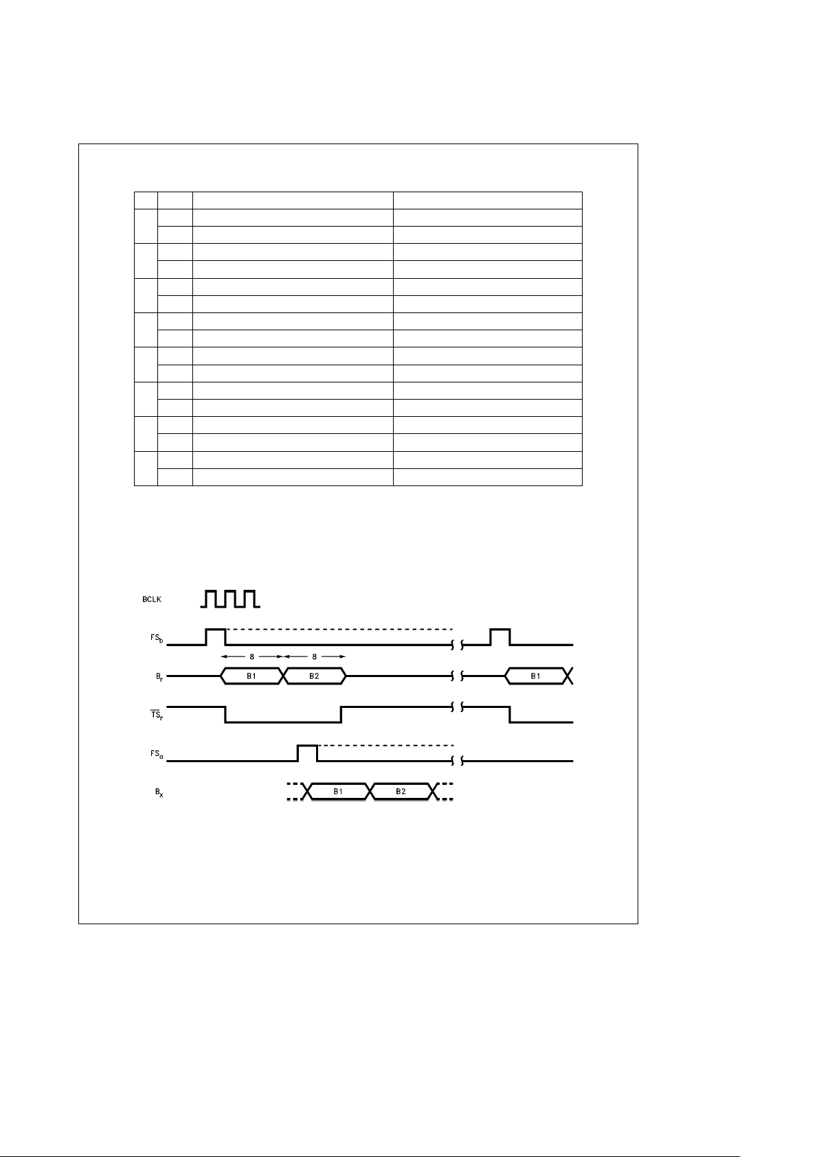
The digital system interface on the DASL separates B and D
channel information onto different pins to provide maximum
flexibility. On the B channel interface, phase skew between
transmit and receive directions may be accommodated at
the Master end since separate frame sync inputs, Fs
a
and
Fs
b
, are provided. Each of these synchronizes a counter
which gates the transfer of B1 and B2 channels in consecutive time-slots across the digital interface; since the counters are edge-synchronized the duration of the F
s
input signals may vary from a single-bit pulse to a square-wave. The
serial shift rate is determined by the BCLK input, and may
be any frequency from 256 kHz to 2.048 MHz, as shown in
Figure 6.
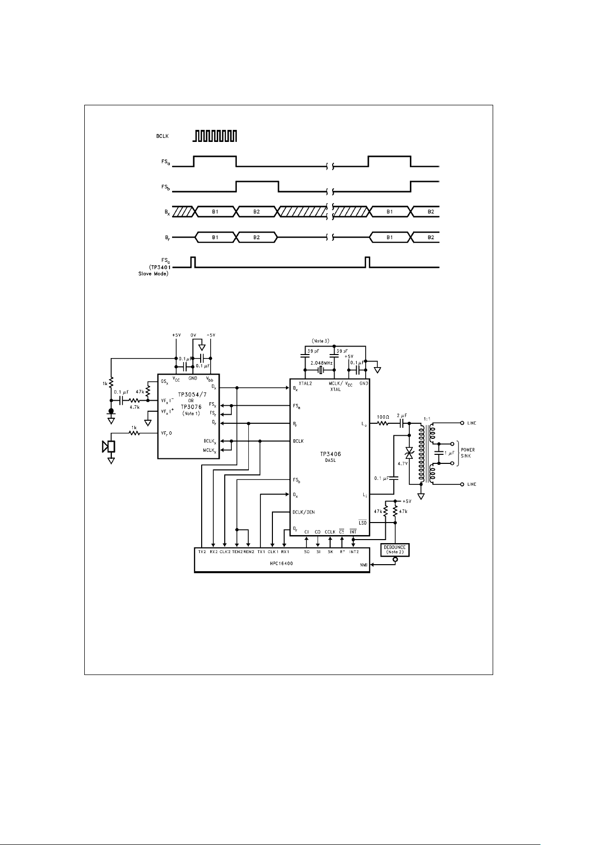
At the Slave end, both Fsaand Fsbare outputs. Fsagoes
high for 8 cycles of BCLK coincident with the 8 bits of the
B1 channel in both Transmit and Receive directions. Fs
b
goes high for the next 8 cycles of BCLK, which are coincident with the 8 bits of the B2 channel in both Transmit and
Receive directions. BCLK is also an output at 2.048 MHz,
the serial data shift rate, as shown in
Figure 7.
Data may be
exchanged between the B1 and B2 channels as it passes
through the device, by setting Control bit C0
e
1. An addi-
tional Frame Sync output, FS
c
, is provided to enable a regenerator to be built by connecting a DASL in Slave Mode
to a DASL in Master Mode. The FS
c
output from the Slave
directly drives the FS
a
and FSbinputs on the Master.
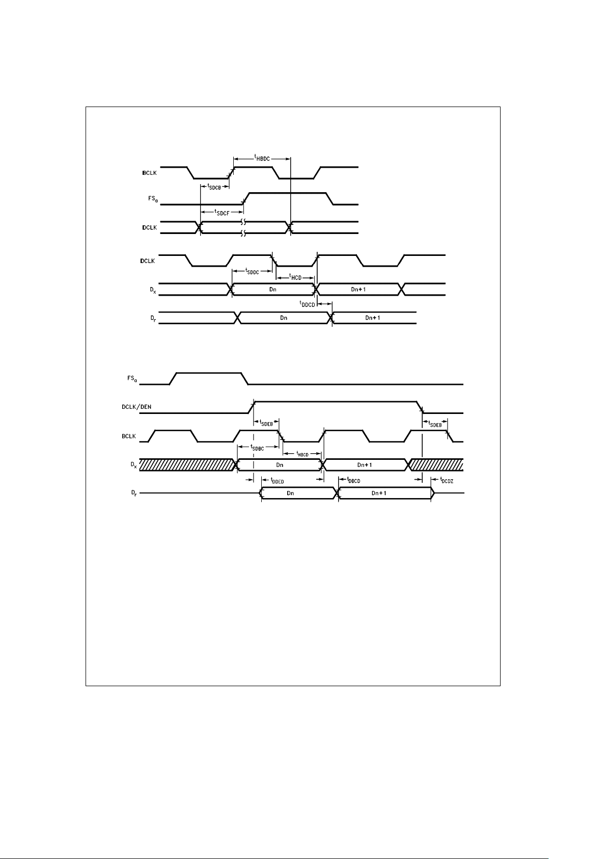
D channel information, being packet-mode, requires no synchronizing input. This interface consists of the transmit data
input, D
x
, receive data output, Dr, and 16 kHz serial shift
clock DCLK, which is an input at the Master end and an
output at the Slave end. Data shifts into D
x
on falling edges
of DCLK and out from D
r
on rising edges, as shown in
Fig-
ure 11.
DCLK should be Synchronous with BCLK.
An alternative function of the DCLK/DEN pin allows Dxand
D
r
to be clocked at the same rate as BCLK at the Master
end only. By setting bit C1 in the Control Register to a 1,
DCLK/DEN becomes an input for an enabling pulse to gate
2 cycles of BCLK for shifting the 2 D bits per frame. Thus, at
the Master end, the D channel bits can be interfaced to a
TDM bus and assigned to a time-slot (the same time-slot for
both transmit and receive), as shown in
Figure 12.
CONTROL INTERFACE
A serial interface, which can be clocked independently from
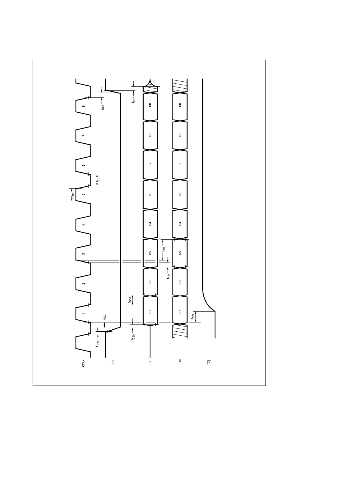
the B and D channel system interfaces, is provided for microprocessor control of various functions on the DASL device. All data transfers consist of a single byte shifted into
the Control Register via CI simultaneous with a single byte
shifted out from the Status Register via CO, see
Figure 13
.
Data shifts in to CI on rising edges of CCLK and out from
CO on falling edges when CS
is pulled low for 8 cycles of
CCLK. An Interrupt output, INT
goes low to alert the microprocessor whenever a change in one of the status bits, C1
and/or C0 has occurred. This latched output is cleared high
following the first CCLK pulse when CS
is low. No interrupt
is generated when status bit C2 (bipolar violation) goes high,
however. This bit is set whenever 1 or more violations of the
AMI coding rule is received, and cleared everytime the CS
is
pulsed. Statistics on the line bit error rate can be accumulated by regularly polling this bit.
When reading the CO pin, data is always clocked into the
Control Register; therefore the CI data word should repeat
the previous instruction if no change to the device mode is
intended.
Figure 13
shows the timing for this interface, and Table II
lists the control functions and status indicators.
5
Page 6
Functional Description (Continued)
TABLE II. Control and Status Register Functions
Bit State Control Register Function Status Register Function
C7
0 Master Mode Read Back C7 from Control Register
1 Slave Mode Read Back C7 from Control Register
C6
0 Deactivate and Power Down Read Back C6 from Control Register
1 Power Up and Activate Read Back C6 from Control Register
C5
0 Normal Through Connection Read Back C5 from Control Register
1 Loopback to Digital Interface Read Back C5 from Control Register
C4
0 Normal Through Connection Read Back C4 from Control Register
1 Loopback B1aB2aD to Line (Note 1) Read Back C4 from Control Register
C3
0 Normal Through Connection Read Back C3 from Control Register
1 Loopback B1 Only to Line (Note 1) Read Back C3 from Control Register
C2
0 Normal Through Connection No Error
1 Loopback B2 Only to Line (Note 1) Bipolar Violation Since Last READ (Note 2)
C1
0 DCLK/DEN pin
e
16 kHz Clock Out-Of-Sync
1 DCLK/DEN pineD Channel Enable (Note 3) Loop In-Sync and Activation Complete
C0
0 B1/B2 Channels Direct No Line Signal at Receiver Input
1 B1/B2 Channels Exchanged Line Signal Present at Receiver Input
Note 1: Receive data active.
Note 2: After the device is in sync.
Note 3: In Master mode only.
Note 4: C7 is the first bit clocked in and out of the device.
Timing Diagrams
TL/H/11725– 6
FIGURE 6. B Channel Interface Timing: Master Mode
6
Page 7
Timing Diagrams (Continued)
TL/H/11725– 7
FIGURE 7. B Channel Interface Timing: Slave Mode
Typical Applications
TL/H/11725– 8
FIGURE 8. Typical Application for Slave End
Note 1: The TP3076 Programmable Combos also must be connected to the MICROWIRE interface.
Note 2: Only necessary if a mechanical Hookswitch is connected to the NMI input of the HPC.
Note 3: Crystal load capacitors include board and trace capacitance. Oscillator frequency can be checked by measuring the BCLK output frequency when slave
mode part is in digital loopback.
7
Page 8
Typical Applications (Continued)
TL/H/11725– 9
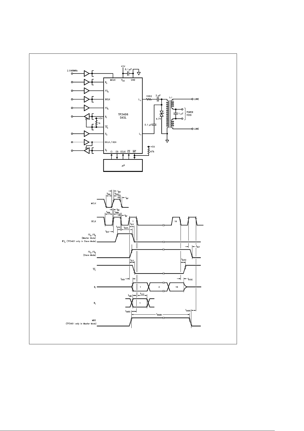
FIGURE 9. Typical Application for Master End
Timing Diagrams (Continued)
TL/H/11725– 10
FIGURE 10. B Channel Interface Timing Details
8
Page 9
Timing Diagrams (Continued)
TL/H/11725– 11
TL/H/11725– 12
FIGURE 11. D Channel Interface Timing (Master and Slave Modes, C1e0)
TL/H/11725– 13
FIGURE 12. D Channel Interface Timing (Master Mode only, C1e1)
9
Page 10
Timing Diagrams (Continued)
TL/H/11725– 14
FIGURE 13. Control Interface Timing
10
Page 11
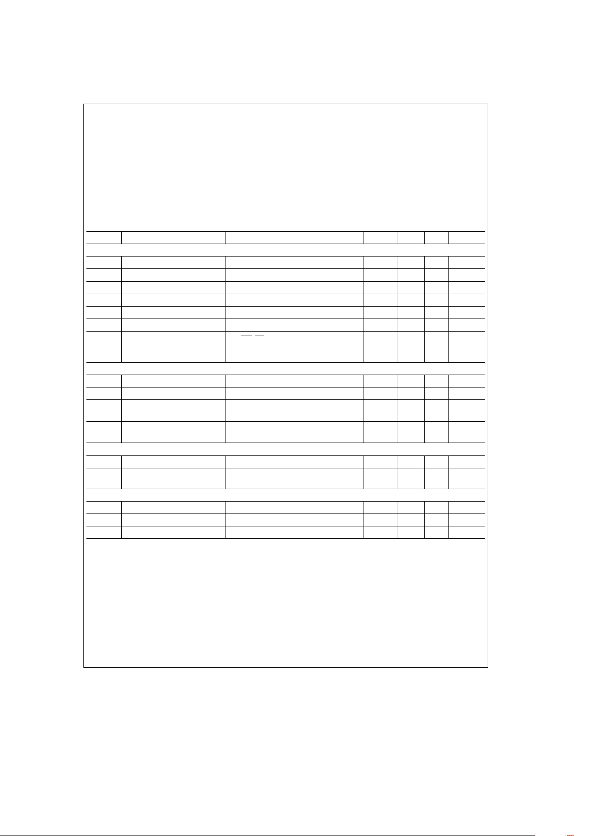
Absolute Maximum Ratings
If Military/Aerospace specified devices are required,
please contact the National Semiconductor Sales
Office/Distributors for availability and specifications.
V
CC
to GND 7V
Voltage at Li,L
o
V
CC
a
1V to V
SS
b
1V
Voltage at any Digital Input V
CC
a
1V to V
SS
b
1V
Storage Temperature Range
b
65§Ctoa150§C
Current at L
o
g
100 mA
Current at any Digital Output
g
50 mA
Lead Temperature (Soldering, 10 sec.) 300§C
ESD (Human Body Model) 2000V
Electrical Characteristics Unless otherwise noted, limits printed in bold characters are guaranteed for V
CC
e
5.0Vg5% and T
A
e
0§Ctoa70§C by correlation with 100% electrical testing at V
CC
e
5.0V and T
A
e
25§C. All other limits
are assured by correlation with other production tests and/or product design and characterization. Typical characteristics are
specified at V
CC
e
5.0V and T
A
e
25§C. All digital signals are referenced to GND.
Symbol Parameter Conditions Min Typ Max Units
DIGITAL INTERFACES
V
IL
Input Low Voltage All Digital Inputs (not MCLK) 0.7 V
V
IH
Input High Voltage All Digital Inputs (not MCLK) 2.2 V
V
OL
Output Low Voltage I
L
e
1 mA 0.4 V
V
OH
Output High Voltage I
L
eb
1 mA 2.4 V
I
IM
Input Current at MBS/FS
c
GNDkV
IN
k
V
CC
b
600 10 mA
I
I
Input Current Any Other Digital Input, GNDkV
IN
k
V
CC
b
10 10 mA
I
OZ
Output Current in Br, INT,TSr, CO, D
r
High Impedance GNDkV
OUT
k
V
CC
b
10 10 mA
State (TRI-STATE
É
)
LINE INTERFACES
R
Li
Input Resistance 0VkL
i
k
5.0V 50 kX
CL
Lo
Load Capacitance CLLofrom Loto GND. 100 pF
RO Output Resistance Loade60X in Series with 2 mFtoGND
3.0 X
at L
o
V
DC
Mean d.c. Voltage Loade60X in Series with 2 mFtoGND
2.0 V
at L
o
POWER DISSIPATION
ICC0 Power Down Current 1.3 2.5 mA
ICC1 Power Up Current (Activated) Load at L
o
e
200X in Series with 2 mFto
20 mA
GND (in Master Mode)
TRANSMISSION PERFORMANCE
Transmit Pulse Amplitude at LoR
L
e
200X in Series with 2 mFtoGND
g
1.1 Vpk
Input Pulse Amplitude at L
i
g
250 mVpk
Timing Recovery Jitter BCLK at Slave Relative to MCLK at Master 100 ns pk-pk
11
Page 12
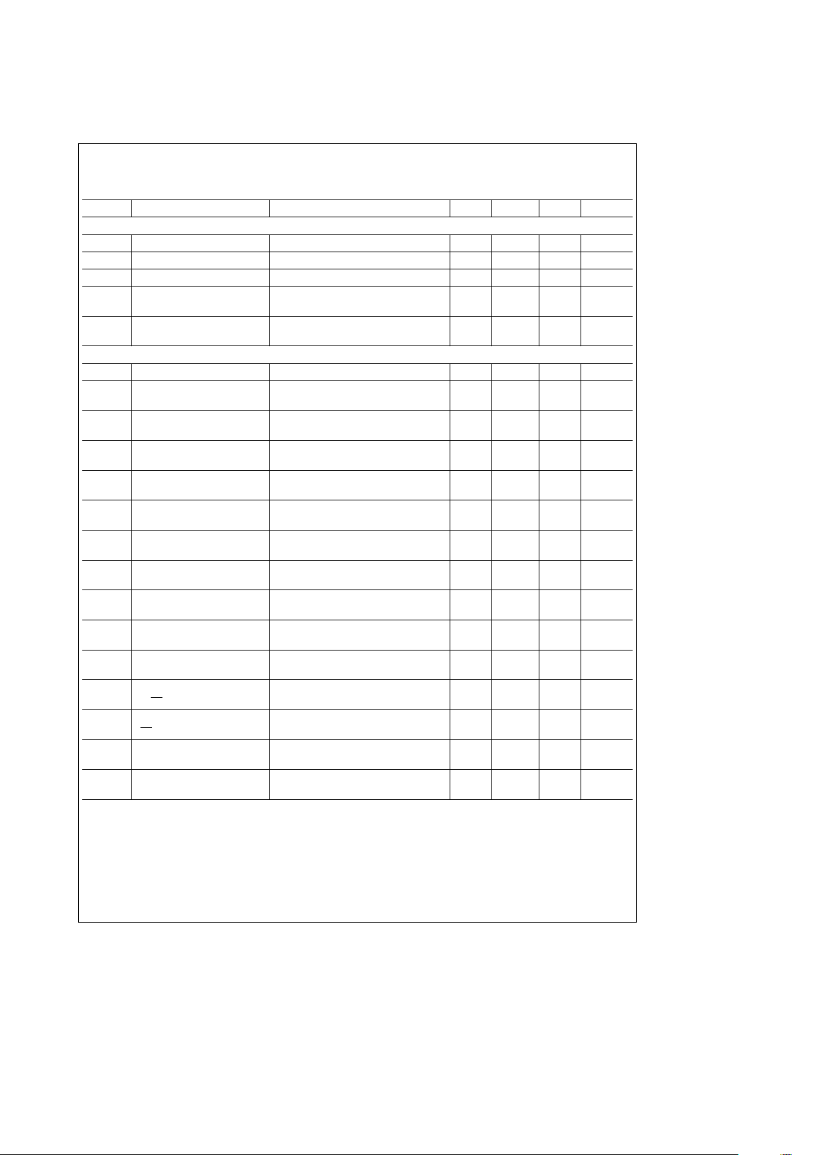
Timing Characteristics
Unless otherwise noted: V
CC
ea
5Vg5%, T
A
e
0§Cto70§C. Typical characteristics are specified at V
CC
e
5V, T
A
e
25§C.
All signals are referenced to GND.
Symbol Parameter Conditions Min Typ Max Units
MASTER CLOCK INPUT SPECIFICATIONS
F
MCK
Master Clock Frequency 2.048 MHz
Master Clock Tolerance Measured Relative to the Slave MCLK
b
100
a
100 ppm
Master Clock Input Jitter 2.048 MHz Input, 18 kHzkfk200 kHz 200 ns pk-pk
t
WMH,
Clock Pulse Width V
IH
e
V
CC
b
0.5V
190 ns
t
WML
Hi & Low for MCLK V
IL
e
0.5V
tMR, Rise and Fall Time Used as a Logic Input
15 ns
t
MF
of MCLK
B CHANNEL INTERFACE
(Figure 10)
F
BCK
Bit Clock Frequency Master Mode Only 2.048 MHz
t
WBH
, Clock Pulse Width V
IH
e
2.2V
190 ns
t
WBL
Hi & Low for BCLK V
IL
e
0.7V
tBR, Rise and Fall Time Master Mode requirement for BCLK
15 ns
Source
t
BF
of BCLK
t
SFB
Set-Up Time, FSaand Master Mode Only
70 ns
FSbto BCLK Low
t
HCFL
Hold Time, BCLK Low to Master Mode Only
100 ns
FS
a
and FSbLow
t
WBH
Output Pulse Width Slave Mode Only
195 ns
t
WBL
High and Low for BCLK Loade2 LSTTL Inputs Plus 50 pF
t
DCF
Delay Time, BCLK High to Slave Mode Only
115 ns
FSa,FSband FScTransitions Loade2 LSTTL Inputs Plus 50 pF
t
SBC
Set Up Time, BXValid
30 ns
to BCLK Low
t
HCB
Hold Time, BCLK Low to
50 ns
B
X
Invalid
t
DCB
Delay Time, BCLK High Loade2 LSTTL Inputs Plus 100 pF
160 ns
to B
r
Valid
t
DCBZ
Delay Time, BCLK Low to Slave Mode Only
60 220 ns
B
r
High-Impedance
t
DCT
Delay Time, BCLK High Loade2 LSTTL Inputs Plus 100 pF
180 ns
to TS
r
Low
t
DCTZ
Delay Time, BCLK Low to
60 185 ns
TS
r
High-Impedance
t
SMBC
Set-Up Time, MBS Master Mode Only
60 ns
to BCLK Low (Note 1)
t
WMBH
Width of MBS Input Master Mode Only
125 ms
High
Note 1: MBS transitions may occur anywhere in the Frame, and require no specific relationship to FSaor FSb.
12
Page 13
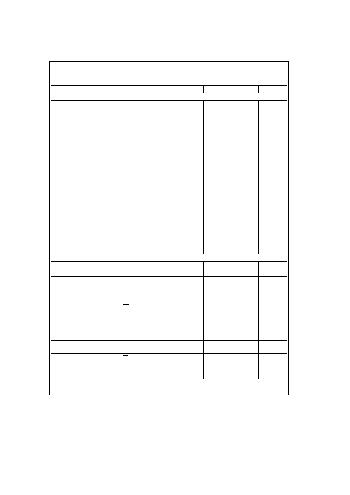
Timing Characteristics (Continued)
Unless otherwise noted: V
CC
ea
5Vg5%, T
A
e
0§Cto70§C. Typical characteristics are specified at V
CC
e
5V, T
A
e
25§C.
All signals are referenced to GND.
Symbol Parameter Conditions Min Max Units
D CHANNEL INTERFACE
(Figure 11&12)
t
SDDC
Set Up Time, D
X
100 ns
Valid to DCLK Low
t
HCD
Hold Time, DCLK Low
100 ns
to D
X
Invalid
t
DDCD
Delay Time, DCLK High to Loade100 pF
220 ns
D
r
Data Valid
a
2 LSTTL Inputs
t
SDCB
Set-Up Time, DCLK Master Mode
50 ns
Transitions to BCLK High Only
t
HBDC
Hold Time, BCLK High Master Mode
50 ns
to DCLK Transitions Only
t
SDCF
Set-Up Time, DCLK Master Mode
70 ns
Transitions to FS
a
HIgh Only
t
DDED
Delay Time, DEN High Loade100 pF
a
200 ns
to D
r
Valid 2 LSTTL Inputs
t
SDEB
Set-Up Time, DEN to
100 ns
BCLK Low
t
SDBC
Set-Up Time, D
x
50 ns
to BCLK Low
t
HBCD
Hold Time, BCLK
50 ns
Low to DxInvalid
t
DBCD
Delay Time, BCLK Loade100 pF
190 ns
High to D
r
Valid
a
2 LSSTL Inputs
t
DCDZ
Delay Time, DEN
140 ns
Low to D
r
High Impedance
CONTROL INTERFACE
(Figure 13)
t
CH
CCLK High Duration 250 ns
t
CL
CCLK Low Duration 250 ns
t
SIC
Setup Time, CI
100 ns
Valid to CCLK High
t
HCI
Hold Time, CCLK High
0 ns
to CI Invalid
t
SSC
Setup Time from CS
200 ns
Low to CCLK High
t
HCS
Hold Time from CCLK
10 ns
Low to CS
t
DCO
Delay Time from CCLK Low Loade100 pF
150 ns
to C0 Data Valid
a
2 LSTTL Inputs
t
DSO
Delay Time from CS 1st Bit Only
100 ns
Low to CO Valid
t
DSZ
Delay Time from CS High
100 ns
to CO High Impedance
t
DCI
Delay Time from CCLK1
120 ns
High to INT
High Impedance
13
Page 14

Definitions and Timing Conventions
DEFINITIONS
V
IH
VIHis the d.c. input level above which
an input level is guaranteed to appear
as a logical one. This parameter is to
be measured by performing a functional test at reduced clock speeds and
nominal timing, (i.e. not minimum setup
and hold times or output strobes), with
the high level of all driving signals set
to V
IH
and maximum supply voltages
applied to the device.
V
IL
VILis the d.c. input level below which
an input level is guaranteed to appear
as a logical zero to the device. This parameter is measured in the same manner as V
IH
but with all driving signal low
levels set to V
IL
and minimum supply
voltages applied to the device.
V
OH
VOHis the minimum d.c. output level to
which an output placed in a logical one
state will converge when loaded at the
maximum specified load current.
V
OL
VOLis the maximum d.c. output level to
which an output placed in a logical zero
state will converge when loaded at the
maximum specified load current.
Threshold Region The threshold region is the range of in-
put voltages between V
IL
and VIH.
Valid Signal A signal is Valid if it is in one of the
valid logic states, (i.e. above V
IH
or be-
low V
IL
). In timing specifications, a signal is deemed valid at the instant it enters a valid state.
Invalid Signal A signal is Invalid if it is not in a valid
logic state, i.e. when it is in the threshold region between V
IL
and VIH. In timing specifications, a signal is deemed
invalid at the instant it enters the
threshold region.
TIMING CONVENTIONS
For the purpose of this timing specification the following
conventions apply:
Input Signals All input signals may be characterized
as: V
L
e
0.4V, V
IH
e
2.4V, t
R
k
10 ns,
t
F
k
10 ns.
Period The period of clock signal is designat-
ed at t
Pxx
where xx represents the
mnemonic of the clock signal being
specified.
Rise Time Rise times are designated at t
Ryy
,
where yy represents a mnemonic of
the signal whose rise time is being
specified. t
Ryy
is measured from VILto
V
IH
.
Fall Time Fall times are designated as t
Fyy
,
where yy represents a mnemonic of
the signal whose fall time is being
specified. t
Fyy
is measured from VIHto
V
IL
.
Pulse Width High The high width is designated as t
WzzH
,
where zz represents the mnemonic of
the input or output signal whose pulse
width is being specified. High pulse
widths are measured from V
IH
to VIH.
Pulse Width Low The low pulse width is designed as
t
WzzL
, where zz represents the mnemonic of the input or output signal
whose pulse width is being specified.
Low pulse widths are measured from
V
IL
to VIL.
Setup Time Setup times are designated as t
Swwxx
,
where ww represents the mnemonic of
the input signal whose setup time is being specified relative to a clock or
strobe input represented by mnemonic
xx. Setup times are measured from the
ww Valid to xx Invalid.
Hold Time Hold times are designated as t
Hxxww
,
where ww represents the mnemonic of
the input signal whose hold time is being specified relative to a clock or
strobe input represented by mnemonic
xx. Hold times are measured from xx
Valid to ww invalid.
Delay Time Delay times are designated as t
Dxxyy
[
lHl
L], where xx represents the mnemonic of the input reference signal and
yy represents the mnemonic of the output signal whose timing is being specified relative to xx. The mnemonic may
optionally be terminated by an H or L to
specifiy the high going or low going
transition of the output signal. Maximum delay times are measured from xx
Valid to yy Valid. Minimum delay times
are measured from xx Valid to yy invalid. This parameter is tested under the
load conditions specified in the Conditions column of the Timing Specification section of this data sheet.
14
Page 15

15
Page 16
TP3406 DASL Digital Adapter for Subscriber Loops
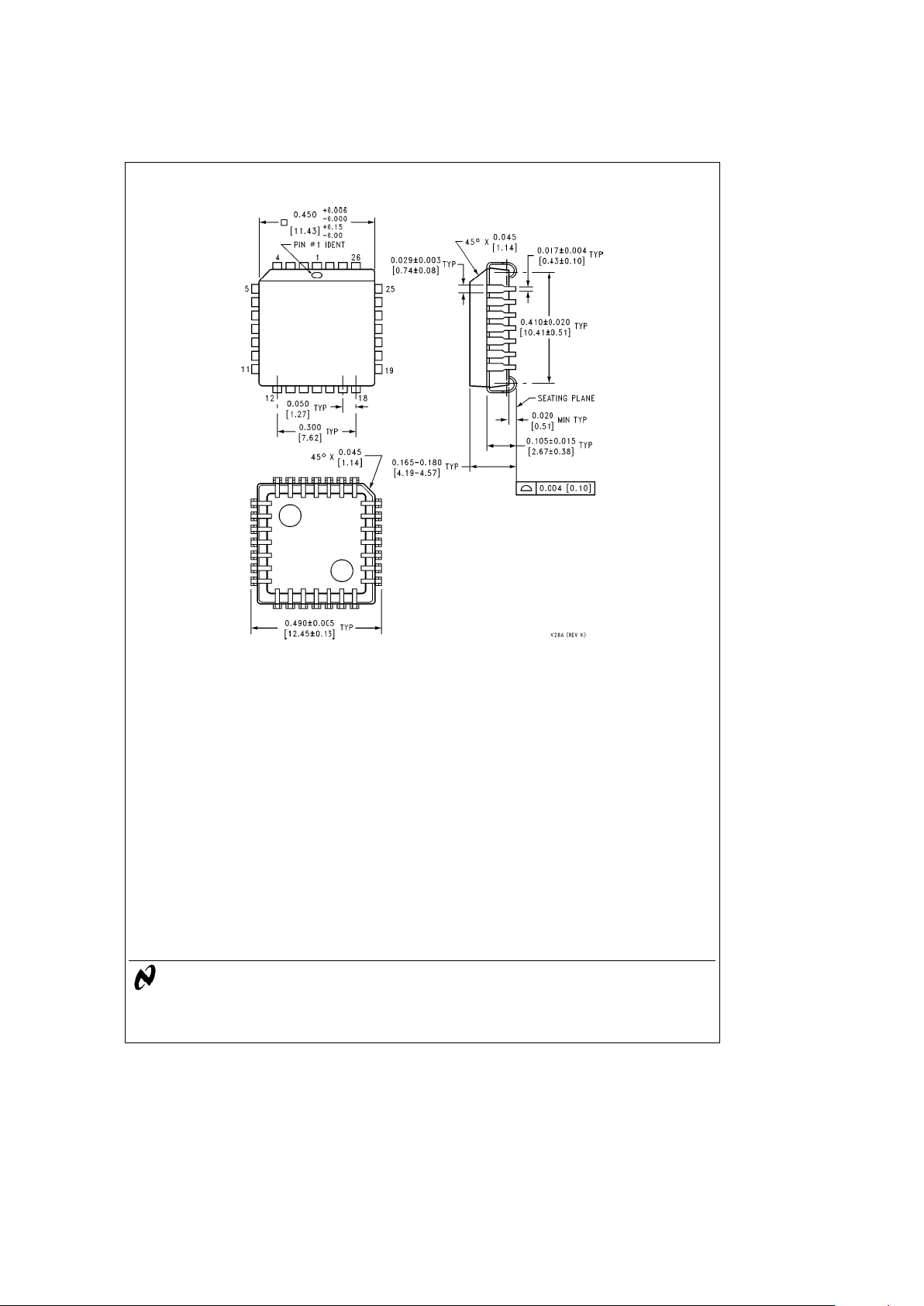
Physical Dimensions inches (millimeters)
Plastic Chip Carrier (V)
Order Number TP3406V
NS Package Number V28A
LIFE SUPPORT POLICY
NATIONAL’S PRODUCTS ARE NOT AUTHORIZED FOR USE AS CRITICAL COMPONENTS IN LIFE SUPPORT
DEVICES OR SYSTEMS WITHOUT THE EXPRESS WRITTEN APPROVAL OF THE PRESIDENT OF NATIONAL
SEMICONDUCTOR CORPORATION. As used herein:
1. Life support devices or systems are devices or 2. A critical component is any component of a life
systems which, (a) are intended for surgical implant support device or system whose failure to perform can
into the body, or (b) support or sustain life, and whose be reasonably expected to cause the failure of the life
failure to perform, when properly used in accordance support device or system, or to affect its safety or
with instructions for use provided in the labeling, can effectiveness.
be reasonably expected to result in a significant injury
to the user.
National Semiconductor National Semiconductor National Semiconductor National Semiconductor
Corporation Europe Hong Kong Ltd. Japan Ltd.
1111 West Bardin Road Fax: (
a
49) 0-180-530 85 86 13th Floor, Straight Block, Tel: 81-043-299-2309
Arlington, TX 76017 Email: [email protected] Ocean Centre, 5 Canton Rd. Fax: 81-043-299-2408
Tel: 1(800) 272-9959 Deutsch Tel: (
a
49) 0-180-530 85 85 Tsimshatsui, Kowloon
Fax: 1(800) 737-7018 English Tel: (
a
49) 0-180-532 78 32 Hong Kong
Fran3ais Tel: (
a
49) 0-180-532 93 58 Tel: (852) 2737-1600
Italiano Tel: (
a
49) 0-180-534 16 80 Fax: (852) 2736-9960
National does not assume any responsibility for use of any circuitry described, no circuit patent licenses are implied and National reserves the right at any time without notice to change said circuitry and specifications.
 Loading...