

Page 1
TP5089 DTMF (TOUCH-TONE) Generator
TP5089 DTMF(TOUCH-TONE) Generator
December 1991
General Description
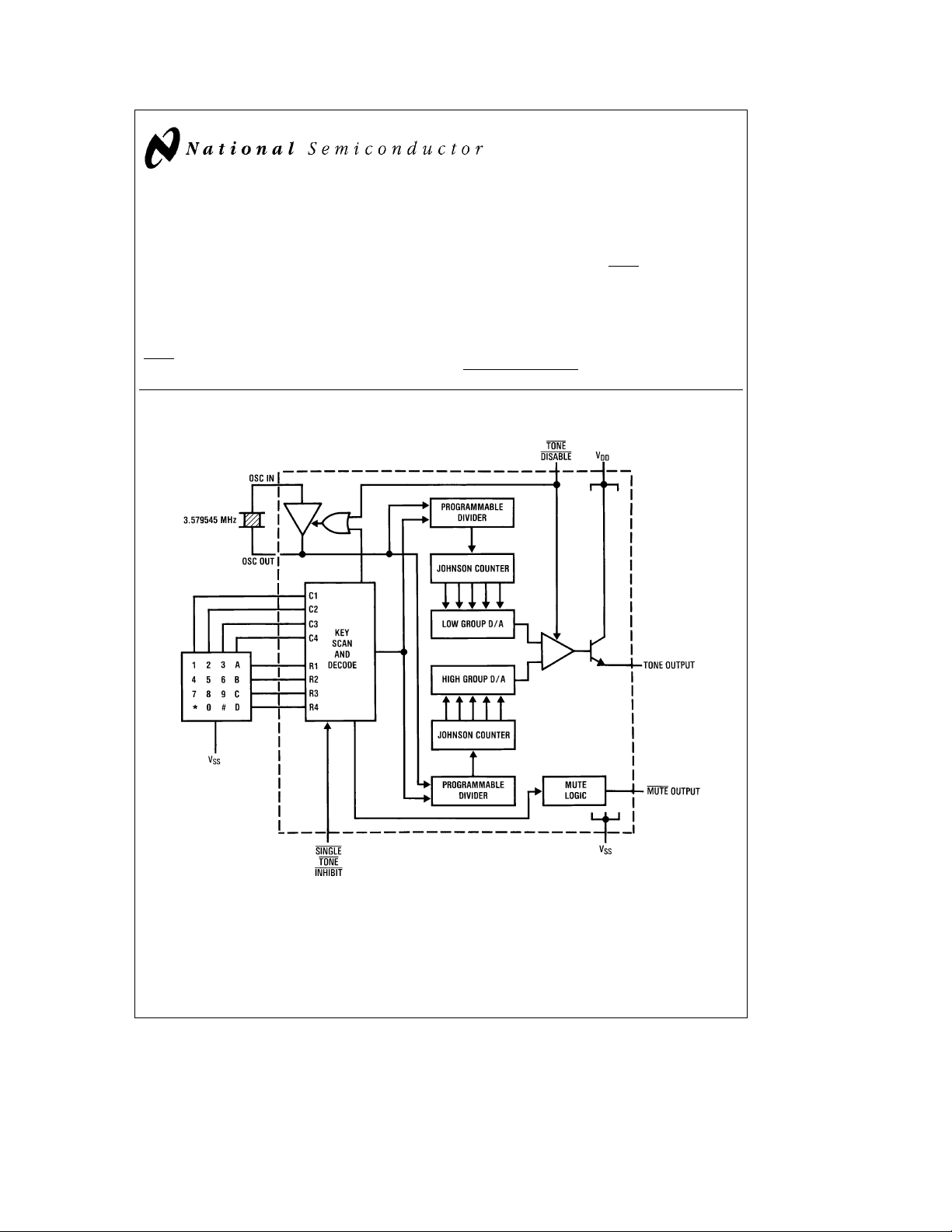
The TP5089 is a low threshold voltage, field-implanted, metal gate CMOS integrated circuit. It interfaces directly to a
standard telephone keypad and generates all dual tone multi-frequency pairs required in tone-dialing systems. The tone
synthesizers are locked to an on-chip reference oscillator
using an inexpensive 3.579545 MHz crystal for high tone
accuracy. The crystal and an output load resistor are the
only external components required for tone generation. A
MUTE
OUT logic signal, which changes state when any key
is depressed, is also provided.
Block Diagram
Features
Y
3.5V–10V operation when generating tones
Y
2V operation of keyscan and MUTE logic
Y
Static sensing of key closures or logic inputs
Y
On-chip 3.579545 MHz crystal-controlled oscillator
Y
Output amplitudes proportional to supply voltage
Y
High group pre-emphasis
Y
Low harmonic distortion
Y
Open emitter-follower low-impedance output
Y
SINGLE TONE INHIBIT pin
FIGURE 1
TL/H/5057– 1
C
1995 National Semiconductor Corporation RRD-B30M115/Printed in U. S. A.
TL/H/5057
Page 2
Absolute Maximum Ratings
If Military/Aerospace specified devices are required,
please contact the National Semiconductor Sales
Office/Distributors for availability and specifications.
Supply Voltage (V
Maximum Voltage at Any Pin V
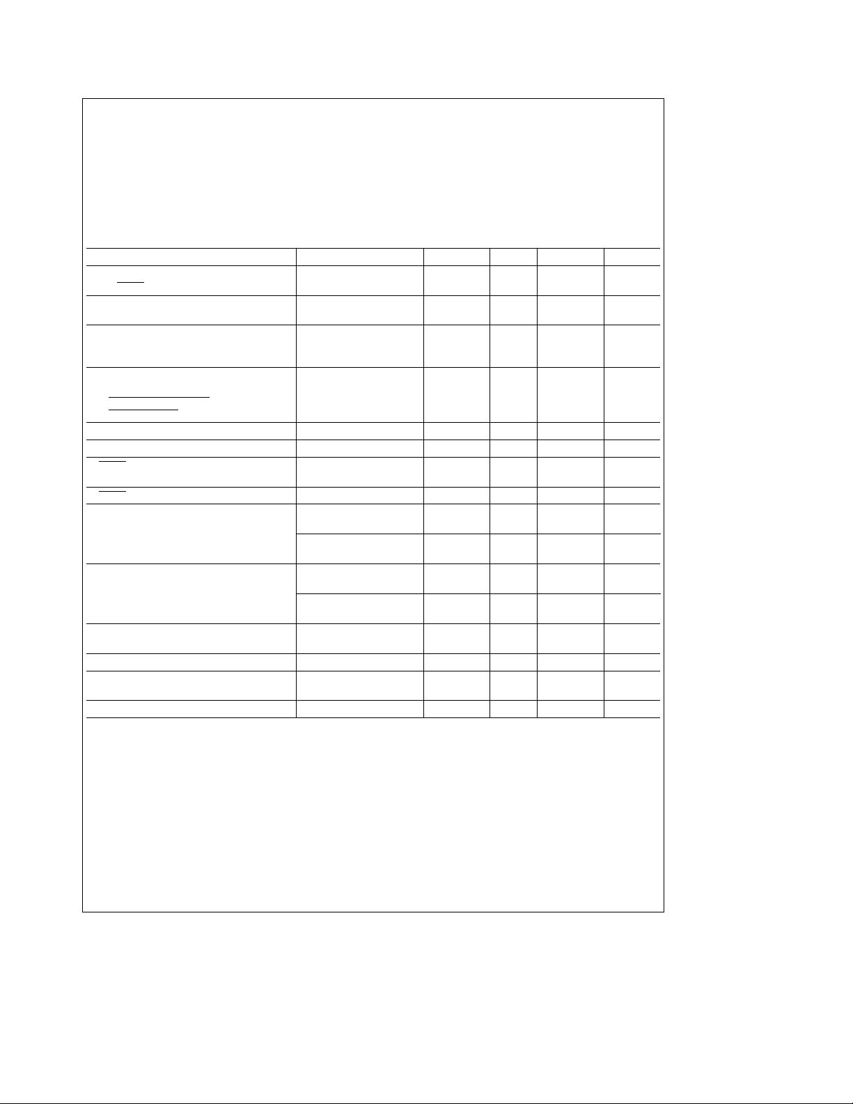
Electrical Characteristics Unless otherwise noted, limits printed in BOLD characters are guaranteed for V
3.5V to 10V, T
correlation with other production tests and/or product design and characterization.
b
VSS) 15V
DD
e
0§Ctoa60§C by correlation with 100% electrical testing at T
A
DD
a
0.3V to V
b
0.3V
SS
Operating Temperature
Storage Temperature
Maximum Power Dissipation 500 mW
e
25§C. All other limits are assured by
A
Parameter Conditions Min Typ Max Units
Minimum Supply Voltage for Keysense
and MUTE
Logic Functions
Minimum Operating Voltage
for generating tones
Operating Current Mute open
Idle R
Generating Tones V
L
DD
e %
e
3.5V
2V
3.5 V
2 25 mA
1.1 2.5 mA
Input Resistors
COLUMN and ROW (Pull-Up) 25 50 kX
SINGLE TONE INHIBIT
TONE DISABLE
(Pull-Down) 120 kX
(Pull-Up)
Input Low Level 0.2 V
Input High Level 0.8 V
MUTE OUT Sink Current V
(COLUMN and ROW Active) V
MUTE Out Leakage Current V
Output Amplitude R
Low Group V
Output Amplitude R
High Group V
Mean Output DC Offset V
e
3.5V
DD
e
0.5V
o
e
V
o
DD
e
240 X
L
e
3.5V
DD
e
R
240X
L
e
10V
V
DD
e
240X
L
e
3.5V
DD
e
R
240X
L
e
10V
V
DD
e
3.5V 1.3 V
DD
e
V
10V 4.6 V
DD
DD
0.4 mA
1 mA
190 250 340 mVrms
510 700 880 mVrms
270 340 470 mVrms
735 955 1265 mVrms
High Group Pre-Emphasis 2.2 2.7 3.2 dB
Dual Tone/Total Harmonic Distortion Ratio V
e
DD
1 MHz Bandwidth
4V, R
e
240X
L
b
23
Start-Up Time (to 90% Amplitude) 3 5 mS
Note 1: RLis the external load resistor connected from TONE OUT to VSS.
Note 2: Crystal specification: Parallel resonant 3.579545 MHz, R
s
150 X,Le100 mH, C
S
e
e
5 pF, C
O
I
0.02 pF.
b
30§Ctoa60§C
b
55§Ctoa150§C
DD
b
22 dB
DD
e
V
V
2
Page 3
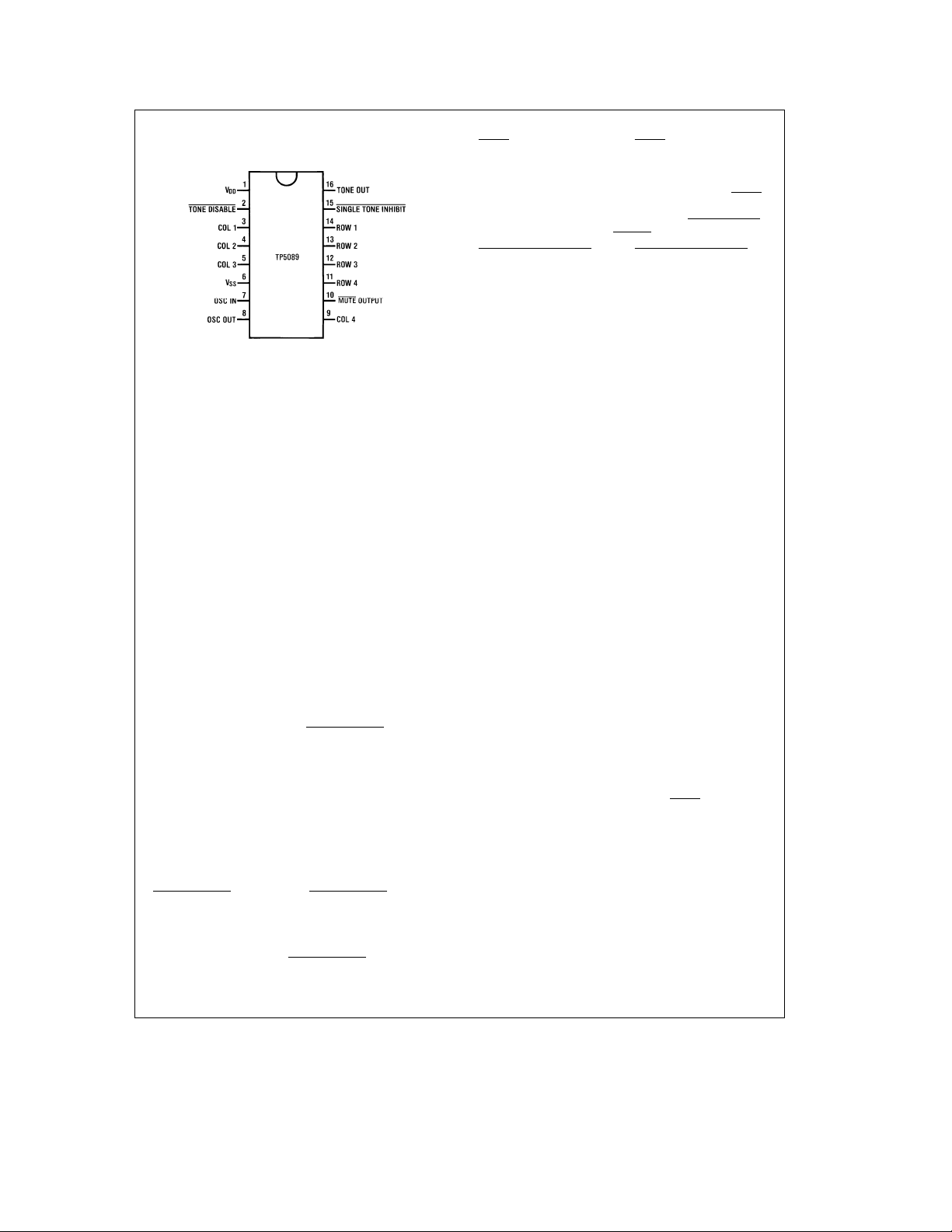
Connection Diagram
Dual-In-Line Package
Top View
TL/H/5057– 2
Order Number TP5089N
See NS Package N16A
Pin Descriptions
Symbol Description
V
DD
V
SS
OSC IN, OSC OUT All tone generation timing is
Row and Column Inputs When no key is pushed, pull-up
TONE DISABLE
Input an internal pull-up resistor.
This is the positive voltage
supply to the device, referenced
to V
. The collector of the
SS
TONE OUT transistor is
connected to this pin.
This is the negative voltage
supply. All voltages are
referenced to this pin.
derived from the on-chip
oscillator circuit. A low cost
3.579545 MHz A-cut crystal
(NTSC TV color-burst) is
needed between pins 7 and 8.
Load capacitors and a feedback
resistor are included on-chip for
good start-up and stability. The
oscillator stops when column
inputs are sensed with no valid
input having been detected. The
oscillator is also stopped when
the TONE DISABLE
input is
pulled to logic low.
resistors are active on row and
column inputs. A key closure is
recognized when a single row
and a single column are
connected to V
the oscillator and initiates tone
, which starts
SS
generation. Negative-true logic
signals simulating key closures
can also be used.
The TONE DISABLE input has
When this input is open or at
logic high, the normal tone
output mode will occur. When
TONE DISABLE
input is at logic
low, the device will be in the
inactive mode, TONE OUT will
be at an open circuit state.
Symbol Description
MUTE
Output The MUTE output is an open-
drain N-channel device that
sinks current to V
key input and is open when no
SS
with any
key input is sensed. The MUTE
output will switch regardless of
the state of the SINGLE TONE
INHIBIT input.
SINGLE TONE INHIBIT The SINGLE TONE INHIBIT
Input input is used to inhibit the
generation of other than valid
tone pairs due to multiple rowcolumn closures. It has a pulldown resistor to V
left open or tied to V
input condition that would
, and when
SS
any
SS
normally result in a single tone
will now result in no tone, with
all other functions operating
normally. When tied to V
single or dual tones may be
DD
,
generated, see Table II.
TONE OUT This output is the open emitter
of an NPN transistor, the
collector of which is connected
to V
. When an external load
DD
resistor is connected from
TONE OUT to V
voltage on this pin is the sum of
, the output
SS
the high and low group sinewaves superimposed on a DC
offset. When not generating
tones, this output transistor is
turned OFF to minimize the
device idle current.
Adjustment of the emitter load
resistor results in variation of
the mean DC current during
tone generation, the sinewave
signal current through the
output transistor, and the output
distortion. Increasing values of
load resistance decrease both
the signal current and distortion.
Functional Description
With no key inputs to the device the oscillator is inhibited,
the output transistor is pulled OFF and device current consumption is reduced to a minimum. Key closures are sensed
statically. Any key closure activates the MUTE
the oscillator and sets the high group and low group programmable counters to the appropriate divide ratio. These
counters sequence two ratioed-capacitor D/A converters
through a series of 28 equal duration steps per sine-wave
cycle. The two tones are summed by a mixer amplifier, with
pre-emphasis applied to the high group tone. The output is
an NPN emitter-follower requiring the addition of an external
load resistor to V
the signal current flowing from V
sistor.
. This resistor facilitates adjustment of
SS
through the output tran-
DD
The amplitude of the output tones is directly proportional to
the device supply voltage.
output, starts
3
Page 4
Functional Description (Continued)
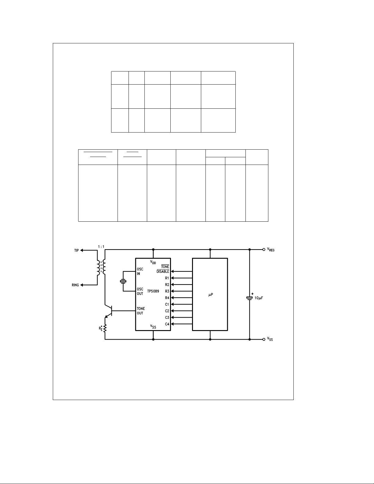
TABLE I. Output Frequency Accuracy
Tone Valid Standard Tone Output % Deviation
Group Input DTMF (Hz) Frequency from Standard
Low R1 697 694.8
Group R2 770 770.1
Group C2 1336 1331.7
SINGLE TONE TONE
INHIBIT DISABLE
X O O/C O/C 0V 0V O/C
X X O/C O/C 0V 0V O/C
X 0 One One V
X 1 One One f
1 1 2 or More One Ð f
1 1 One 2 or More f
1 1 2 or More 2 or More V
0 1 2 or More One V
0 1 One 2 or More V
0 1 2 or More 2 or More V
Note 1: X is don’t care state.
Note 2: V
is the output offset voltage.
OS
R3 852 852.4
f
L
R4 941 940.0
High C1 1209 1206.0
C3 1477 1486.5
f
H
C4 1633 1639.0
TABLE II. Functional Truth Table
ROW COLUMN
b
0.32
a
0.02
a
0.03
b
0.11
b
0.24
b
0.32
a
0.64
a
0.37
TONE OUT
Low High
V
OS
L
L
OS
OS
OS
OS
OS
f
H
H
ÐO
V
OS
V
OS
V
OS
V
OS
MUTE
O
O
O
O
O
O
O
*Adjust REfor desired tone amplitude.
FIGURE 2. Typical Application
4
TL/H/5057– 3
Page 5

5
Page 6
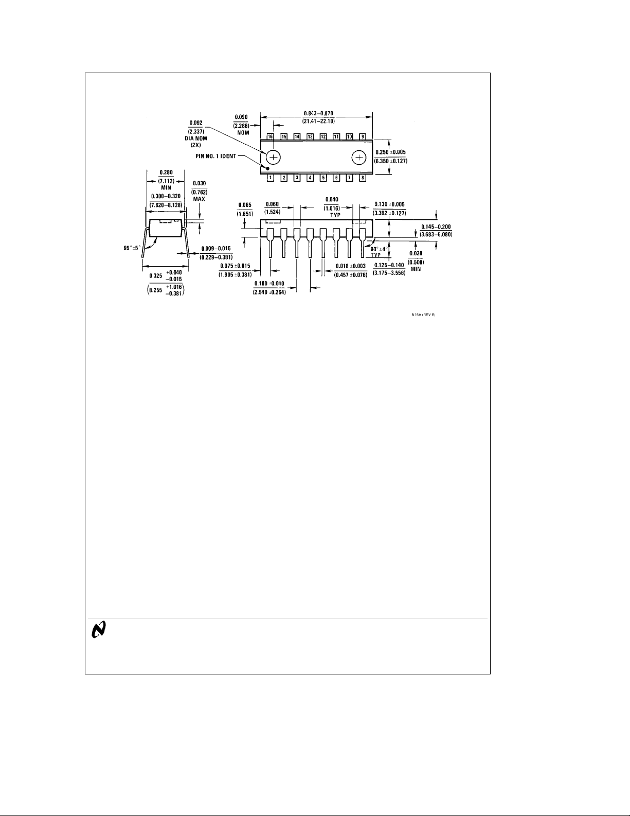
Physical Dimensions inches (millimeters) Lit.
Ý
113986
TP5089 DTMF(TOUCH-TONE) Generator
Molded Dual-In-Line Package (N)
Order Number TP5089N
NS Package N16A
LIFE SUPPORT POLICY
NATIONAL’S PRODUCTS ARE NOT AUTHORIZED FOR USE AS CRITICAL COMPONENTS IN LIFE SUPPORT
DEVICES OR SYSTEMS WITHOUT THE EXPRESS WRITTEN APPROVAL OF THE PRESIDENT OF NATIONAL
SEMICONDUCTOR CORPORATION. As used herein:
1. Life support devices or systems are devices or 2. A critical component is any component of a life
systems which, (a) are intended for surgical implant support device or system whose failure to perform can
into the body, or (b) support or sustain life, and whose be reasonably expected to cause the failure of the life
failure to perform, when properly used in accordance support device or system, or to affect its safety or
with instructions for use provided in the labeling, can effectiveness.
be reasonably expected to result in a significant injury
to the user.
National Semiconductor National Semiconductor National Semiconductor National Semiconductor
Corporation Europe Hong Kong Ltd. Japan Ltd.
1111 West Bardin Road Fax: (
Arlington, TX 76017 Email: [email protected] Ocean Centre, 5 Canton Rd. Fax: 81-043-299-2408
Tel: 1(800) 272-9959 Deutsch Tel: (
Fax: 1(800) 737-7018 English Tel: (
National does not assume any responsibility for use of any circuitry described, no circuit patent licenses are implied and National reserves the right at any time without notice to change said circuitry and specifications.
Fran3ais Tel: (
Italiano Tel: (
a
49) 0-180-530 85 86 13th Floor, Straight Block, Tel: 81-043-299-2309
a
49) 0-180-530 85 85 Tsimshatsui, Kowloon
a
49) 0-180-532 78 32 Hong Kong
a
49) 0-180-532 93 58 Tel: (852) 2737-1600
a
49) 0-180-534 16 80 Fax: (852) 2736-9960
 Loading...