

Page 1
现货库存、技术资料、百科信息、热点资讯,精彩尽在鼎好!
Data Sheet TLE6284G
H-Bridge Driver IC
Features
•
Compatible to very low ohmic normal
level input N-Channel MOSFETs
•
PWM – DIR - Interface
•
PWM frequency up to 50kHz
•
Operates down to 7.5 V
supply voltage
•
Low EMC sensitivity and emission
•
Adjustable dead time with shoot through protection
• Deactivation of dead time and shoot through protection possible
•
Short circuit protection for each Mosfet can be disabled and adjusted
•
Driver undervoltage shut down
•
Reverse polarity protection for the driver IC
•
Fast disable function / Inhibit for low quiescent current
•
Input with TTL characteristics
•
2 bit diagnosis
•
Thermal overload warning for driver IC
•
Shoot through protection
•
Integrated bootstrap diodes
Product Summary
Turn on current I
Turn off current I
Supply voltage range V
Gxx(on)
Gxx(off)
Vs
850 mA
580 mA
7.5 … 60 V
Gate Voltage VGS 10 V
Temperature range T
J
-40...+150 °C
P-DSO-20
Application
•
Dedicated for DC-brush high current motor bridges in PWM control mode for 12, 24 and 42V powernet applica-
tions.
•
The input structure allows an easy control of a DC-brush motor
General Description
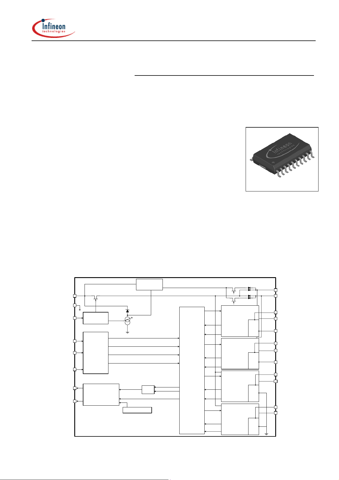
H-bridge driver IC for MOSFET power stages with multiple protection functions.
The TLE6184G is very similar to the TLE6281G. The major difference is that the Short Circuit protection level of
the TLE6284G can be adjusted by external resistors or even disabled. The pin outs are different as well.
Block Diagram
Charge Pump
OR
Short Cir cuit Detection
Tj > 170oC typ.
Undervoltage HSx
Undervoltage LSx
Level
Shift
Floating HS Dr iver 1
+
limitation HS1
V
GS
+
Short circu it
detect.
+
Undervoltage
Floating HS Dr iver 2
+
V
limitation HS2
GS
+
Short circu it
detect.
+
Undervoltage
Floating LS Dri ver 1
+
V
limitation LS1
GS
+
Short circu it
detect.
+
Undervoltage
Floating LS Dri ver 2
+
V
limitation LS2
GS
+
Short circu it
detect.
+
Undervoltage
BH1
BH2
DH1
GH1
SCD
SH1
DH2
GH2
SCD
SH2
DL1
GL1
SCD
DL2
GL2
SCD
V
S
GND
INH
PWM
DIR
DT/DIS
ER1
ER2
Linear
Regulator
INH
HS1
Input control
Dead time
Undervoltage
Short circuit Detect.
Overtemp. warning
LS1
HS2
LS2
1 2006-01-30
Page 2
Data Sheet TLE6284G
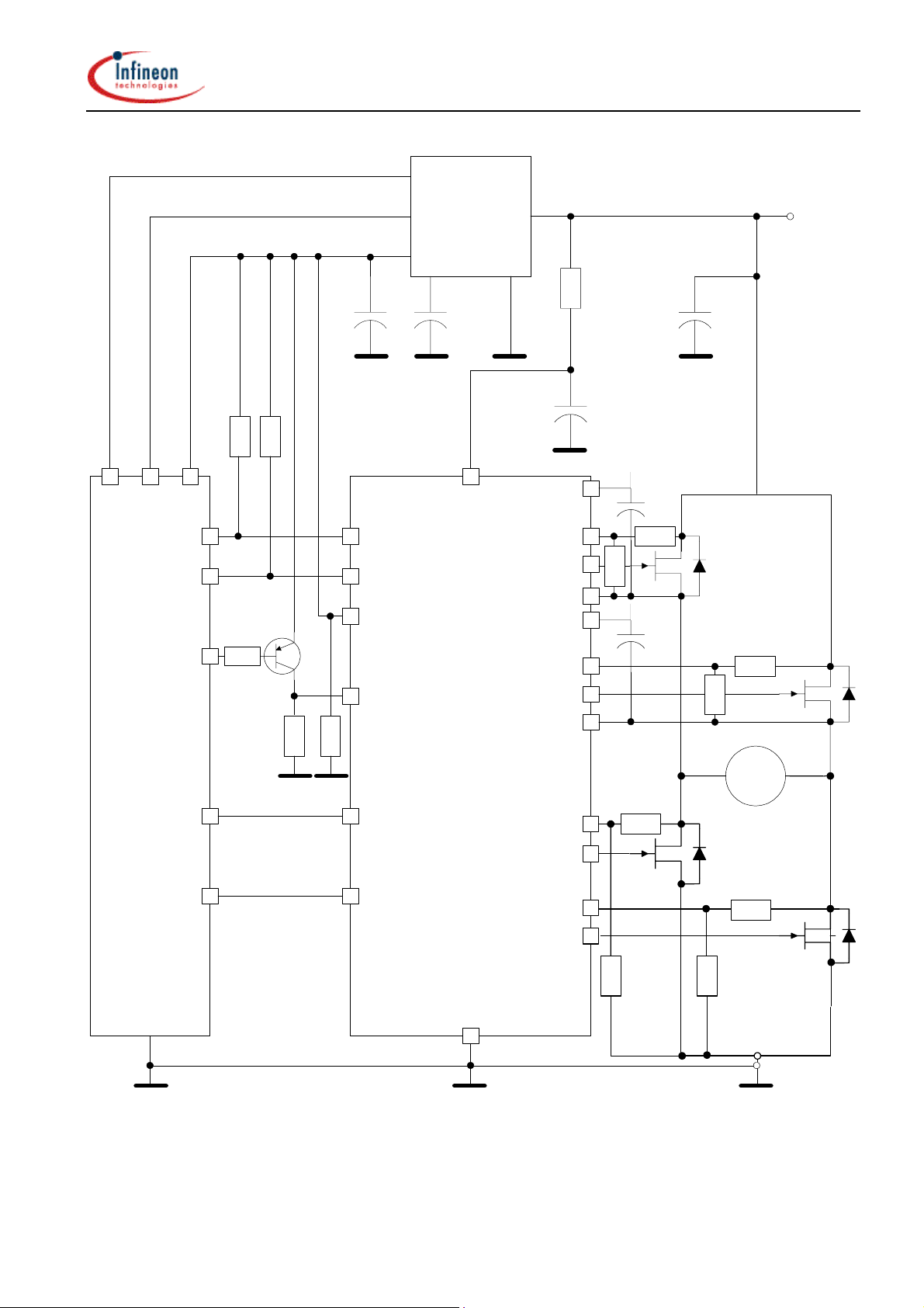
Application Block Diagram
Watchdog
WD R V
µC
R
Q
47kOhm
cc
68 kOhm
10kOhm
R
Q
= 47µF
C
s
R
Q
47kOhm
BCR192W
C
47µF
Q
DT / DIS
R
220k
Reset
Q
ER1
ER2
INH
INH
TLE
4278G
D
= 47nF
C
D
Vs
I
BH1
DH1
GH1
SH1
BH2
DH2
GH2
SH2
R = 10 Ohm
C
s
= 1µF
C
s
R
SCD
= 47µF
C
B
220nF
R
SCD
C
220nF
Vs = 12V
B
R
SCD
R
SCD
M
R
PWM
DL1
GL1
DIR
DL2
GL2
GND
This application block diagram shows one of the possibilities to use this Driver IC. The voltage devider networks accross the 4 MOSFETs (resistors R
limit threshold for Short Circuit protection. The R
the bootstrap capacitors. If R
resistors are not used in the application, a 12k Ohm resistor
SCD
resistors also provide a charge path for
SCD
SCD
should be introduced between SH1 to GND and SH2 to GND.
SCD1
R
SCD3
R
SCD2
R
SCD4
) allow to increas the current
2 2006-01-30
Page 3
Data Sheet TLE6284G
DT/DIS
ER1
DIR
PWM
DL2
VS
DL1
INH
1
1
2
2
3
3
4
4
5
5
6
6
7
7
8
8
9
9
10
10
TLE6284G
20
20
19
19
18
18
17
17
16
16
15
15
14
14
13
13
12
12
11
11
GL2
SH2
GH2
BH2
DH2
DH1 ER2
BH1 GND
GH1
SH1
GL1
Pin Symbol Function
1 DT / DIS a) Set adjustable dead time by external resistor
b) Reset ERx register
c) Disable output stages
2 ER1 Error flag for driver shut down
3 DIR Control input for spinning direction of the motor
4 PWM Control input for PWM frequency and duty cycle
5 DL2 Sense contact for short circuit detection low side 2
6 ER2 Warning flag Temperature / distinguish if short cir-
cuit or undervoltage lock out occured
7 GND Logic Ground
8 VS Voltage supply
9 DL1 Sense contact for short circuit detection low side 1
10
11 GL1 Output to gate low side switch 1
12 SH1 Connection to source high side switch 1
13 GH1 Output to gate high side switch 1
14 BH1 Bootstrap supply high side switch 1
15 DH1 Sense contact for short circuit detection high side 1
16 DH2 Sense contact for short circuit detection high side 2
17 BH2 Bootstrap supply high side switch 2
18 GH2 Output to gate high side switch 2
19 SH2 Connection to source high side switch 2
20 GL2 Output to gate low side switch 2
INH Sets complete device to sleep mode to achieve low
quiescent currents
3 2006-01-30
Page 4
Data Sheet TLE6284G
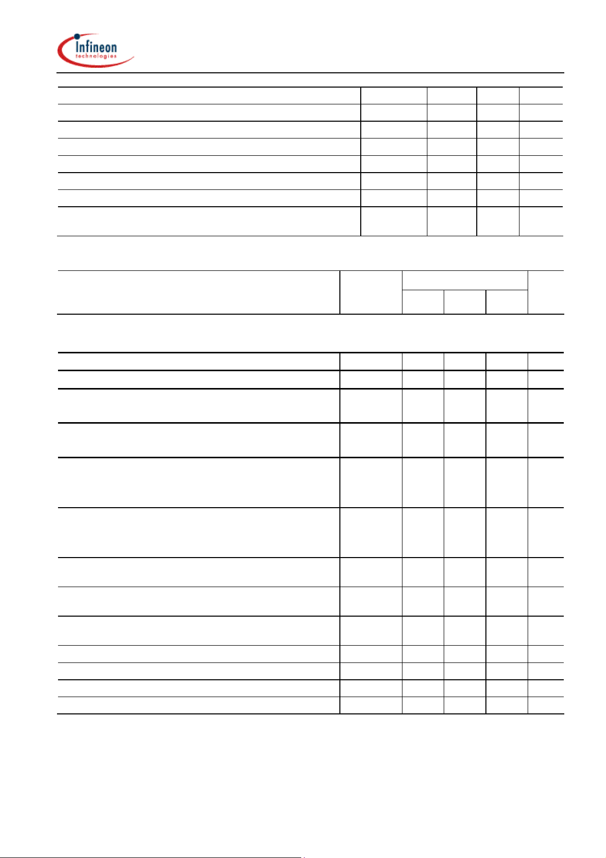
Maximum Ratings at Tj=-40…+150°C unless specified otherwise
Limits ValuesParameter Symbol
Unit
Min. Max.
Supply voltage 1 VS -4 60 V
Operating temperature range
Storage temperature range
Tj
T
stg
-40
-55
150
150
°C
Max. voltage range at PWM, DIR, DT/DIS -1 6V
Max. voltage range at ERx -0.3 6V
Max. voltage range at INH VINH -0.6 60 V
Max. voltage range at BHx VBHx -0.3 90 V
Max. voltage range at DHx
Max. voltage range at GHx
Max. voltage range at SHx
2
VDHx -4 75 V
3
VGHx -6.8 86 V
3
VSHx -6.8 75 V
Max. voltage range at GLx VGLx -2 12 V
Max. voltage range at DLx VDLx -2 75 V
Max. voltage difference BHx – SHx VBHx-VSHx -0.3 17 V
Max. voltage difference Gxx – Sxx VGxx-VSxx -0.3 11 V
Power dissipation (DC) @ TA=125°C / min.footprint P
Power dissipation (DC) @ TA=85°C / min.footprint P
Electrostatic discharge voltage (Human Body Model)
0.33 W
tot
0.85 W
tot
4
V
ESD
2kV
according to MIL STD 883D, method 3015.7 and
EOS/ESD assn. standard S5.1 – 1993
Jedec Level 3
Thermal resistance junction - ambient (minimal foot-
R
75 K/W
thJA
print with thermal vias)
Thermal resistance junction - ambient (6 cm2) R
75 K/W
thJA
Functional range
Parameter and Conditions Symbol Values Unit
at Tj = -40…+150°C, unless otherwise specified
min max
Supply voltage VS 7.5 60 V
Operating temperature range Tj -40 150 °C
Max. voltage range at PWM, DIR, DT/DIS -0.3 5.5 V
Max. voltage range at ERx -0.3 5.5 V
Max. voltage range at INH VINH -0.6 60 V
Max. voltage range at BHx VBHx -0.3 90 V
Max. voltage range at DHx2 VDHx -4 75 V
1
With external resistor (≥10 Ω ) and capacitor
2
The min value -4V is reduced to –( V
3
The min value -7V is reduced to –(V
4
All test involving Gxx pins V
ESD
=1 kV!
BHx
BHx
- V
) in case of bootstrap voltages V
SHx
- V
- 1V) in case of bootstrap voltages V
SHx
BHx-VSHx
BHx-VSHx
<4V
<8V
4 2006-01-30
Page 5
Data Sheet TLE6284G
Max. voltage range at GHx3 VGHx -6.8 86 V
Max. voltage range at SHx3 VSHx -6.8 75 V
Max. voltage range at GLx VGLx -2 12 V
Max. voltage range at DLx VDLx -2 75 V
Max. voltage difference BHx – SHx VBHx-VSHx -0.3 12 V
Max. voltage difference Gxx – Sxx VGxx-VSxx -0.3 11 V
PWM frequency FPW M 0 50 kHz
Minimum on time external lowside switch – static con-
dition @ 20 kHz; Q
= 200nC
Gate
Electrical Characteristics
Parameter and Conditions Symbol Values Unit
at Tj = -40…150°C, unless otherwise specified
and supply voltage range V
Static Characteristics
S = 7.5 … 60V; f
= 20kHz
PWM
tp(min) 2µs
min typ max
Low level output voltage (VGSxx) @ I=10mA
High level output voltage (VGSxx) @ I=-10mA
Supply current at VS (device disabled)
@ V
= VS =14V R
bat
=400kΩ
DT
Supply current at VS (device disabled)
@ V
= VS =42V R
bat
=400kΩ
DT
Quiescent current at VS (device inhibited)
@ V
R
= VS =14V R
bat
SCD1+RSCD2
DT
= R
SCD3+RSCD4
=400kΩ
=12kΩ
Quiescent current at VS (device inhibited)
@ V
R
Supply current at VS @ V
f
PWM
Supply current at VS @ V
f
PWM
Supply current at VS @ V
f
PWM
= VS =42V R
bat
SCD1+RSCD2
= R
=400kΩ
DT
SCD3+RSCD4
= VS =14V,
bat
= 20kHz (Outputs open)
= VS =14V,
bat
= 50kHz (Outputs open)
= VS =42V,
bat
= 20kHz (Outputs open)
=12kΩ
∆
VLL -- 60 150 mV
∆
VHL 8 10 11 V
IVS(dis)14V -- 4 8 mA
IVS(dis)42V -- 4 8 mA
IVS(inh)14V -- 0.6 1.5 mA
IVS(inh)42V -- 0.6 1.5 mA
I
VS(open)14V
I
VS(open)14V
I
VS(open)42V
-- 7 15 mA
-- 7 15 mA
-- 7 15 mA
Low level input voltage VIN(LL) -- -- 1.0 V
High level input voltage VIN(HL) 2.0 -- -- V
Input hysteresis
Inhibit trip level V
∆
VIN 100 170 mV
1.3 2 3 V
INH
5 2006-01-30
Page 6

Data Sheet TLE6284G
Dynamic characteristics (pls. see test circuit and timing diagram)
Turn on current @ VGxx –VSxx = 0V; Tj=25°C
@ VGxx –VSxx = 4V; Tj=125°C
@ C
=22nF ; R
Load
load
= 0Ω
Turn off current @ VGxx –VSxx = 10V; Tj=25°C
@ VGxx –VSxx = 4V; Tj=125°C
@ C
= 22nF ; R
Load
load
=0Ω
Dead time (adjustable) @ RDT = 1 kΩ
@ RDT = 10 kΩ
@ R
@ R
@ C
Rise time @ C
Fall time @ C
=10nF ; R
Load
load
=10nF ; R
Load
=10nF ; R
Load
=1Ω
DT = 50 kΩ
DT = 200 kΩ
=1Ω (20% to 80%) t
load
=1Ω (80% to 20%) tfall -- 150 440 ns
load
Disable propagation time
@ C
=10nF ; R
Load
load
=1Ω
Reset time of diagnosis
@ C
=10nF ; R
Load
load
=1Ω
Input propagation time
(low side turns on, 0% to 10%)
Input propagation time
(low side turns off, 100% to 90%)
Input propagation time
(high side turns on, 0% to 10%)
Input propagation time
(high side turns off, 100% to 90%)
Input propagation time difference
(all channels turn on)
Input propagation time difference
(all channels turn off)
Input propagation time difference
(one channel; low on – high off)
Input propagation time difference
(one channel; high on – low off)
Input propagation time difference
(all channels; low on – high off)
Input propagation time difference
(all channels; high on – low off)
IGxx(on) --
IGxx(off) --
tDT --
0.05
0.40
--
--
--
850
700
580
300
0.01
0.20
1.0
3.1
--
--
----mA
--
0.38
2.50
--
mA
µs
-- 100 300 ns
rise
tP(DIS) 3.6 5 7 µs
tP(CL) 1 2 3.1 µs
tP(ILN) -- 250 500 ns
tP(ILF) -- 110 500 ns
tP(IHN) -- 200 500 ns
tP(IHF) -- 130 500 ns
tP(Diff) 20 50 70 ns
tP(Diff) -- 25 50 ns
tP(Diff) -- 120 180 ns
tP(Diff) -- 100 180 ns
tP(Diff) -- 120 180 ns
tP(Diff) -- 100 180 ns
6 2006-01-30
Page 7

Data Sheet TLE6284G
Test Circuit and Timing Diagram
x2
PWM
GHx
SHx
GLx
SLx
R
C
R
C
= 1 Ohm
load
= 10 nF
load
= 1 Ohm
load
= 10 nF
load
V
V
GHX_C
GLX_C
PWM
V
GHX_C
50%
t
t
t
P(IHN)
rise
80%
20%
10%
t
P(IHF)
t
fall
90%
t
t
t
P(ILF)
fall
t
t
P(ILN)
rise
V
Test Conditions :
GLX_C
Junction temperature Tj = -40 … 150oC
Supply voltage range Vs = 7.5 … 60V
PWM frequency f
= 20 kHz
PWM
Diagnosis and Protection Functions
Overtemperature warning T
Hysteresis for overtemperature warning ∆T
Short circuit protection filter time t
Short circuit criteria (VDS of Mosfets)
SCP(off)
V
For Low sides
For High sides
Disable input level V
Disable input hysteresis ∆V
Error level @ 1.6mA I
Under voltage lock out for highside output – boot-
V
ERx
V
strap voltage
Under voltage lock out for lowside output –
V
supply voltage
90%
80%
20%
150 170 190 °C
J(OV)
20 °C
J(OV)
6 9 12 µs
DS(SCP)
0.5
0.45
3.3 3.7 4.0 V
DIS
180 mV
DIS
-- -- 1.0 V
ERx
BHx (uvlo)
Vs (uvlo)
3.7 4.6 V
4.8
0.75
0.75
1.0
1.05
5.9 V
10%
t
V
7 2006-01-30
Page 8

Data Sheet TLE6284G
Remarks:
Default status of input pins:
To assure a defined status of the logic input pins in case of disconnection, these pins are
internally secured by pull up / pull down current sources with approx. 20µA. The high voltage
proof input INH should be secured by an external pull down resistor close to the device. The
following table shows the default status of the logic input pins.
Input pin Default status
PWM and DIR Low (= break in high side)
DT/DIS (active high) High
Definition:
In this datasheet a duty cycle of 98% means that the GLx pin is 2% of the PWM period in
high condition.
Remark: Please consider the influence of the dead time and the propagation time differences for the input duty cycle
Functional description
Description of Dead Time Pin / Disable Pin / Reset
This pin allows to adjust the internal generated dead time. The dead time protects the external highside and lowside Mosfets in the same halfbridge against a lowohmic connection between battery and GND and the resulting cross current through these Mosfets. The adjustable dead time allows to minimize the power dissipation caused by the current flowing
through the body diode during switching the halfbridge.
In addition this pin allows to reset the diagnosis registers without shut down of any output
stage as well as the possibility to shut down all outputs simultaneously.
Condition of DT/DIS pin Function
0 - 3.5V Adjust dead time between 10ns and 3.1µs
> 4V
Description of Inhibit functionality
In automotive applications which are permanently connected to the battery line, it is very important to reduce the current consumption of the single devices. Therefore the TLE6284G
offers a inhibit mode to put the device to sleep and asure very low quiescent currents. To
deactivate the inhibit mode the INH pin has to be set to high. This can be done by connecting this pin to voltages between 3.3 and 60V without external protection. An inhibit mode
means a complete reinitialisation of the device.
Description of Diagnosis
The two ERx pins are open collector outputs and have to be pulled up with external pull up
resitors to 5V. In normal conditions both ERx signals are high. In case of shutdown of any
output stage the ER1 is pulled down. This shut down can be caused by undervoltage or
short circuit. In this condition ER2 indicates the reason for the shut down.
a) Reset of diagnosis register if DT/DIS voltage is higher than
4V for a time between 3.1µs and 3.6µs
b) Shut down of output stages if DT/DIS voltage is higher
than 4V for a time above 7µs (Active pull down of gate voltage)
8 2006-01-30
Page 9

Data Sheet TLE6284G
Condition of
ER1 pin
5V 5V no errors
5V 0V overtemperature warning of driver IC
0V 5V Shut down of any output stage caused by short circuit
0V 0V Shut down of any output stage caused by undervoltage
Recommended Start-up procedure
The following procedure is recommended whenever the Driver IC is powered up:
• Disable the Driver IC via DT/DIS pin
• Wait until the bootstrap capacitors of High Side MOSFET C
time depends on application conditions, e.g. CBx and RBx)
• Enable the Driver IC via DT/DIS pin
• Start the operation by applying the desired pulse patterns. Do not apply any pulse pat-
terns to the PWM or DIR pin, before the CBx capacitors are charged up.
Short Circuit protection
The current threshold limit to activate the Short Circuit protection function can be adjusted to
larger values, it can not be adjusted to lower values. This can be done by external resistors
to form voltage deviders across the “sense element” (pls. see Application block diagram on
pg. 2), consisting of the Drain-Source-Terminals, a fraction of the PCB trace and – in some
cases – current sense resistors (used by the µC not by the Driver IC).
The Short Circuit protection can be disabled for the High Side MOSFETs by shorting DH1
with SH1 and DH2 with SH2 on the PCB; in this case the DHx pins may not be connected to
the Drains of the associated MOSFETs. To disable Short Circuit protection for the Low Side
MOSFETs the DL1 and DL2 pin should be connected to the Driver IC´s Ground.
Shut down of the driver
A shut down can be caused by undervoltage or short circuit.
A short circuit will shut down only the affected Mosfet until a reset of the error register by a
disable of the driver occurs. A shut down due to short circuit will occur only when the Short
Circuit criteria V
t
SCP(off)
. Yet, the exposure to or above V
tive Short Circuit conditions shorter than t
MOSFET.
An undervoltage shut down shuts only the affected output down. The affected output will
auto restart after the undervoltage situation is over.
Operation at Vs<12V
If Vs<11.5V the gate voltage will not reach 10V. It will reach approx Vs-1.5V, dependant on
duty cyle, bootstrap capacitor, total gate charge of the external Mosfet and switching frequency.
Operation at different voltages for Vs, DH1 and DH2
If DH1 and DH2 are used with a voltage higher than Vs, a duty cycle of 100% can not be
guaranteed. In this case the driver is acting like a normal driver IC based on the bootstrap
principle. This means that after a maximum “On” time of the highside switch of more than
1ms a refresh pulse to charge the bootstrap capacitor of about 1µs is needed to avoid undervoltage lock out of this output stage.
Condition of
ER2 pin
DS(SCP)
is met for a duration equal to or longer than the Short Circuit filter time
Function
DS(SCP)
scp(off)
are charged (the waiting
Bx
is not counted or accumulated. Hence, repeti-
will not result in a shut down of the affected
9 2006-01-30
Page 10

Data Sheet TLE6284G
Operation at extreme duty cycle:
The integrated charge pump allows an operation at 100% duty cycle. The charge pump is
strong enough to replace leakage currents during “on”-phase of the highside switch. The
gate charge for fast switching of the highside switches is supplied by the bootstrap capacitors. This means, that the bootstrap capacitor needs a minimum charging time of about 1ms,
if the highside switch is operated in PWM mode (e.g. with 20kHz a maximum duty cycle of
96% can be reached). The exact value for the upper limit is given by the RC time formed by
the impedance of the internal bootstrap diode and the capacitor formed by the external Mosfet (C
Mosfet=QGate
MOSFET the driver IC has to drive. Usually the bootstrap capacitor is about 10-20 times bigger then C
Mosfet
The charge pump is active when the highside switch is “ON” and the voltage level at the SHx
is higher than 4V. Only under these conditions the bootstrap capacitor is charged by the
charge pump.
Estimation of power loss within the Driver IC
The power loss within the Driver IC is strongly dependent on the use of the driver and the
external components. Nevertheless a rough estimation of the worst case power loss is possible. Worst case calculation is:
P
= (Q
Loss
gate
With:
P
= Power loss within the Driver IC
Loss
f
= Switching freqency
PWM
Q
= Total gate charge of used MOSFETs at 10V VGS
gate
n = Number of switched MOSFETs
const = Constant considering some leakage current in the driver (about 1.2)
I
VS(open)
= Current consumption of driver without connected Mosfets during switching
VVS = Voltage at Vs
P
= Power dissipation in the external gate resistors
RGate
This value can be reduced dramatically by usage of external gate resistors.
/ VGS). The size of the bootstrap capacitor has to be adapted to the external
. External components at the Vs Pin have to be considered, too.
*n*const* f
PWM
+ I
VS(open)
/20kHz)* VVs - P
RGate
Estimated Power Lo ss P
0,8
0,7
0,6
0,5
(W)
0,4
LOSS
0,3
P
0,2
0,1
0
0 102030405060
Conditions
Junction temperature Tj = 25oC
Number of switched MOSFET n = 2
Power dissipation in the external gate resistors P
for different supply voltages V
LOSS
at QG = 100nC @ VGS = 10V
Vs = 8V
Vs = 14V
Vs = 18V
PWM Frequency (kHz)
:
with in the Driv er IC
s
Estimated Power Loss P
for different gate charges Q
at sup ply voltage Vs = 14V
0,8
0,7
0,6
0,5
(W)
0,4
LOSS
0,3
P
0,2
0,1
0
0 102030405060
RGate
QG = 50nC
= 100nC
Q
G
= 200nC
Q
G
PWM Frequency (kHz)
= 0,2*P
within the Driver IC
LOSS
Loss
G
10 2006-01-30
Page 11

Data Sheet TLE6284G
Gate Drive characteristics
Logic
+
V
PWM_HS
Level
Shift
+
V
GS
limit
+
Under
voltage
SCD
i
Gxx(on)
i
Gxx(off)
BHx
DHx
GHx
SHx
C
i
GHx
V
PWM_HS
V
s
i
Gxx(on)
850 mA Peak
B
i
Gxx(off)
580 mA Peak
Motor
TLE6284G
High Side Driver
- Turn Off : V
Test Conditions :
- Turn On : V
= 0V, Tj = 25oC
GS
= 10V, Tj = 25oC
GS
This figure represents the simplified internal
circuit of one high side gate drive. The drive
circuit of the low sides look similar.
i
GHx
This figure illustrates typical voltage and
current waveforms of the high side gate drive;
the associated waveforms of the low side
drives look similar.
11 2006-01-30
Page 12

Data Sheet TLE6284G
Truth Table
Input Conditions Output driver IC Output
Bridge
DIR PWM DT / DIS UV OT SC GH1 GL1 GH2 GL2 ER1 ER2 Out1 Out2
0
1
<3.5V 0 0 0 1 0 0 1
0 0 <3.5V 0 0 0 1 0 1 0
1 1 <3.5V 0 0 0 0 1 1 0
1 0 <3.5V 0 0 0 1 0 1 0
0
1
<3.5V 1 0 0 B 0 0 B
0 0 <3.5V 1 0 0 B 0 B 0
1 1 <3.5V 1 0 0 0 B B 0
1 0 <3.5V 1 0 0 B 0 B 0
0
1
<3.5V 0 1 0 1 0 0 1
0 0 <3.5V 0 1 0 1 0 1 0
1 1 <3.5V 0 1 0 0 1 1 0
1 0 <3.5V 0 1 0 1 0 1 0
0
1
<3.5V 0 0 1 E 0 0 E
0 0 <3.5V 0 0 1 E 0 E 0
1 1 <3.5V 0 0 1 0 E E 0
5V 5V 1 0
5V 5V 1 1
5V 5V 0 1
5V 5V 1 1
C D 1
C D 1
A
0 A
A
1 A
C D 0 A 1 A
C D 1 A 1 A
5V 0V 1 0
5V 0V 1 1
5V 0V 0 1
5V 0V 1 1
F 5V 1
A
0 A
F 5V 1 A 1 A
F 5V 0 A 1 A
1 0 <3.5V 0 0 1 E 0 E 0
X
X
X X X X 0 0 0 0
X X >4V X X X 0 0 0 0
F 5V 1 A 1 A
5V 5V T T
5V 5V T T
A) Tristate when affected by undervoltage shut down or short circuit
B) 0 when affected; 1 when not affected; self recovery
C) 0V when output does not correspond to input patterns; 5V when output corresponds to
input patterns
D) Is an output affected by undervoltage ER2 is 0V
E) 0 when affected– the outputs of the affected halfbridge are shut down and stay latched
until reset; 1 when not affected
F) 0V when output does not correspond to input patterns – the outputs of the affected half-
bridge are shut down and stay latched until reset; 5V when output corresponds to input
patterns.
T) Tristate
X) Condition has no influence
Remark: To generate fast decay control mode, set PWM to 1 and send pwm-pattern to DIR
input.
12 2006-01-30
Page 13

Data Sheet TLE6284G
Driving Sequence and current flow in the MOSFETs and the motor
t
PWM
t
GL1
V
GH2
V
t
t
DIR
V
t
GH1
t
GL2
V
t
Vs
Vs
Vs
Vs
Vs
Vs
Acceleration Motor turns right Motor stops Motor turns left Motor stops
motor
I
M
M
M
M
M
M
13 2006-01-30
Page 14

Data Sheet TLE6284G
Package and Ordering Code
(all dimensions in mm)5
Package Code
P-DSO 20
5
For detailed information about packages please contact
http://www.infineon.com/cgi/ecrm.dll/ecrm/scripts/pack_cat.jsp?oid=-8781
14 2006-01-30
Page 15

Data Sheet TLE6284G
Published by
Infineon Technologies AG,
Bereich Kommunikation
St.-Martin-Strasse 53,
D-81541 München
© Infineon Technologies AG 1999
All Rights Reserved.
Attention please!
The information herein is given to describe certain components and shall not be considered as warranted characteristics.
Terms of delivery and rights to technical change reserved.
We hereby disclaim any and all warranties, including but not limited to warranties of non-infringement, regarding
circuits, descriptions and charts stated herein.
Infineon Technologies is an approved CECC manufacturer.
Information
For further information on technology, delivery terms and conditions and prices please contact your nearest Infineon Technologies Office in Germany or our Infineon Technologies Representatives worldwide (see address
list).
Warnings
Due to technical requirements components may contain dangerous substances. For information on the types in
question please contact your nearest Infineon Technologies Office.
Infineon Technologies Components may only be used in life-support devices or systems with the express written
approval of Infineon Technologies, if a failure of such components can reasonably be expected to cause the failure of that life-support device or system, or to affect the safety or effectiveness of that device or system. Life
support devices or systems are intended to be implanted in the human body, or to support and/or maintain and
sustain and/or protect human life. If they fail, it is reasonable to assume that the health of the user or other persons may be endangered.
15 2006-01-30
 Loading...