

Page 1
Smart Quad Channel Low-Side Switch TLE 5216 G
SPT-IC
Features
• Overload protection
• Short circuit protection
• Cascadeable serial diagnostic interface
• Overvoltage protection
• µC compatible input
• Electrostatic discharge (ESD) protection
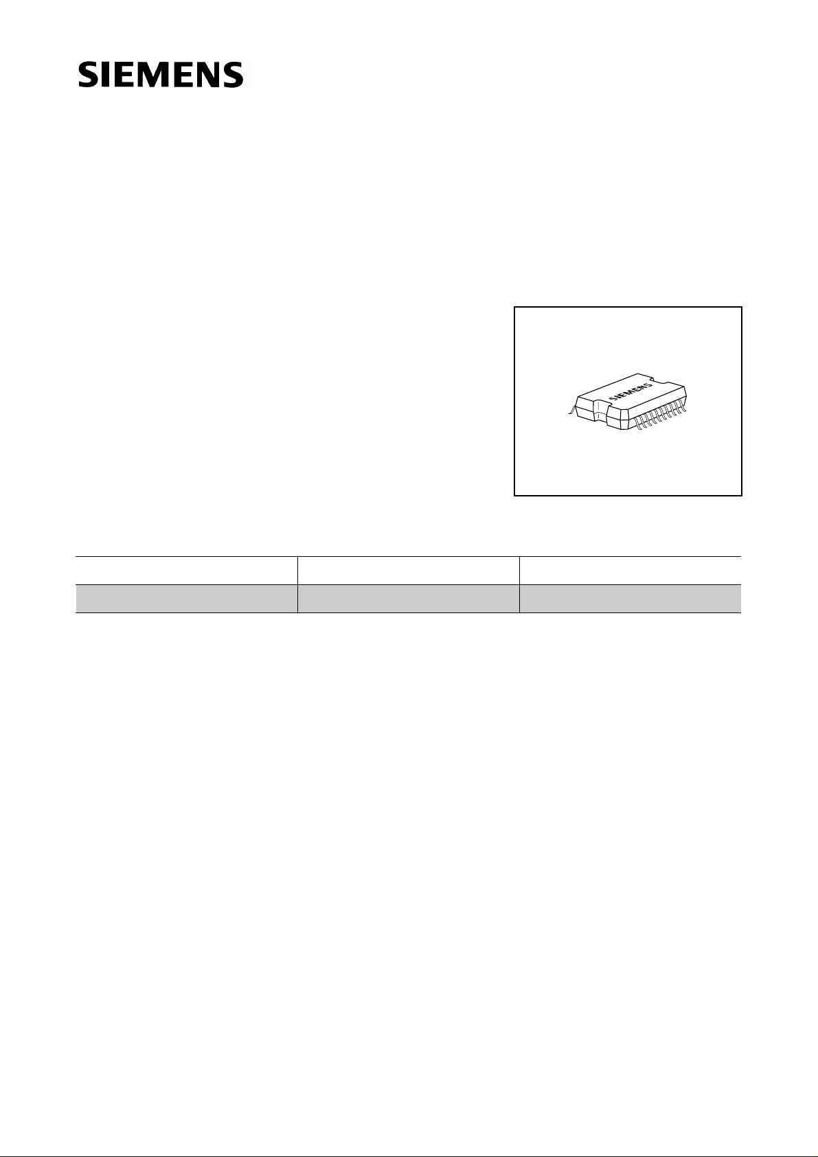
P-DSO-20-10
Type Ordering Code Package
▼
TLE 5216 G Q67006-A9206 P-DSO-20-10
▼ New Type
Application
• All kinds of resistive and inductive loads (relays, electromagnetic valves)
• µC compatible power switch for 12 V applications
• Solenoid control switch in automotive and industrial control systems
Semiconductor Group 1 1998-06-22
Page 2
TLE 5216 G
General Description
Quad channel Low-Side Switch in Smart Power Technology (SPT) with four separate
LOW active inputs and four open drain DMOS output stages. The TLE 5216G is
protected by embedded protection functions and designed for automotive and industrial
applications.
Product Summary
Parameter Symbol Values Unit
Supply voltage
Drain source clamping voltage
(OUT1 - OUT4)
ON resistance
Output current
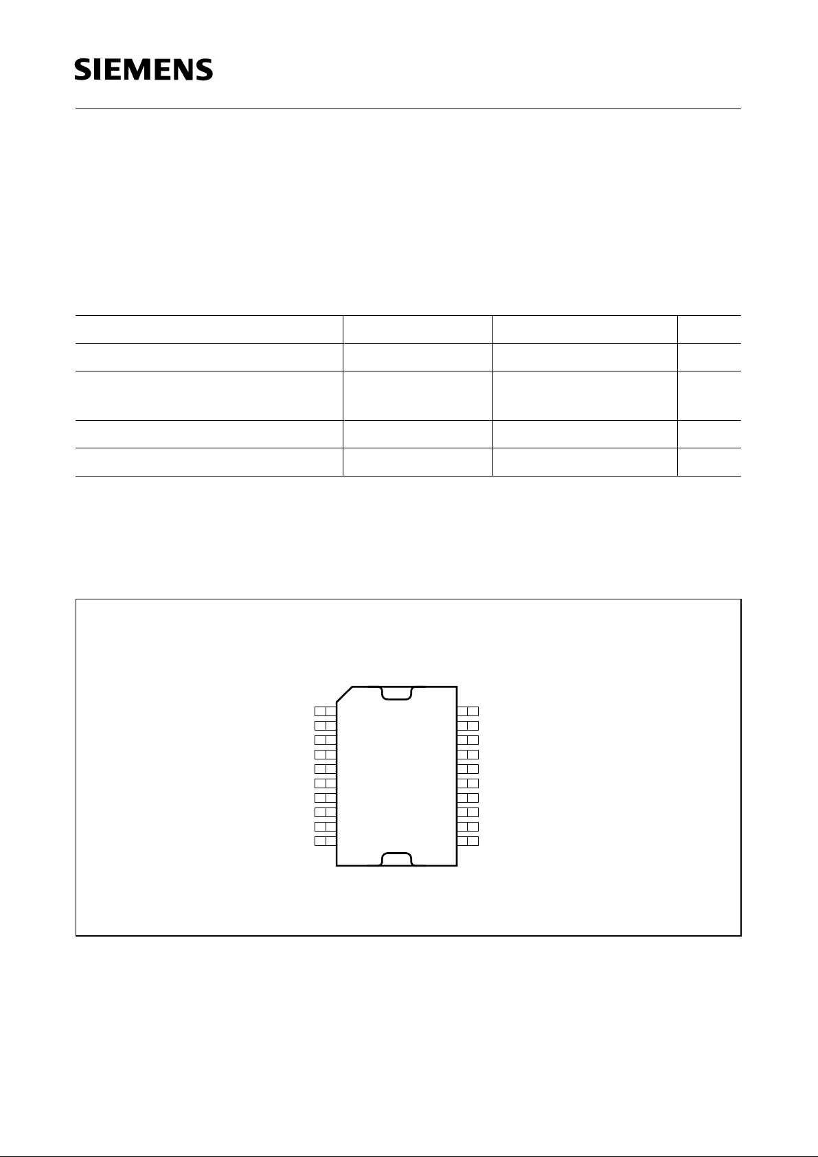
Pin Configuration
(top view)
GND
N.C.
IN1
IN2
OUT1
V
SEROUT SERIN
GND
V
V
R
I
D
P-DSO-20-10
1
2
3
4
5
6
S
7
8
9
10
S
DS(AZ)max
ON(typ)
20
19
18
17
16
15
14
13
12CLK
11
6 … 30 V
75 V
0.35 Ω
4 × 2A
GND
N.C.
IN4
IN3
OUT4
RESET
OUT3OUT2
CS
GND
AEP01617
Figure 1
Semiconductor Group 2 1998-06-22
Page 3
TLE 5216 G
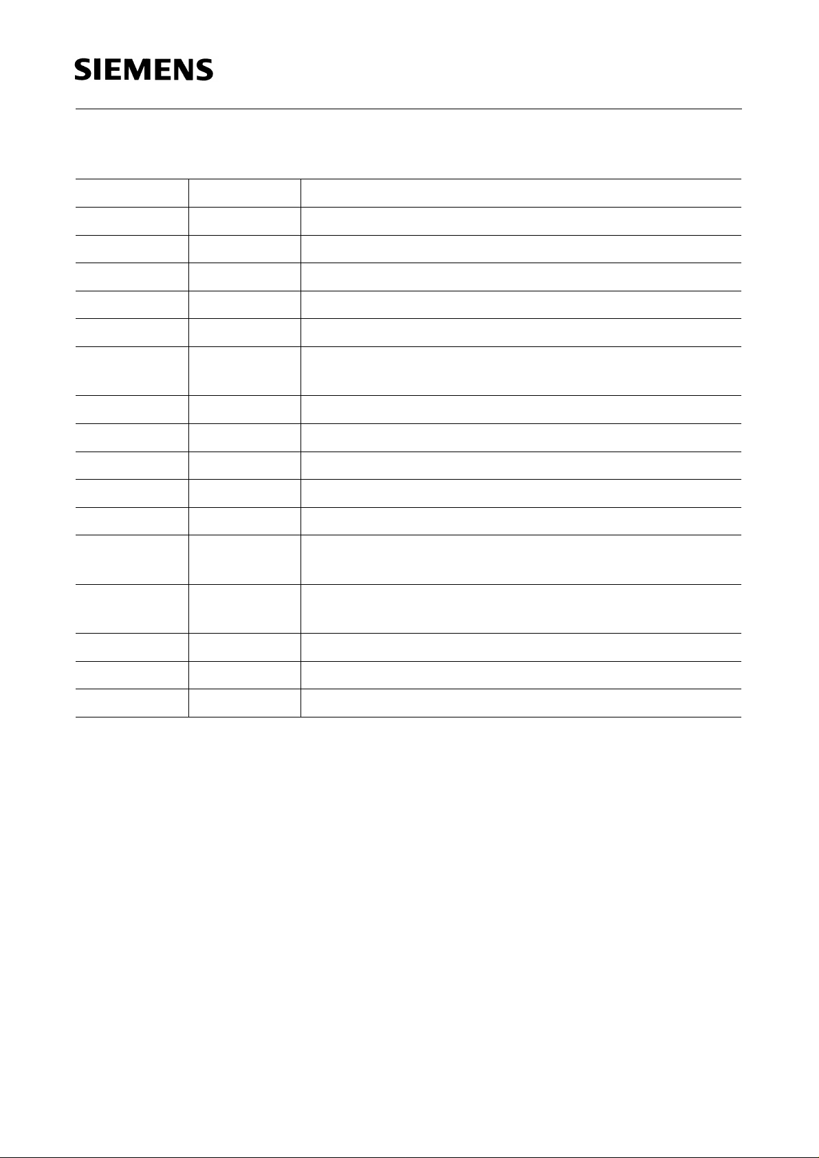
Pin Definitions and Functions
Pin No. Symbol Function
3 IN1 Input switch 1; active LOW; internal pull-up
4 IN2 Input switch 2; active LOW; internal pull-up
5 OUT1 Output switch 1; overload and shorted load protected
6
V
S
Supply voltage
7 OUT2 Output switch 2; overload and shorted load protected
8 SEROUT Data-out of serial diagnostic interface;
open drain
9 CLK Clock for serial diagnostic interface
1, 10, 11, 20 GND Ground
12 CS Chip select for serial diagnostic interface; internal pull-up
13 SERIN Data-in of serial diagnostic interface; internal pull-up
14 OUT3 Output switch 3; overload and shorted load protected
15 RESET Reset; active LOW; shuts down all outputs and resets
the error flags
16 OUT4 Output switch 4;
overload and shorted load protected
17 IN3 Input switch 3; active LOW; internal pull-up
18 IN4 Input switch 4; active LOW; internal pull-up
2, 19 N.C. Not connected
Semiconductor Group 3 1998-06-22
Page 4
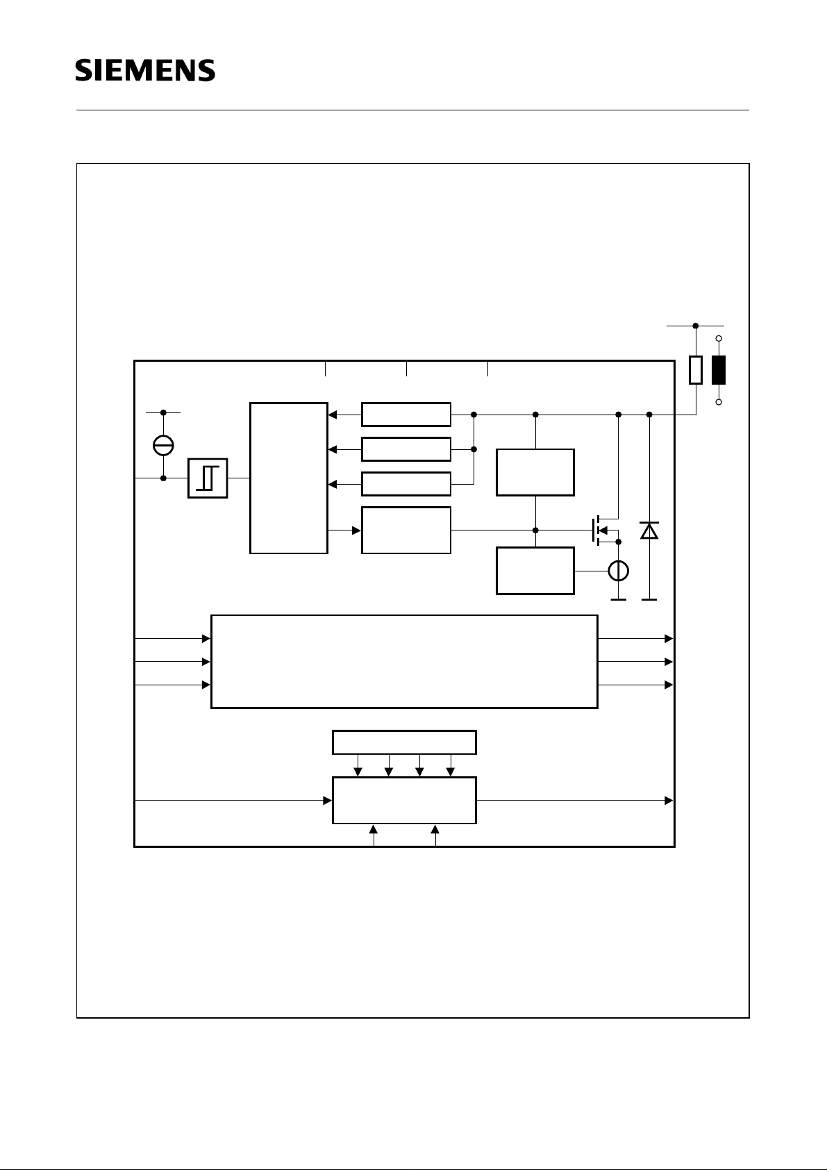
TLE 5216 G
V
BB
V
S
GNDRESET
TLE 5216 G
V
Internal
Overload
OUT1
Open Load
Clamp
Regulator
IN1
Logic
Channel 1
Short to GND
dv/dt Circuit
Current
Limit
IN2
IN3
IN4
Logic, Protection- and Power-Circuit of Channel 2-4
(equivalent to Channel 1)
OUT2
OUT3
OUT4
Logic Channel 1-4
SERIN SEROUT
Serial Diagnostic
Interface
CS CLK
AES02013
Figure 2
Block Diagram
Semiconductor Group 4 1998-06-22
Page 5

TLE 5216 G
Application Description
This IC is specially designed to drive inductive loads up to 2 A nominal current (valves,
relays, etc.). Integrated clamp-diodes limit the output voltage when inductive loads are
turned off.
For the detection of errors at the load there is a serial diagnostic interface, which
monitors the following errors for every output separately:
– open load in inactive mode
– shorted output (shorted to ground) in inactive mode
– overload or shorted load in active mode
Circuit Description
The block diagram shows the four independent power drivers with the referring logic
block and the serial diagnostic interface which stores and transfers the diagnostic
signals to the external circuit. Each power switch connects a high side load to ground
when a LOW signal applies at the inputs. To protect the IC against short circuit and over
load each output is provided with a current limitation and a delayed overload shutdown.
The slew rate of the switching process is limited internally.
The integrated clamp diodes limit the voltage at the output to
V
, when inductive
DS(AZ)
loads are switched off. The maximum power dissipation, which is given from the static
and dynamic thermal resistance, limits the allowable inductive energy. A diode in parallel
to every output clamps negative voltage.
All outputs, preferably the outputs 1 and 2 and the outputs 3 and 4 may be used in
parallel (no addition of max. freewheeling energy).
A curve of the output voltage is shown in figure 6.
The diagnostic block monitors the voltages across the power switch. If in active mode
(LOW level input) there is a higher voltage than
V
for a time longer than t
DS(OV)
VDS(OV)
, the
diagnostic block will show an overload in the error register and the affected power switch
will be shut off. The switch can only be reactivated if the corresponding input is switched
off and then on again.
In inactive mode (HIGH level at input) open load or shorted output (shorted load to
ground) is detected and signalled to the serial diagnostic interface. If the voltage across
the power switch is lower than
identified. If the voltage is even lower than
V
DS(OL)
for the time t
V
for the time t
DS(SH)
VDS(OL)
(min. 50 µs) open load is
VDS(SH)
(min. 30 µs)
"shorted to ground" is detected. An internal voltage divider will pull the output to the
voltage
V
if there is an open load.
DS
A new error on the same output stage will over-write the old error report. The protocol of
the serial diagnostic interface includes independent error reports for each output driver.
As soon as an error is latched into the error register the serial data output (SEROUT) of
the interface will go LOW (while CS is still HIGH). If the chip select gets a LOW signal
Semiconductor Group 5 1998-06-22
Page 6
TLE 5216 G
(CS = L), all error reports can be shifted out serially. The rising edge of the CS will reset
all error registers. The function of the serial diagnostic interface is shown in figure 7.
The data input (SERIN) allows several TLE 5216 G or other serial diagnostic interfaces
to be cascaded.
A LOW signal on the reset pin (RESET) or a supply voltage lower than the operating
range (4.5 V) will erase the error register and disable all four power switches.
Absolute Maximum Ratings
T
= – 40 °C to 150 °C
j
Parameter Symbol Values Unit
Supply voltage
Input voltages IN1 … IN4, SERIN, CLK, CS, RESET
Status output voltage Data OUT (SEROUT)
Operating temperature range
Storage temperature range
Output current per channel
Ground pin current
T
= 25 °C
j
T
= 125 °C
j
T
= 25 °C
j
T
= 125 °C
j
V
S
V
IN
V
SEROUT
T
j
T
Stg
I
D(AZ)
I
D(AZ)
I
GND
I
GND
– 2…40 V
– 0.3 … 7 V
– 0.3 … 10 V
– 40 … 150 °C
– 50 … 150 °C
– 3.8 … 3.8
– 2.95 … 2.95AA
– 10 … 10
– 8…8
A
A
Thermal resistance (junction-case static)
See diagrams P-DSO-20-10
R
thJC
5 K/W
Transient thermal impendance
t
= 100 µs; square pulse
p
t
= 100 µs; triangle pulse
p
Z
thJC
Z
thJC
0.5
0.2
K/W
K/W
Note: Maximum ratings are absolute ratings; exceeding only one of these values may
cause irreversible damage to the integrated circuit.
Semiconductor Group 6 1998-06-22
Page 7

TLE 5216 G
Operating Range
Parameter Symbol Limit Values Unit
min. max.
Supply voltage
V
S
630V
Supply voltage
outputs switchable; no diagnostic
Input LOW voltage
Input HIGH voltage
Clock input HIGH voltage
Inverse current at output
V
> 6 V V
S
V
> 6 V V
S
V
> 6 V V
S
V
> 6 V
S
isolated cooling fin
Junction temperature
Clock frequency
Clock pulse width
CS pulse width
Setup time CS to CLK
1)
If inverse current occurs at output 2 or 3, then provide external pull-up resistor 5.6 kΩ to + 5 V at input DIN.
V
> 6 V f
S
V
> 6 V t
S
V
> 6 V t
S
V
> 6 V t
S
V
I
1)
T
S
INL
INH
CLKH
D
j
CLK
CLKH,tCLKL
CSH,tCSL
CSC
4.5 V
– 0.3 1 V
26V
2.4 6 V
– 0.3 A
– 40 150 °C
0 500 kHz
400 ns
2 µs
2 µs
Note: In the operating range the functions given in the circuit description are fulfilled.
Semiconductor Group 7 1998-06-22
Page 8

TLE 5216 G
Electrical Characteristics
V
= 6 V to 18 V; Tj = – 40 °C to 150 °C (unless otherwise specified)
S
Parameter Symbol Limit Values Unit
min. typ. max.
Power Supply (
V
)
S
Supply current Outputs ON
Outputs OFF
Power Outputs
ON state resistance
T
=25°C; ID = 2 A; all VDS > 0 V
j
T
= 125 °C; ID = 1.5 A; t > 100 µs
j
Clamping voltage (OUT1 - OUT4)
I
= 1 A; 0 < Tj < 125 °C; all VDS > 0 V V
D
Negative clamping voltage
T
=25°C; ID = – 0.3 A V
j
Current limitation
T
=0°C; VDS = V
j
T
=25°C; VDS = V
j
T
= 125 °C; VDS = V
j
DS (OV)
DS (OV)
DS (OV)
Leakage current
V
= 0 V; VDS = 12 V; all VDS > 0 V I
S
I
S
I
S
R
DS(ON)
R
DS(ON)
DS(AZ)
DS(AZ)
I
D(lim)
I
D(lim)
I
D(lim)
R
3.5
8
0.35
0.55
8
15mAmA
0.4
0.63ΩΩ
65 70 75 V
– 1 – 0.5 V
3.0
2.8
2.25
3.6
3.3
2.6
4.2
3.8
2.95
A
A
A
0.2 0.5 mA
Digital Inputs
Inputs IN1 … IN4, CS, SERIN
Input LOW current 0 V <
Input HIGH current
Input hysteresis
V
< 2 V I
IN
V
= 5 V I
IN
INL
INH
V
INHys
– 200 – 100 – 50 µA
–20 0 5 µA
0.5 0.6 V
Input Clock (CLK)
Input current 0 V < V
Input hysteresis
Semiconductor Group 8 1998-06-22
INCLK
< 5 V I
INCLK
V
INCLKHys
–20 2 5 µA
0.5 0.7 V
Page 9

TLE 5216 G
Electrical Characteristics (cont’d)
V
= 6 V to 18 V; Tj = – 40 °C to 150 °C (unless otherwise specified)
S
Parameter Symbol Limit Values Unit
min. typ. max.
Input Reset
V
Input current 0 V <
< 2 V I
INR
INR
–25 –10 –5 µA
Input hysteresis
V
INRHys
Input Currents in Case of Inverse Current at Output
Σ
I
= – 0.3 A; VS = 0 V; 0 V < VIN < 5 V
D
Inputs CLK, SEROUT, CS, SERIN
Inputs IN1 … IN4
Input RESET
I
IN
I
IN
I
IN
Timings
Data valid SEROUT after CLK
Output ON delay
Output OFF delay
Difference of delays
Output slew rate falling
no 100 % testing
R
= 12 Ω t
L
R
= 12 Ω t
L
R
= 12 Ω t
L
C
= 1 nF; 10 V → 2VS
L
t
DDA
DON
DOFF
DON
f
– t
0.5 0.6 V
0 150 400 ns
0 1.4 10 µs
0 2.4 10 µs
–3 –1 3 µs
DOFF
–15 –8 –5 V/µs
200 µA
100 µA
25 µA
Output slew rate rising
I
= 1 A; 5 V → 55 V S
D
r
10 14 20 V/µs
Diagnostic Output (SEROUT)
Output leakage current V
Output LOW voltage 0 V <
Semiconductor Group 9 1998-06-22
I
SEROUT
SEROUT
= 5 V I
< 1.6 mA V
SEROUTH
SEROUTL
05µA
0 0.2 0.5 V
Page 10

TLE 5216 G
Electrical Characteristics (cont’d)
V
= 6 V to 18 V; Tj = – 40 °C to 150 °C (unless otherwise specified)
S
Parameter Symbol Limit Values Unit
min. typ. max.
Diagnostic Functions
Overload threshold Output ON
Overload delay
V
= 12 V; VBB = 12 V t
S
V
DS(OV)
VDS(OV)
1.5 2 2.5 V
30 80 200 µs
Open load output voltage
V
= 6.5 V; outputs OFF
S
V
= 12.5 V
S
V
V
DS
DS
3.3
6.7
3.8
7.7
4.3
8.7VV
Differential open load output resistance
Open load threshold
Open load delay
outputs OFF
V
= 6.5 V; outputs OFF
S
V
= 12.5 V
S
V
= 12 V t
S
R
D
V
DS(OL)
V
DS(OL)
VDS(OL)
51540kΩ
4.3
9.3
4.7
10.2
5.211V
V
50 130 250 µs
Shorted to ground threshold
V
Shorted to ground delay
= 6.5 V; outputs OFF
S
V
= 12.5 V
S
V
= 12 V t
S
V
DS(SH)
V
DS(SH)
VDS(SH)
2.4
4.5
2.8
5.4
3.3
6.3VV
30 80 200 µs
Note: The listed characteristics are ensured over the operating range of the integrated
circuit. Typical characteristics specify mean values expected over the production
spread. If not otherwise specified, typical characteristics apply at
T
= 25°C and
A
the given supply voltage.
Semiconductor Group 10 1998-06-22
Page 11

Test Circuits
TLE 5216 G
V
BB
100
+
V
S
=
V
INH
=
Figure 3
Test Circuit 1
F
µ
IN
1
IN
2
IN
3
IN
4
V
S
TLE 5216 G
OUT
OUT
OUT
OUT
Ι
D1
1
Ι
D2
2
Ι
D3
3
Ι
D4
4
Load
RESET SERIN CS CLK SEROUT GND
5k
Ω
V
DS
V
(OUT4) (OUT3)
DS (OUT2)
V
DS (OUT1)
V
DS
+
=
5V
=
V
INL
AES01437
V
S
TLE 5216 G
OUT
OUT
OUT
OUT
Ω
1
2
3
4
12
3 mH
a
b
12
100
µ
F
+
=
V
IN
IN
IN
IN
1
2
3
4
RESET SERIN CS CLK SEROUT GND
1 nF
+
=
5V
AES01438
Figure 4
Test Circuit 2
Semiconductor Group 11 1998-06-22
Page 12

TLE 5216 G
Ι
S
100µF
IN
1
IN
2
+
=
186
V...
IN
IN
3
4
V
S
TLE 5216 G
OUT
OUT
OUT
OUT
Ω
12
1
12
Ω
2
12
Ω
3
12
Ω
4
Figure 5
Test Circuit 3
H
Input
L
V
DS
(OUT)
Output
Voltage
t
VDS (OV)
a
b
5V
RESET SERIN
+
=
CS
CLK SEROUT GND
V
DS (AZ)
AES01439
S
r
t
VDS (OL)VDS (OL)
t
DOFF
t
VDS (SH)
VDS (OL) DS (OL)
t
VDS (SH)
Vt
VV
DS (SH)DS (SH)
50%
V
Load
t
DON
S
f
"Over Load"
V
DS (OV)
0
"Shorted" "Open Load"
V
DS(AZ)
t
AED01442
Figure 6
Switching Waveforms with Inductive Loads
Semiconductor Group 12 1998-06-22
Page 13

TLE 5216 G
CSL
t
CSH
t
CLKH
CLK
f
1/
CLKL
t
DDA
t
Di4
Di4
Di3
Di2Di1
Di0
D7
D6D5
D4
HHHLLH
Normal Function
LL
Overload, Shorted Load
Open Load
Shorted to Ground
AED01445
to GroundLoad
Shorted Load
OpenOverload,
Di3
D3
D2D1
CSC
tt
V
t
<
L
Error
H
No Error
CS
H
CLK
DSET
t
L
DHOLD
t
H
Di1 Di2
Di0
L
SERIN
D0
V
t
L
H
SEROUT
12 43Power Output Assignment
Shorted LoadError
No
L
H
Error Code:
Figure 7
Serial Diagnostic Interface Timing Diagram
Semiconductor Group 13 1998-06-22
Page 14

Thermal Resistance for P-DSO-20-10
1
10
K/W
Z
th
0
10
5
-1
10
5
TLE 5216 G
AED01893
1 Switch
2 Switches
4 Switches
-2
10
-2 -1
10
10
Note: Thermal resistance is measured at
are equally loaded at the same time.
Tj1
P
(W)
V1
Tj2
(W)
P
V2
Tj3
(W)
P
V3
Tj4
0.4 K/W
0.2
mJ/K
0.4 K/W
0.2
mJ/K
0.4 K/W
0.2
mJ/K
0.4 K/W
0.8 K/W
0.6
mJ/K
0.8 K/W
0.6
mJ/K
0.8 K/W
0.6
mJ/K
0.8 K/W
0.8
mJ/K
0.8
mJ/K
0.8
mJ/K
0
10
T
= 25°C and
C
1.4 K/W
K/W
1
1.4 K/W
mJ/K
2
1.4 K/W
1
K/W
1.4 K/W
1
10
Pulse width (square)
T
= 45°C. Multiple switches
jpeak
2.4 K/W
2
mJ/K
2.4 K/W
15
K/W
2.4 K/W
2.4 K/W
2
15
K/W
mJ/K
ms555
10
0.75 K/W
2
(W)
P
V4
0.2
mJ/K
0.6
mJ/K
0.8
mJ/K
2
mJ/K
100
mJ/K
T
(K)
C
AES01895
Figure 8
Thermal Equivalent Circuit for P-DSO-20-10
Note: Thermal equivalent circuit is valid at
T
= 110°C and 110°C
C
with
T
–
T
≤
jmax
100 K add 25 % headroom for thermal non-uniformity.
C
Semiconductor Group 14 1998-06-22
<Tj<
130°C,
T
= 25°C and 25°C
C
Z
is 15 % higher. For high power transients
th
< Tj<
45°C. At
Page 15

TLE 5216 G
Definition of Dynamic Thermal Resistance
(triangle Pulse)
P
Z
= (
T
-
T
) /
1000
P
max
t
s
µ
t
AED01446
P
j
max
max
T
th
0
0 100µs
T
j
j
0
j max j 0
Maximum Freewheeling Energy for
Inductive Loads
C
T
C
=110
AED01447
C
=60
C
A
100
mJ
f
=
80
70
10 Hz
Hz50
60
50
Freewheeling Energy
40
100 Hz
=
f
Hz10
50 Hz
30
Hz100
20
10
0
0.0
0.5 1.0 1.5 2.0 2.5
Switching Current
T
Maximum Freewheeling Energy for Inductive Loads with Various Switches in
Parallel
T
= 110 °C, f = 10 Hz
C
40
mJ
30
20
Max. Freewheeling Energy
10
0
0
2 4
1 Switch
2 Switches
6 8
Switching Current
AED01448
3...4 Switches
A
10
Semiconductor Group 15 1998-06-22
Page 16

TLE 5216 G
Diagnostic Threshold versus
Supply Voltage
V
DS
V
S
Normal
Function
V
DS
(OL)
DS
DS
(SH)
Error:
Open Load
Open Load
Output Voltage
Error:
Shorted
to Ground
AED01443
V
V
6 12 18
V
Current Limitation versus
Temperature
5
Ι
D(lim)
A
4
3
2
1
V
S
0
-40
AED01444
max
min
150100500
C
T
j
V
S
*)
To
V
S S
RESET
SEROUTSERIN
GND
CLK
CS
1-41-4 1-4
5.6 k
To
LoadsLoads
CC
Ω
SERININSEROUT
OUT
V
CC
TLE 5216 G TLE 5216 G
Ω
k5.6
OUT IN
V
GND
RESET
CLK
CS
1-4
*) The capacitance depends on the inductance and current load of the supply.
Figure 9
Application Circuit
k3.3
4
Ω
4
A9-13
VV
CC
A1-4
Control 2.IC
A8
Diagnosis Chip select
A7
Diagnosis Clock
A6
Power On Reset
Microcontroller
i.e. SAB 80515
A5
Diagnosis Data In
Control 1.IC
AES01449
Semiconductor Group 16 1998-06-22
Page 17

Package Outlines
P-DSO-20-10
(Plastic Dual Small Outline Package)
1.2
-0.3
±0.1
15.74
1.27
+0.13
0.4
20
M
11
TLE 5216 G
1)
±0.15
11
+0.15
0
±0.1
3.25
3.5 max.
2.8
1.3
0.1
20x0.25
A
6.3
14.2
±0.3
B
+0.07
-0.02
0.25
Heatsink
±0.15
0.95
0.25MB
±3˚
5˚
Index Marking
101
1 x 45˚
15.9
A
1)
±0.15
1) Does not include plastic or metal protrusion of 0.15 max. per side
GPS05791
GPS05791
Sorts of Packing
Package outlines for tubes, trays etc. are contained in our
Data Book “Package Information”.
SMD = Surface Mounted Device
Dimensions in mm
Semiconductor Group 17 1998-06-22
 Loading...