

Page 1
Uni- and Bipolar Hall IC Switches for
Magnetic Field Applications
Features
• Temperature compensated magnetic performance
• Digital output signal
• For unipolar and alternating magnetic fields
• Large temperature range
• Protection against reversed polarity
• Output protection against electrical disturbances
Type Ordering Code Package
TLE 4905 G; TLE 4935 G
TLE 4935-2 G; TLE 4945-2 G
SOT-89
Bipolar IC
▼
TLE 4905 G Q62705-K402 SOT-89
TLE 4935 G Q62705-K404 SOT-89
▼
TLE 4935-2 G Q62705-K405 SOT-89
▼
TLE 4945-2 G Q62705-K403 SOT-89
▼
▼ New type
TLE 4905/35/35-2/45-2 (Unipolar/Bipolar Magnetic Field Switches) have been designed
specifically for automotive and industrial applications. Reverse polarity protection is
included on-chip as is output protection against negative voltage transients.
Typical applications are position/proximity indicators, brushless DC motor commutation,
rotational indexing etc.
Semiconductor Group 1 1998-04-29
Page 2

Pin Configuration
(top view)
±0.2
1
2.25
±0.2
TLE 4905 G; TLE 4935 G
TLE 4935-2 G; TLE 4945-2 G
Center of
sensitive area
123
Figure 1
Pin Definitions and Funtions
Pin No. Symbol Function
1
V
S
2 GND Ground
3QOutput
Supply volt age
AEP02150
Semiconductor Group 2 1998-04-29
Page 3

TLE 4905 G; TLE 4935 G
TLE 4935-2 G; TLE 4945-2 G
Circuit Description
The circuit includes Hall generator, amplifier and Schmitt-Trigger on one chip. The
internal reference provides the supply voltage for the components. A magnetic field
perpendicular to the chip surface induces a voltage at t he hall probe. This voltage is
amplified and switches a Schmitt-trigg er with open-collector output. A protec tion diode
against reverse power supply is integrated.
The output is protected against electrical disturbances.
Threshold
Generator
1
V
S
V
S
V
Ref
Figure 2 Block Diagram
Hall-
Generator
2
GND
Amplifier
Schmitt-
Trigger
Output
Stage
AEB01243
3
Q
Semiconductor Group 3 1998-04-29
Page 4
TLE 4905 G; TLE 4935 G
TLE 4935-2 G; TLE 4945-2 G
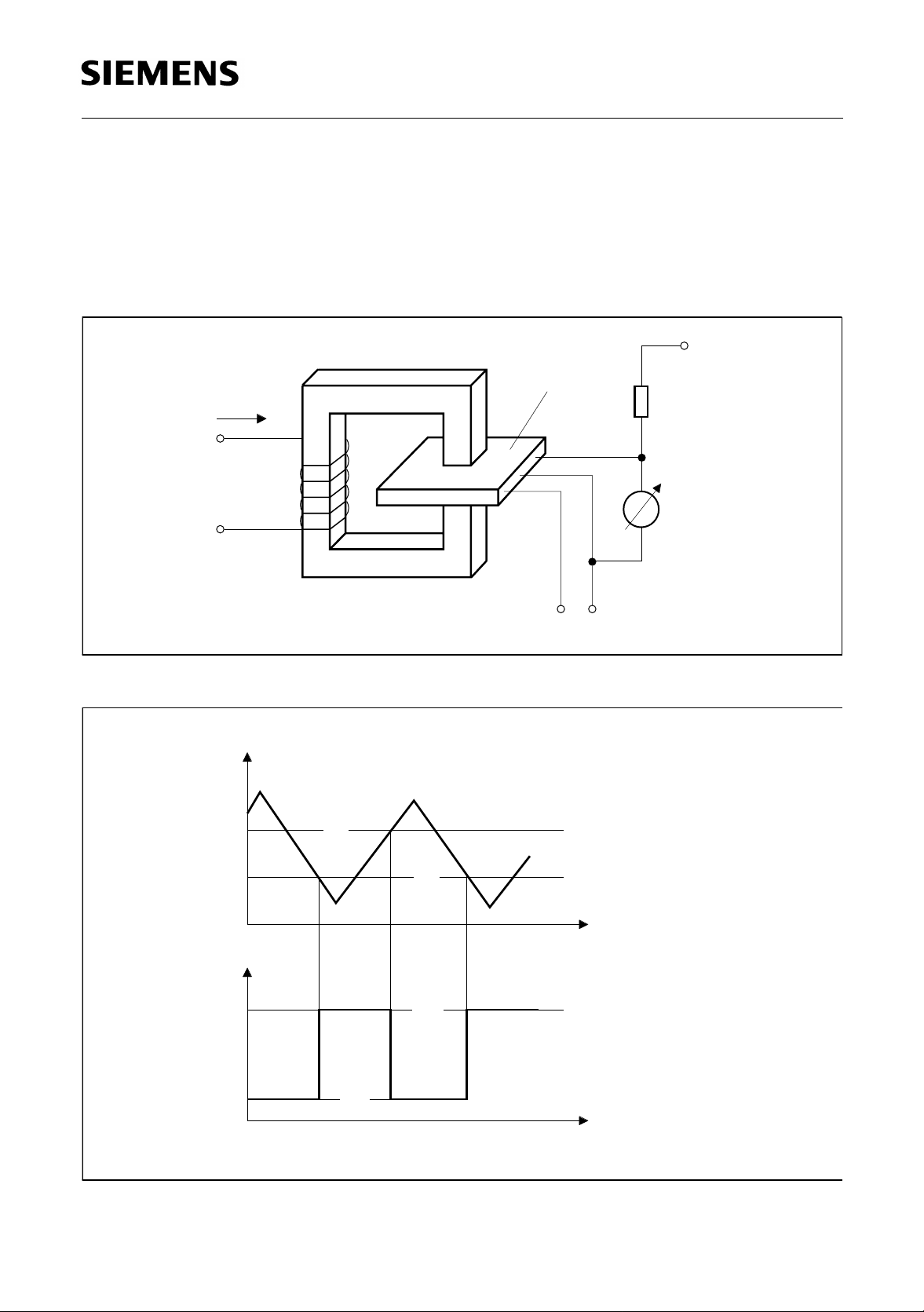
Functional Description Unipolar Type TLE 4905 (figure 3 and 4)
When a positive magnetic fie ld is applied in the indicated directi on (figure 3) and the
B
turn-on magnetic induction
(Operate Point). When the magnetic field is reduced to a value smaller than the release
point, the output of the IC turns off (Release Point; figure 4).
Ι
is exceeded, the output of the Hall-effect IC will conduct
OP
+
Branded Side
S
V
N
Q
Figure 3 Sensor/Magnetic-Field Configuration
B
B
OP
B
RP
0
V
Q
V
QH
+
-
V
S
Induction
t
Output Voltage
AES01231
V
QL
t
AED01420
Figure 4 Switching Characteristics Unipolar Type
Semiconductor Group 4 1998-04-29
Page 5

TLE 4905 G; TLE 4935 G
TLE 4935-2 G; TLE 4945-2 G
Functional Description Bipolar Type TLE 4935/35-2/45-2 (figure 5 and 6)
When a positive magnet ic field is applied in the indicated direction (figure 5) and the
B
turn-on magnetic induc tion
(Operate Point). The output state does not change unless a reverse magnetic field
exceeding the turn-of f ma gnetic induct ion |
turn off (Release Point; figure 6).
Ι
is exceeded, the outp ut o f the H all-e ffec t IC will conduct
OP
B
| is exceeded. In this case the output will
RP
+
Branded Side
S
N
Figure 5 Sensor/Magnetic-Field Configuration
B
B
OP
0
B
RP
V
Q
V
Q
+
-
V
S
t
AES01231
Induction
V
QH
Output Voltage
V
QL
t
AED01421
Figure 6 Switching Characteristics Bipolar Type
Semiconductor Group 5 1998-04-29
Page 6

TLE 4905 G; TLE 4935 G
TLE 4935-2 G; TLE 4945-2 G
Absolute Maximum Ratings
T
= – 40 to 125 °C
j
Parameter Symbol Limit Values Unit Remarks
min. max.
Supply voltage
Supply voltage
Output voltage
Output current
Output reverse current
Junction temperature
Storage temperature
Thermal resistance
V
V
V
I
Q
– I
T
T
R
S
S
Q
Q
j
stg
th JA
– 40 32 V –
–40Vt < 400 ms; ν = 0.1
–32V–
– 100 mA –
– 100 mA –
– 40 125 °C–
– 50 150 °C–
100 K/W –
Note: Stresses above those li sted here may cause permanent damage to the device.
Exposure to absolute maximum rating conditions for extended periods may affect
device reliability.
Operating Range
Parameter Symbol Limit Values Unit Remarks
min. max.
Supply voltage
Junction temperature
V
T
S
j
4.0 18 V –
– 40 125 °C–
Note: In the operating range the functions given in the circuit description are fulfilled.
Semiconductor Group 6 1998-04-29
Page 7

TLE 4905 G; TLE 4935 G
TLE 4935-2 G; TLE 4945-2 G
AC/DC Characteristics
V
4.0 V ≤
Parameter Symbol Limit Values Unit Test Condition Test
≤ 18 V; – 40 °C ≤ Tj ≤ 125 °C
S
min. typ. max.
Circuit
Supply current
Output saturation
I
SHigh
I
SLow
V
QSat
–
–
2.5
3.5
7
8
mA
mA
B < B
B > B
I
RP
OP
= 40 mA
Q
– 0.25 0.5 V IQ = 40 mA 1
1
1
voltage
Output leakage
I
QL
––10µA VQ = 18 V 1
current
Rise/fall time
t
/ t
r
f
––1µs RL = 1.2 kΩ
C
≤ 33 pF
L
1
Note: The listed characterist ics are ensured over the operat ing range of the integrated
circuit. Typical ch aracteris tics s pecify mean value s exp ected ove r the p rodu ction
T
spread. If not otherwis e specified, typical characte ristics apply at
= 25°C and
j
the given supply voltage.
Note: Moderate changes may occur during the development process or customer
discussion.
Semiconductor Group 7 1998-04-29
Page 8

TLE 4905 G; TLE 4935 G
TLE 4935-2 G; TLE 4945-2 G
Magnetic Characteristics
4.0 V ≤ V
Parameter Symbol Limit Values Unit
≤ 18 V
S
Junction Temperature T
Turn-ON
induction
B
OP
Turn-OFF
induction
B
RP
Hysteresis
(B
OP-BRP
)
∆B
HY
Junction Temperature T
Turn-ON
induction
B
OP
Turn-OFF
induction
B
RP
Hysteresis
(B
OP-BRP
)
∆B
HY
TLE 4905
unipolar
TLE 4935
bipolar latch
TLE 4935-2
bipolar latch
min. max. min. max. min. max. min. max.
= – 40 °C
j
7.5
5.5
2
= 25 °C
j
7
5
2
19
17
6.5
18
16
6
10
– 20
20
10
– 20
20
20
– 10
40
20
– 10
40
15
– 27
30
14
– 26
28
27
– 15
54
26
– 14
52
– 3
– 6
1
– 3
– 6
1
TLE 4945-2
bipolar
switch
6
3
5
6
3
5
mT
mT
mT
mT
mT
mT
Junction Temperature T
= 85 °C
j
Turn-ON
induction
B
OP
6.5
17.5
10
20
13
26
– 3
6
mT
Turn-OFF
induction
B
RP
4.5
15
– 20
– 10
– 26
– 13
– 6
3
mT
Hysteresis
OP-BRP
)
(B
Junction Temperature T
∆B
HY
= 125 °C
j
2
5.5
20
40
26
52
1
5
mT
Turn-ON
induction
B
OP
6
17
10
20
12
25
– 3
6
mT
Turn-OFF
induction
B
RP
4
14
– 20
– 10
– 25
– 12
– 6
3
mT
Hysteresis
(B
OP-BRP
)
∆B
HY
2
5
20
40
24
50
1
5
mT
Note: The listed characteristics are ensured over the operating range of the integrated circuit.
Typical characteristics specify mean values expected over the production spread. If not
T
otherwise specified, typical characteristics apply at
= 25°C and the given supply voltage.
j
Semiconductor Group 8 1998-04-29
Page 9

TLE 4905 G; TLE 4935 G
TLE 4935-2 G; TLE 4945-2 G
Ι
S
V
S
+
4.7 nF
-
R
L
C
L
1
V
S
2
GND
3
Q
Ι
Q
TLE
4905/35/35-2/45-2
AES01244
Unipolar Type TLE 4905
V
Q
V
QH
V
QL
B
0
Bipolar Type TLE 4935
B
V
Q
V
QH
V
0.9
QH
V
Q
V
QH
V
QL
B
B
OPRP
B
RP OP
0
B
HYHY
B
B
AED01422
V
0.1
QH
t
t
r f
t
AED01246
Figure 7 Test Circuit 1
Semiconductor Group 9 1998-04-29
Page 10

TLE 4905 G; TLE 4935 G
TLE 4935-2 G; TLE 4945-2 G
Mainframe
V
S
Signal
Line
Figure 8 Application Circuit
1.2 k
Ω
4.7 nF
4.7 nF
1
2
3
Sensor
V
S
GND
TLE
4905/35/35-2/45-2
Q
AES01247
Semiconductor Group 10 1998-04-29
Page 11

TLE 4905 G; TLE 4935 G
TLE 4935-2 G; TLE 4945-2 G
If not otherwise specifi ed, all curves reflect typ ical values at Tj = 25 °C and VS = 12 V.
Quiescent Current Difference
versus Temperature
AED01459
150
∆Ι
S
0.75
0.25
1.0
mA
0.5
0
= 40 mA
Q
Ι
Ι
=-
S∆SLowΙSHigh
Ι
-40
0 50 100 200
Saturation Voltage versus
Output Current
= -40 ˚C
T
j
AED01461
mA
Ι
Q
1.2
V
Q
V
_
_
<
1.0
4.0 V
<
18 V
V
S
0.8
0.6
= 125 ˚C
T
j
0.4
0.2
˚C
T
j
0
0
20 40 60 100
Quiescent Current versus
Junction Temperature
8
Ι
S
mA
V
= High
6
4
2
0
-50 0 50 100 200
Q
V
S
V
S
= 18 V
= 4.0 V
AED01249
C
T
j
TLE 4905 Operate-and Release-Point
versus Junction Temperature
25
mT
B
4.0 V
20
15
10
5
0
-40
0 50 100 200
AED01424
_
_
<
<
18 V
V
S
B
OPmax
B
RPmax
B
OPtyp
B
RPtyp
B
OPmin
B
RPmin
˚C
T
j
Semiconductor Group 11 1998-04-29
Page 12

TLE 4905 G; TLE 4935 G
TLE 4935-2 G; TLE 4945-2 G
TLE 4935 Operate-and Release-Point
versus Junction Temperature
30
B
mT
4.0 V
20
10
0
-10
-20
-40
0 50 100 200
AED01423
_
_
<
<
18 V
V
S
B
OPmax
B
OPtyp
B
OPmin
B
RPmax
B
RPtyp
B
RPmin
˚C
T
j
TLE 4935-2 Operate-and Release-Point
versus Junction Temperature
30
4.0 V
_
<
mT
B
20
10
0
-10
-20
-30
-40˚C0 50 100 200
V
_
<
S
AED01640
18 V
B
OPmax
B
OPtyp
B
OPmin
B
RPmax
B
RPtyp
B
RPmin
T
j
TLE 4905 Hysteresis versus Junction
Temperature
8
B
4.0 V
mT
6
4
2
0
-40
0 50 100 200
AED01426
_
_
<
<
18 V
V
S
B
HYmax
B
HYtyp
B
HYmin
˚C
T
j
TLE 4945-2 Operate-and Release-Point
versus Junction Temperature
V
_
<
S
AED02353
18 V
B
OPmax
B
RPmax
B
OPtyp
B
RPtyp
B
OPmin
B
RPmin
T
j
18
_
<
mT
4.0 V
B
12
6
0
-6
-12
-18
-40˚C0 50 100 200
Semiconductor Group 12 1998-04-29
Page 13

Package Outline
SOT-89 (SMD)
(Plastic Small Outline Transistor Package)
4.5
45˚
0.25
+0.2
acc. to
DIN 6784
1.5
TLE 4905 G; TLE 4935 G
TLE 4935-2 G; TLE 4945-2 G
0.2 max
1)
1.6
1
1.5
3
1)
Ejector pin marking possible
Package Information
0.65 max
d
2.6 max
4.25 max
0.25 min
max
10˚
±0.2
1.0
+0.1
2.75
d: Distance chip to upper side of IC
SOT-89: 1.05 mm
-0.15
GPS05558
AEA02487
Sorts of Packing
Package outlines for tubes, trays etc. are contained in our
Data Book “Package Information”.
SMD = Surface Mounted Device
Dimensions in mm
Semiconductor Group 13 1998-04-29
 Loading...