

Page 1
5-V Low Drop Voltage Regulator TLE 4262
Bipolar IC
Features
● Output voltage tolerance ≤ ± 2 %
● Low-drop voltage
● Very low standby current consumption
● Overtemperature protection
● Reverse polarity protection
● Short-circuit proof
● Settable reset threshold
● Wide temperature range
● Suitable for use in automotive electronics
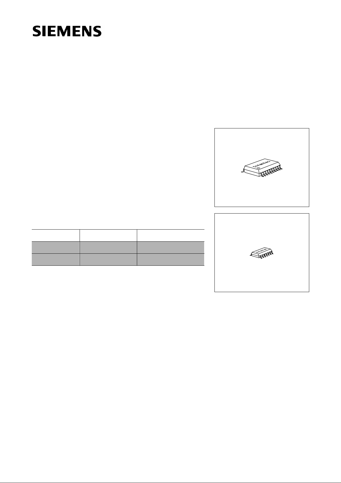
P-DSO-20-6
Type Ordering Code Package
TLE 4262 G Q67006-A9068 P-DSO-20-6 (SMD)
TLE 4262 GM Q67006-A9356 P-DSO-14-4 (SMD)
▼
▼ New type
P-DSO-14-4
Functional Description
TLE 4262 G is a 5-V low-dr op voltage regulator in a P-DSO-20 -6 SMD package. The
maximum input voltage is 45 V. The maximum output current is more than 200 mA. The
IC is short-circuit proof and incorporates temperature protectio n that disables the IC at
overtemperature.
V
The IC regulates an input voltag e
in the range of 6 V < VI < 45 V to V
I
reset signal is generated for an output voltage of
V
< 4.5 V. This voltage threshold can
Q
= 5.0 V. A
Qrated
be decreased to 3.5 V by external connection. The reset delay can be set externally with
a capacitor. The IC can b e switched off via the inhi bit input, which causes th e current
consumption to drop from 720 µA to < 50 µA.
Semiconductor Group 1 1998-11-01
Page 2
TLE 4262
Dimensioning Information on External Components
C
The input capacitor
approx. 1 Ω in series with
capacitance can be dam ped. The output capacitor is necess ary for the stability of the
regulating circuit. Stability is guaranteed at values ≥ 22 µF and an ESR of ≤ 3 Ω wi thin
the operating temperature ran ge. For sm all tole rances o f the rese t delay, the spread of
the capacitance of the dalay capacitor and its temperature coefficient should be noted.
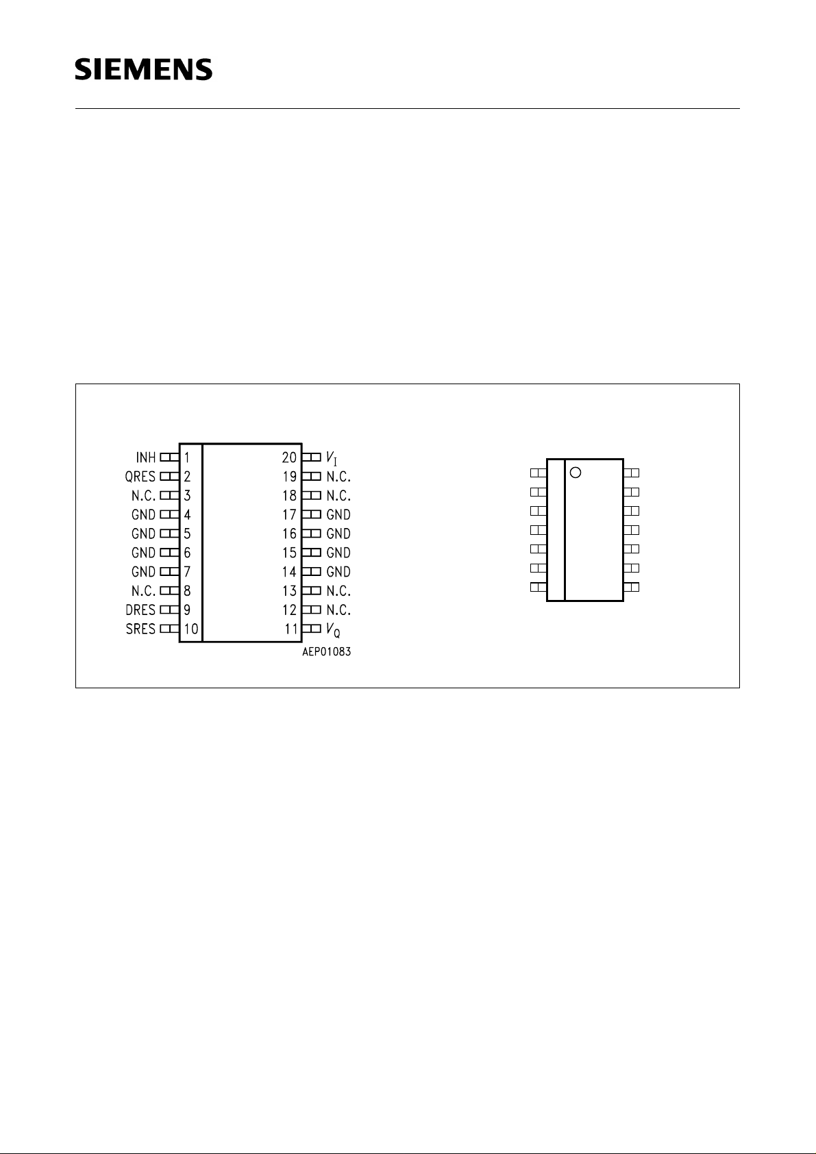
Pin Configuration
(top view)
is necessary for compensating line influences. Using a resistor of
I
C
, the oscillating circuit consisting of input inductivity and input
I
TLE 4262 G
INH
QRES
GND
GND
GND
DRES
SRES
TLE 4262 GM
1
2
3
4
5
6
7
14
13
12
11
10
9
8
AEP02588
V
Ι
N.C.
GND
GND
GND
N.C.
V
Q
Semiconductor Group 2 1998-11-01
Page 3
TLE 4262
Pin Definitions and Functions
Pin Symbol Function
1INHInhibit; TTL-compatible, low-active input
2QRESReset output; open-collector output internally connected to
the output via a resistor of 30 kΩ.
4-7, 14-17 GND Ground
9DRESReset delay; connected to ground by a capacitor
10 SRES Reset threshold; for setting the switching threshold connect
by a voltage divider from output to ground. If this input is
connected to GND, reset is triggered at an output voltage of
4.5 V.
11
20
3, 8, 12,
13, 18, 19
V
V
Q
I
5-V output voltage; block to ground by a 22−µF capacitor.
Input voltage; block to ground directly at the IC by a ceramic
capacitor.
N.C. Not connected
Semiconductor Group 3 1998-11-01
Page 4
TLE 4262
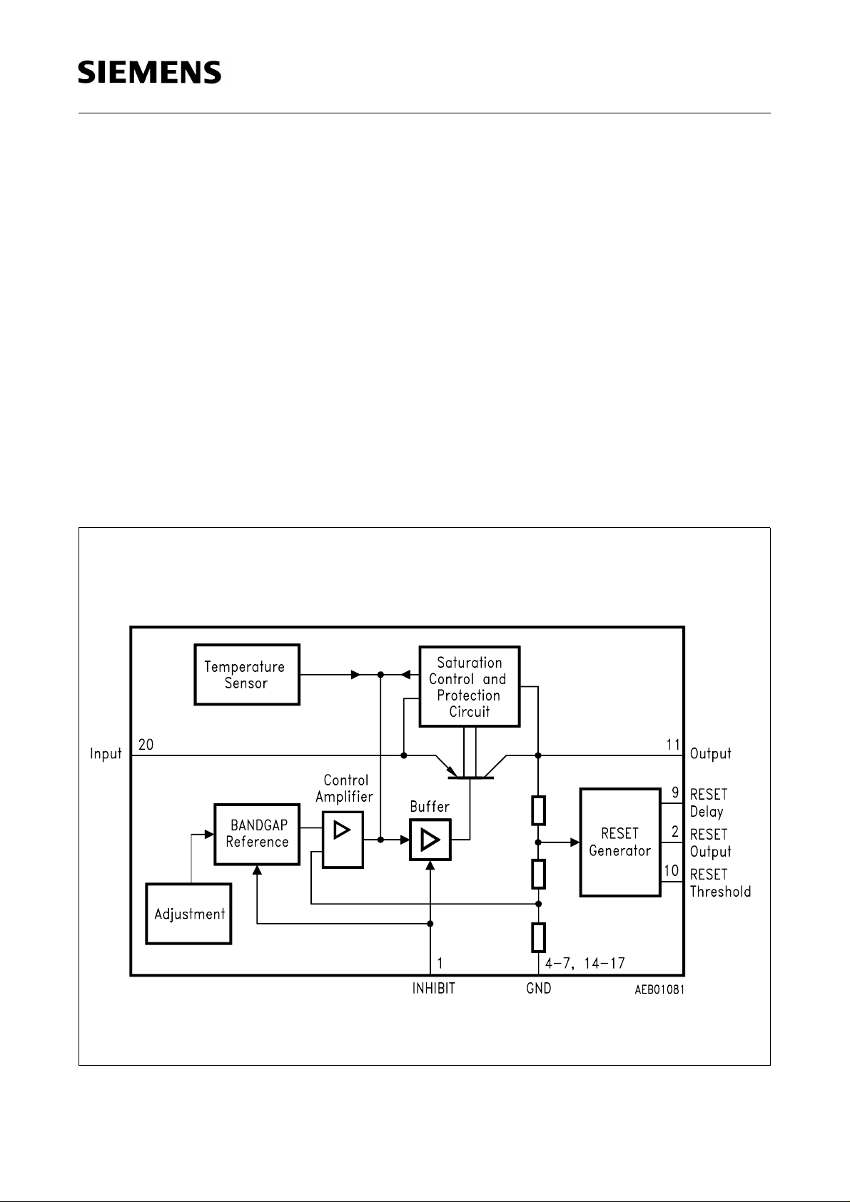
Circuit Description
The control amplifier compares a reference voltage, which is kept highly accurate by
resistance adjustment, to a volt age that is proportion al to the output voltag e and drives
the base of the series transistor via a buffer. Saturation control as a function of the load
current prevents any over-saturation of the power element. If the externally scaled down
output voltage at the reset threshold inp ut drops below 1.3 5 V, the external reset delay
capacitor is discharged by the reset generator. If the voltage on the capaci tor reaches
V
the lower threshold
again until the upper threshold
to GND, reset is triggered at an output voltag e of 4.5 V. The IC can be switched at the
TTL-compatible, low-active inhibit input. It also incorporates a number of internal circuits
for protection against:
● Overload
● Overtemperature
● Reverse polarity
, a reset signal is issued on the reset output and not cancelled
ST
V
is exceeded. If the reset threshold input is connected
dT
Block Diagram
Semiconductor Group 4 1998-11-01
Page 5
TLE 4262
Absolute Maximum Ratings
Parameter Symbol Limit Values Unit Remarks
min. max.
Input
Input voltage
Input current
Reset Output
Voltage
Current
Reset Input
Reset threshold
Reset Delay
Voltage
Current
V
I
V
I
V
V
I
I
I
R
R
RE
d
d
–42
–
– 0.3
–
– 0.3 6 V –
–0.3
–
45
–
42
–
42
–
V
–
V
–
V
–
–
internally limited
–
internally limited
–
internally limited
Output
Voltage
Current
V
I
Q
Q
–5.25
–
V
–
I
V
–
–
internally limited
Inhibit
Voltage
V
e
–42 45 V –
Ground
Current
Semiconductor Group 5 1998-11-01
I
GND
–0.5 – A –
Page 6

TLE 4262
Absolute Maximum Ratings (cont’d)
Parameter Symbol Limit Values Unit Remarks
min. max.
Temperature
Junction temperature
Storage temperature
T
j
T
stg
–
–50
150
150
°C
°C
–
–
Operating Range
Input voltage
Junction temperature T
V
I
j
5.2 45 V
– 40 150 °C–
*)
Thermal resistance
junction-ambient
junction-case
*)
Corresponds with characteristics of drop voltage, output current and power
R
R
th JA
th JC
–
–
70
25
K/W
K/W
soldered
–
description (see diagrams).
Semiconductor Group 6 1998-11-01
Page 7

TLE 4262
Characteristics
V
= 13.5 V; Tj = 25 °C; Ve > 3.5 V; (unless specified otherwise)
I
Parameter Symbol Limit Values Unit Test Condition
min. typ. max.
Normal Operation
Output voltage
Output voltage
Output current limiting
Current consumption;
I
= Ii – I
q
Q
Drop voltage
V
V
I
I
I
I
I
V
Q
q
q
q
q
Load regulation ∆V
Supply-voltage
∆
regulation
V
Q
Q
Dr
4.9 5.00 5.10 V 5 mA ≤ IQ ≤ 150 mA;
V
6 V ≤
– 40 °C ≤
≤ 28 V;
I
T
≤ 125 °C
j
4.95 5.00 5.05 V 6 V ≤ VI ≤ 32 V;
I
= 100 mA
Q
T
> 100 °C
j
200 250 mA –
–
–
–
–
– 0.35 0.6 V IQ = 150 mA
Q
Q
––25mVIQ = 5 mA to 150 mA
– 1525mVVI = 6 V to 28 V;
–
720
10
15
50
–
15
20
µA
µA
mA
mA
V
< 0.8 V
e
I
= 0 mA
Q
I
= 150 mA
Q
I
= 150 mA; Vi = 4.5 V
Q
*)
I
= 150 mA
Q
Ripple rejection
SVR
–54–dBfr = 100 Hz;
V
= 0.5 Vpp
r
Reset Generator
Switching threshold
Switching voltage
Saturation voltage
*)
Drop voltage V
Note: The reset output is low within the range VQ = 1 V to VRT.
Semiconductor Group 7 1998-11-01
≥ 4.5 V; drop voltage = V
I
V
V
V
RT
RE
R
4.2 4.5 4.8 V VRE = 0 V
1.28 1.35 1.42 V VQ > 3.5 V
– 0.10 0.40 V IR = 1 mA
– VQ (below regulating range)
I
Page 8

TLE 4262
Characteristics (cont’d)
V
= 13.5 V; Tj = 25 °C; Ve > 3.5 V; (unless specified otherwise)
I
Parameter Symbol Limit Values Unit Test Condition
min. typ. max.
Saturation voltage V
Charge current I
Delay switching
V
threshold
Switching threshold
Delay time
Delay time
V
t
t
Inhibit
Switch-ON voltage
Switch-OFF voltage
Input current
V
V
I
C
d
dT
ST
D
t
e ON
e OFF
e
– 50 100 mV VQ < V
RT
71014µA–
1.5 1.7 2.1 V –
0.2 0.35 0.55 V –
–17–msCd = 100 nF
–2–µs Cd = 100 nF
3.5 – – V IC turned on
– – 0.8 V IC turned off
51015µA Ve = 5 V
Note: The reset output is low within the range VQ = 1 V to VRT.
Semiconductor Group 8 1998-11-01
Page 9

TLE 4262
Input
6 V...45 V
KL15
Reset
to MC
Application Circuit
Ι
Ι
470 nF
20
11
1
TLE 4262G
2
4
20
9
10
11
22 F 100 kΩ
µ
nF100
Ι
Q
Output
Ωk56
AES01084
µ
22 F
5.6 k
Ω
V
Q
V
R
V
+
Ι
1000 F
V
r
µ
470 nF
TLE 4262G
Ι
e
1
9 4
Ι
d
V
Ι
V
e
C
d
Ι
GND
10
V
cd
Ι
R
2
100 nF
VV
V
Dr
SVR = 20 log
*) Below Regulating Range
-
=
*)
Ι
Q
V
r
V
∆
Q
AES01082
Test Circuit
Semiconductor Group 9 1998-11-01
Page 10

TLE 4262
V
Ι
t
<
t
V
RT
V
Q
d
Ι
V
d
=
d
t
C
V
dT
V
cd
V
ST
t
d
t
t
d
V
R
Power-on-Reset Over-
temperature
Time Response
Voltage Drop
at Input
Undervoltage Secondary
Spike
Load
Bounce
AET01085
Semiconductor Group 10 1998-11-01
Page 11

TLE 4262 G
Charge Current versus
Temperat ure
16
µ
A
Ι
d
14
12
10
8
6
4
2
0
-40
Ι
d
V
Ι
V
cd
= 13.5 V
= 1.5 V
80400
AED01086
120
C
T
j
160
Switching Voltage
V
versus Temperature
3.2
V
V
2.8
V
Ι
2.4
VV
40
dT
V
ST
2.0
1.6
1.2
0.8
0.4
0
0-40
and VST
dT
AED01087
= 13.5 V
,
cd
12080
T
j
C
160
Reset Switching Threshold
versus Temperature
1.6
V
V
RE
1.4
1.2
1.0
0.8
0.6
0.4
0.2
0
-40
40
0 160
80 120
AED01088
C
T
j
Current Consumption of Inhibit
versus Temperature
Output Current
12
µ
A
Ι
e
10
8
V
e
6
4
2
0
-40 0 8040 120
= 5 V
AED01089
C
T
j
160
Semiconductor Group 11 1998-11-01
Page 12

TLE 4262 G
Output Voltage versus
Temperat ure
5.2
V
V
Q
5.1
5.0
V
e
4.9
4.8
4.7
4.6
0-40
40
= 13.5 V
12080
AED01090
160
C
T
j
Output Current versus
Input Voltage
300
mA
T
Ι
Q
250
200
150
100
50
0
= 25 C
j
100
20
30
AED01091
40
50
V
V
Ι
Input Response
2
V
∆
V
Ι
1
0
40
mV
V
∆
Q
20
0
-20
-40
-10
t
=
r
_
~
t
f
C
= 22 F
Q
µ
1 s
20100
µ
30
AED01092
40
50
s
µ
t
Load Response
295
mA
Ι
∆
Q
150
5
200
mV
∆
V
Q
100
0
-100
-200
010-10
C
= 22 F
Q
20
µ
30
AED01093
40
50
µ
s
t
Semiconductor Group 12 1998-11-01
Page 13

TLE 4262
Drop Voltage versus
Output Current
800
mV
V
Dr
700
600
500
T
= 125 C
400
300
200
100
0
j
25 C
500 100
200150
AED01094
300
mA
Ι
Q
Current Consumption versus
Output Current
200
AED01095
mA
Ι
32
mA
Ι
q
28
24
20
V
= 13.5 V
Ι
16
12
8
4
0
100050
150
300
Q
Current Consumption versus
Input Voltage
30
AED01096
40
V
30
mA
Ι
q
25
20
R
15
10
5
0
L
20010
= 25
Ω
Output Voltage versus
Input Voltage
12
V
V
Q
10
8
6
R
= 25
L
4
2
50
V
Ι
0
0
4
2
AED01097
Ω
68
10
V
V
Ι
Semiconductor Group 13 1998-11-01
Page 14

Package Outlines
P-DSO-20-6
(Plastic Dual Small Outline)
1.27
+0.15
0.35
2)
0.2 24x
1120
-0.1
0.2
-0.2
2.45
0.1
7.6
2.65 max
10.3
0.35 x 45˚
1)
-0.2
+0.8
0.4
±0.3
+0.09
0.23
TLE 4262
8˚ max
Weight approx. 0.6 g
GPS05094
110
12.8
-0.2
1)
Index Marking
1) Does not include plastic or metal protrusions of 0.15 max per side
2) Does not include dambar protrusion of 0.05 max per side
Sorts of Packing
Package outlines for tubes, trays etc. are contained in our
Data Book “Package Information”.
SMD = Surface Mounted Device
Dimensions in mm
Semiconductor Group 14 1998-11-01
Page 15

P-DSO-14-4
(Plastic Dual Small Outline)
-0.1
0.2
-0.2
1.45
4
-0.2
1.75 max
TLE 4262
0.35 x 45˚
1)
+0.06
0.19
0.35
1.27
+0.15
2)
0.1
0.2 14x
±0.2
6
0.4
+0.8
8˚ max.
14 8
17
1)
8.75
-0.2
Index Marking
1) Does not include plastic or metal protrusion of 0.15 max. per side
2) Does not include dambar protrusion of 0.05 max. per side
GPS05093
Sorts of Packing
Package outlines for tubes, trays etc. are contained in our
Data Book “Package Information”.
SMD = Surface Mounted Device
Dimensions in mm
Semiconductor Group 15 1998-11-01
 Loading...