

Page 1
TLE 4261
5-V Low-Drop Voltage Regulator
Features
● Very low-drop voltage
● Very low quiescent current
● Low starting-current consumption
● Proof against reverse polarity
● Input voltage up to 42 V
● Overvoltage protection up to 65 V (≤ 400 ms)
● Short-circuit proof
● External setting of reset delay
● Integrated watchdog circuit
● Wide temperature range
● Overtemperature protection
● Suitable for automotive use
● EMC proofed (100 V/m)
TLE 4261
Bipolar IC
P-TO220-7-1
P-TO220-7-2
Type Ordering Code Package
TLE 4261 Q67000-A9003 P-TO220-7-1
▼
TLE 4261 S Q67000-A9109 P-TO220-7-2
▼
TLE 4261 G Q67000-A9059 P-DSO-20-6 (SMD)
▼
Please also refer to the new pin compatible
▼
device TLE 4271
P-DSO-20-6
Functional Description
TLE 4261 is a 5-V low-drop volta ge regulator in a P-TO220-7 or i n a P-DSO package.
The maximum input voltage is 42 V (65 V/≤ 400 ms). The device can produce an output
current of more than 500 mA. It is short-circuit proof and incorporates temperature
protection that disables the circuit at impermissibly high temperatures.
Semiconductor Group 1 1998-11-01
Page 2

TLE 4261
Application Description
V
The IC regulates an input voltage
reset signa l is generat ed for a maxim um output voltage of
in the range VI = 6 V to 40 V to V
I
V
less than 4.75 V. The reset
Q
delay can be set ext ernally with a capacitor. A con nected micr oprocessor is moni tored
by the integrated watchdog c ircu it. Connecting this input to the input vol tage make s the
watchdog function inactive. The presence of a voltage less than 2 V on inhibit input
disables the regulator. The current consumption drops to max. 50 µA.
Design Notes for External Components
C
The input capacitor
causes a low-resista nt powerline and limits the rise ti mes of the
I
input voltage. The IC is protected against rise times up to 100 V/µs. It is possible to damp
the tuned circuit consisting of supply inductance and input capacitance with a resistor of
C
approx. 1 Ω in series to
.
I
The output capacitor maintains the stability of the regulating loop. Stability is guaranteed
with a rating of 22 µF at an ESR of 3 Ω max. in the operating temperature range.
= 5.0 V. A
Qrated
Circuit Description
The control amplifier compares a reference voltage, which is kept highly accurate by
resistance adjustment, to a voltage that is proportional to the output voltage and controls
the base of the series PNP transistor via a buffer. Saturation control as a function of the
load current prevents any over-saturation of the power element. If the output voltage
drops below 95.5 % of its typical value for more than 2 µs, a reset signal is triggered on
pin 3 and an external capacitor is discharged on pin 5. The reset signal is not cancelled
V
until the voltage on the capacito r has exceeded the upper switchi ng threshold
DT
. A
positive-edge-triggered watchdog circuit monitors the connected microprocessor and
will likewise trigger a reset if puls es are missing . The IC can be disa bled by a low le vel
on the inhibit input and the current consumption drops to < 50 µA.
The IC also incorporates a number of circuits for protection against:
● Overload
● Overvoltage
● Overtemperature
● Reverse polarity
Semiconductor Group 2 1998-11-01
Page 3
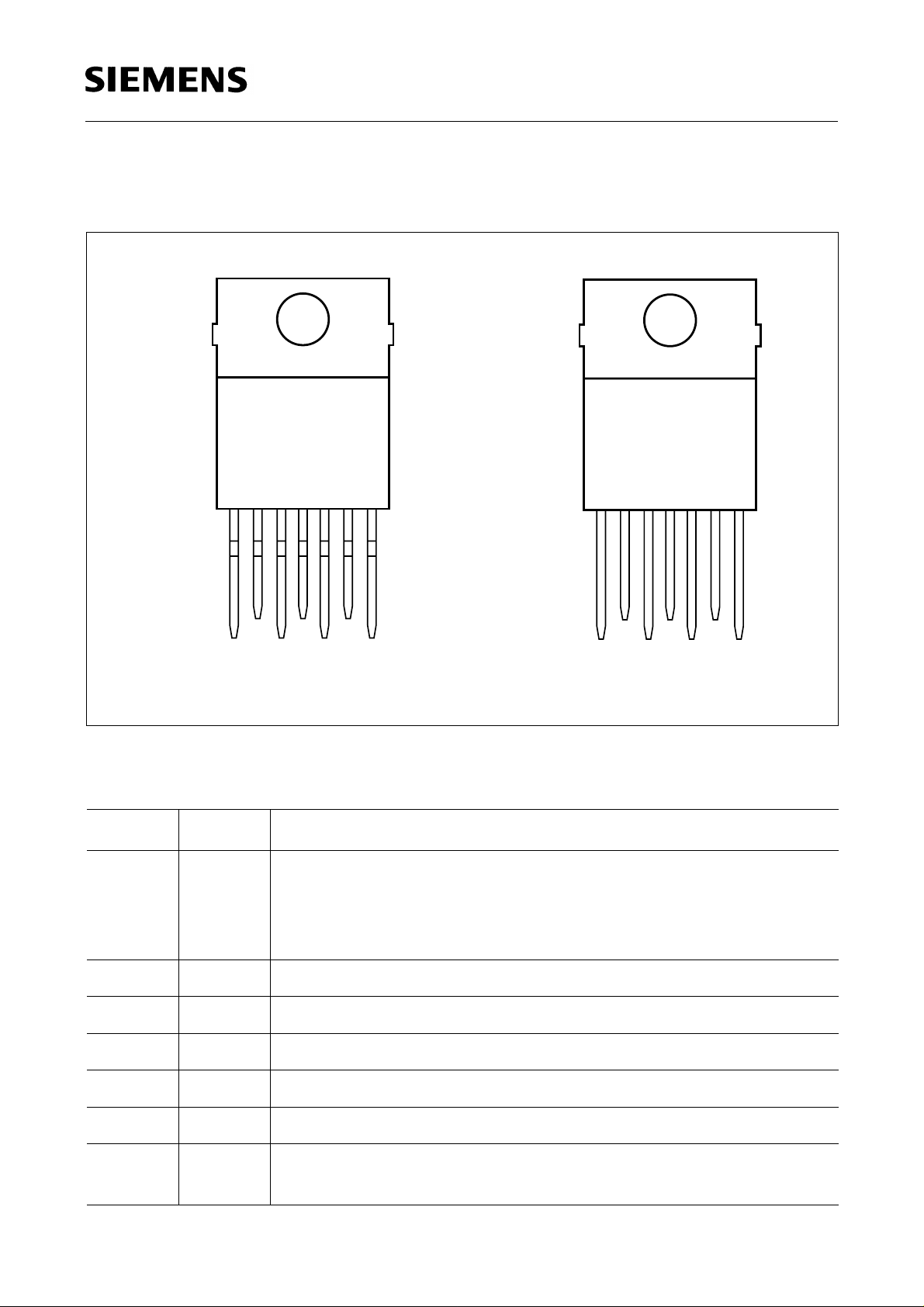
Pin Configuration
(top view)
TLE 4261
TLE 4261
INH
V
QRES
Ι
4321567
GND
Watch
DRES
V
Q
AEP00592
TLE 4261 S
INH
QRES
V
Ι
4321567
GND
Watch
DRES
V
Q
AEP01181
Pin Definitions and Functions (TLE 4261; S)
Pin Symbol Function
1
V
I
Input voltage; block a capacitor directly to ground on the IC. The
capacitor rating will depend on the vehicle electrical system.
Oscillation of the input voltage can be damped by a resistor of
approx. 1 Ω in series with the input capacitor.
2INHInhibit; switches off the IC when low.
3QRESReset output; open-collector output controlled by the rese delay.
4GNDGround
5DRESReset delay; wired to ground using a capacitor.
6WatchWatchdog; monitors the microprocessor when active.
7
V
Q
5-V output voltage; block to ground using a capacitor of ≥ 22 µF.
ESR is ≤ 3 Ω in the operating temperature range.
Semiconductor Group 3 1998-11-01
Page 4
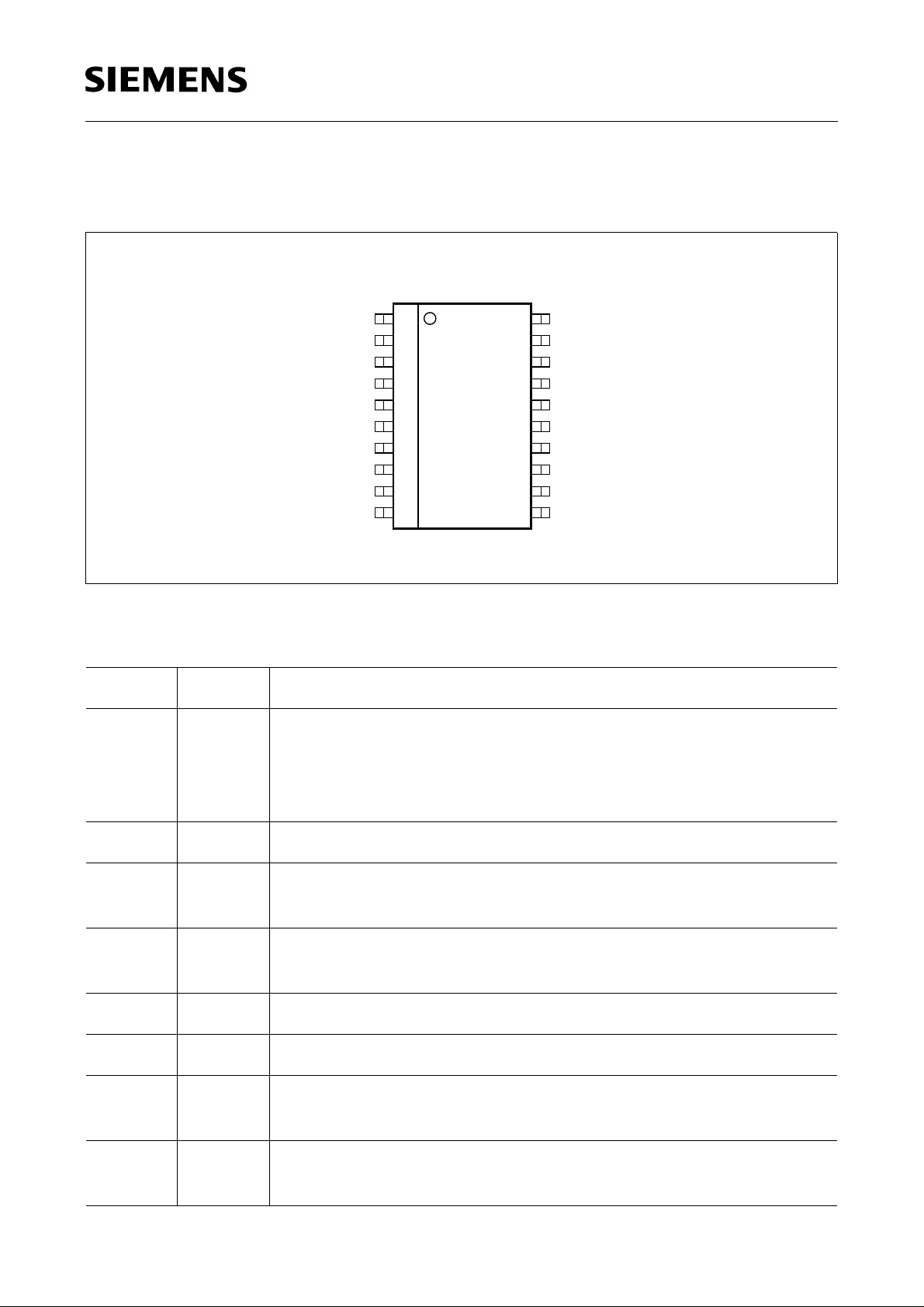
Pin Configuration
(top view)
TLE 4261
TLE 4261 G
N.C.
N.C.
QRES
GND
GND 5
GND
N.C.
DRES
N.C.
1
2
3
4
6
7
8
9
10
AEP01182
Pin Definitions and Functions (TLE 4261 G)
Pin Symbol Function
18
V
I
Input voltage; block a capacitor directly to ground on the IC. The
capacitor rating will depend on the vehicle electrical system.
Oscillation of the input voltage can be damped by a resistor of
approx. 1 Ω in series with the input capacitor.
20
19
18
17
16
15
14
13
12
11
INH
N.C.
V
Ι
GND
GND
GNDGND
GND
N.C.
V
Q
Watch
20 INH Inhibit; switches off the IC when low.
3QRESReset output; open-collector output controlled by the reset
delay.
4 - 7
GND Ground; internally connected with pins 14 to 17.
14 - 17
9 DRES Reset delay; wired to ground using a capacitor.
11 Watch Watchdog; monitors the microprocessor when active.
12
V
Q
5-V output voltage; block to ground using a capacitor of ≥ 22 µF.
ESR is ≤ 3 Ω in the operating temperature range.
1, 2, 8, 10,
N.C. Not connected
13, 19
Semiconductor Group 4 1998-11-01
Page 5
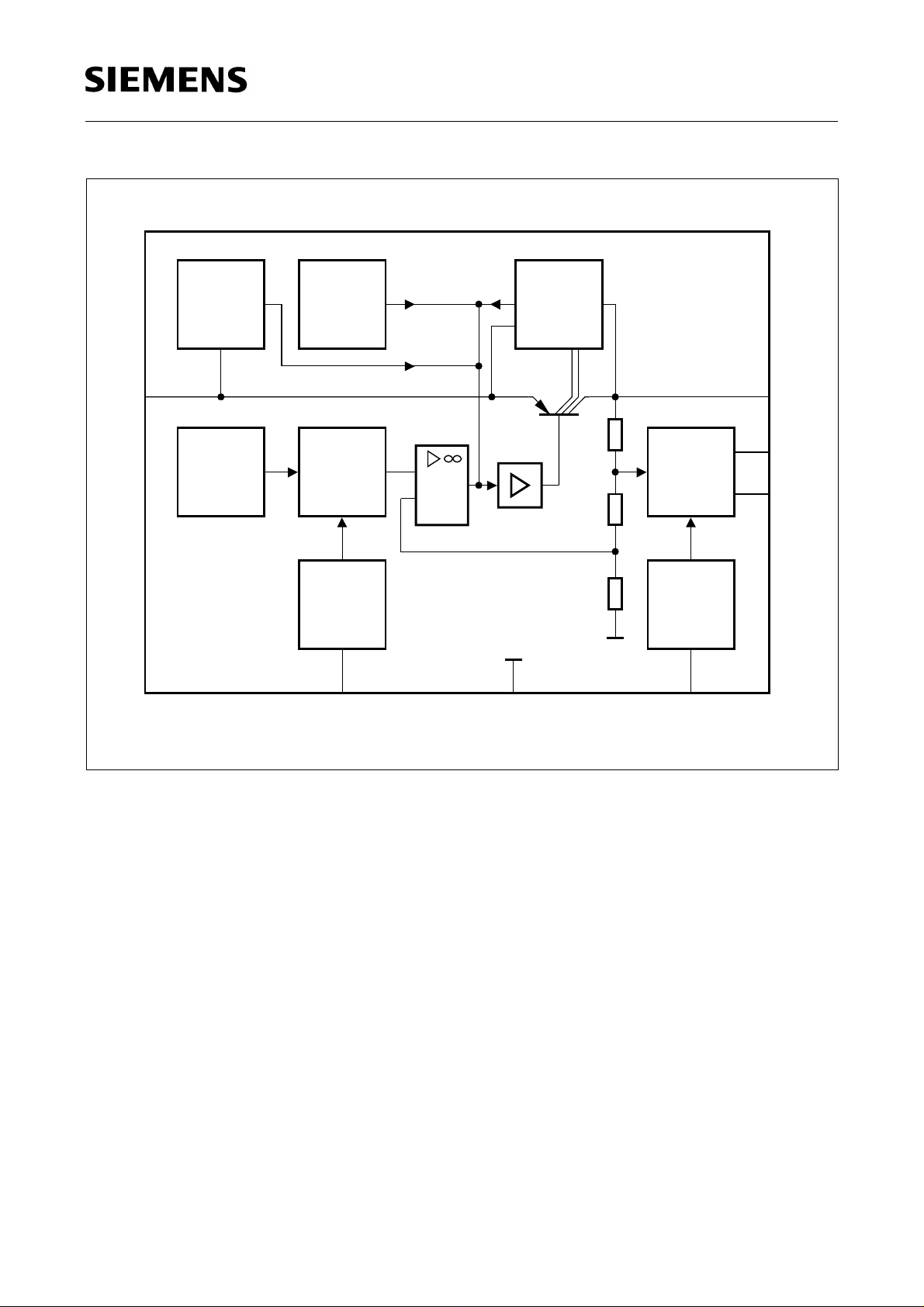
TLE 4261
Overvoltage
Monitoring
1
Input
(18)
Adjustment
Numbers in parentheses f or T LE 4261 G
Temperature
Sensor
BANDGAP
Reference
Inhibit
2(20)
Inhibit GND Watchdog
Control
Amplifier
+
-
(4-7)
Saturation
Control and
Protection
Buffer
RESET
Generator
Watchdog
(11) 64(14-17)
7
(12)
5
(9)
3
(3)
AEB00002
Output
RESET
Delay
RESET
Output
Block Diagram
Semiconductor Group 5 1998-11-01
Page 6
TLE 4261
Absolute Maximum Ratings
T
= – 40 to 150 °C
j
Parameter Symbol Limit Values Unit Remarks
min. max.
Input
Input voltage
Input voltage
Input current
Inhibit
Voltage
Current
Reset Output
Voltage
Current
Ground
Current
Reset Delay
V
V
I
I
V
I
2
V
I
R
I
GND
I
I
–42
–
–
2
–0.3
–
R
– 0.3
–
45
65
1.6
42
5
42
–
V
V
A
V
mA––
V
–
–
t ≤ 400 ms
–
–
limited internally
–0.5A–
Voltage
Current
V
I
D
D
–0.3
–
42
–
V
–
–
limited internally
Watchdog
Voltage
V
W
–0.3 V
I
V–
Output
V
I
– V
I
Q
Differential voltage
Current
Semiconductor Group 6 1998-11-01
Q
–5.25
–
V
I
1.4
V
A
–
–
Page 7

TLE 4261
Absolute Maximum Ratings (con t’d)
T
= – 40 to 150 °C
j
Parameter Symbol Limit Values Unit Remarks
min. max.
Temperature
Junction temperature
Storage temperature
T
T
Operating Range
Input voltage
Junction temperature
V
T
Thermal Resistances
System-air
System-case
1)
Figures in parenthesis refer to TLE 4261 G.
R
R
j
stg
I
j
th SA
th SC
–
–50
150
150
°C
°C
–
–
–32Vsee diagram
– 40 150 °C–
65 (70)
–
3 (15)
1)
1)
K/W
K/W––
Semiconductor Group 7 1998-11-01
Page 8

TLE 4261
Characteristics
V
= 13.5 V; Tj = 25 °C; V2 ≥ 6 V; (unless specified otherwise)
I
Parameter Symbol Limit Values Unit Test Condition
min. typ. max.
Normal Operation
Output voltage
Output voltage
Output current
Output current
Current consumption;
I
= II – I
q
Q
Current consumption;
I
= II – I
q
Q
Current consumption;
I
= II – I
q
Q
V
V
I
I
I
I
I
Q
Q
Q
Q
q
q
q
4.75 5.00 5.25 V 25 mA ≤ IQ ≤ 500 mA;
V
6 V ≤
– 40 °C ≤
≤ 28 V;
I
T
≤ 125 °C
j
4.85 5.00 5.15 V 25 mA ≤ IQ ≤ 150 mA
V
6 V ≤
≤ 40 V
I
––50µA0 V ≤ VI ≤ 2 V; V2 = VI;
T
– 40 °C ≤
≤ 125 °C
j
500 1000 – mA VI = 17 V to 28 V
––3.5mAIQ = 0; VW > 6 V
– 5.0 10 mA 6 V ≤ VI ≤ 28 V
I
= 150 mA
Q
–4065mA6 V ≤ VI ≤ 28 V
I
= 500 mA
Q
Current consumption;
I
= II – I
q
Q
Drop voltage
Drop voltage
Load regulation ∆
Supply voltage
I
V
V
∆
q
Dr
Dr
V
Q
V
Q
regulation
Supply voltage
V
∆
Q
regulation
Semiconductor Group 8 1998-11-01
–4580mAVI < 6 V; IQ ≤ 500 mA;
– 0.35 0.5 V VI = 4.5 V; IQ = 0.5 A
–0.20.3VVI = 4.5 V; IQ = 0.15 A
–1535mV25 mA ≤ IQ ≤ 500 mA
–1550mV6 V ≤ VI ≤ 28 V
I
= 100 mA
Q
– 5 25 mV 6 V ≤ VI ≤ 16 V
I
= 100 mA
Q
Page 9

TLE 4261
Characteristics (cont’d)
V
= 13.5 V; Tj = 25 °C; V2 ≥ 6 V; (unless specified otherwise)
I
Parameter Symbol Limit Values Unit Test Condition
min. typ. max.
Ripple rejection
Temperature drift of
output vol tage
Inhibit Operation
Current consumption
Current consumption
Switching threshold
for inhibit
Switching threshold
for inhibit
Reset Generator
SVR
α
VQ
I
1
I
2
V
2
V
2
–54–dBfr = 100 Hz;
V
= 0.5 Vpp
r
–2 ×
10
–1/°C– 40 °C ≤ Tj ≤ 150 °C
–4
––50µA V2 < 2 V; IQ = 0
––100µA V2 = 6 V
5.0 5.5 6.0 V IC turned ON
2.0 2.7 3.7 V IC turned OFF
Switching threshold
Saturation voltage,
V
V
RT
R
94 95.5 97 % in % of V
I
> 500 mA; VI = 6 V
Q
– 0.250.40V IR = 1 mA
Q
reset output
Reverse current
Charge current
Switching threshold
Delay switching
I
I
V
V
R
d
ST
DT
––1µA VR = 5 V
18.75 25 31.25 µA VC = 1.5 V
0.9 1 1.1 V –
2.25 2.50 2.75 V –
threshold
Saturation voltage,
V
C
––100mVVI = 4.5 V and I
d
delay output
Semiconductor Group 9 1998-11-01
Page 10

TLE 4261
Characteristics (cont’d)
V
= 13.5 V; Tj = 25 °C; V2 ≥ 6 V; (unless specified otherwise)
I
Parameter Symbol Limit Values Unit Test Condition
min. typ. max.
Delay time t
Delay time
Watchdog
Turn-OFF voltage
Discharge current
Switching voltage
Pulse interval
General Data
Turn-OFF voltage
Turn-OFF hysteresis ∆
t
V
I
V
T
V
D
t
W
CD
CD
W
IOFF
V
–10–msCD = 100 nF
–2–µs–
5.2 5.6 6.0 V –
5.6 7.5 9.4 µA VC = 1.5 V
2.95 3.05 3.15 V –
–35–msCD = 100 nF
41 43 45 V IQ < 1 mA
I
–6.5–V–
Leakage current
Reverse output
I
QS
I
QR
current
Semiconductor Group 10 1998-11-01
––50µA VQ = 0 V; VI = 45 V
––1.5mAVQ = 5 V; VI and V2
open
Page 11

TLE 4261
Input
6 V to 40 V
470
nF
KL15 7 V to 18 V
Application Circuit
17
2
TLE 4261
6
4
5
3
100 nF
22 µF
k4.7 Ω
100 k
Output
Ω
RESET
From Cµ
AES00021
V
+
V
Ι
VV
=
Dr
= 20 log
SVR
Test Circuit
R
-
Ι
1000 Fµ
V
Q
Ι
Ι
17
470 nF
TLE 4261
Ι
3
2
54
Ι
V
2
V
C
D
C
Ι
GND
D
ΙQΙ
/
SC
22 Fµ
4.7 kΩ
V
Q
Ι
R
3
6
V
W
V
R
100 nF
AES00135
V
R
V
∆
Q
Semiconductor Group 11 1998-11-01
Page 12

TLE 4261
V
-----------------------------------------------------------
t
W
–()I
CD
V
ST
I
×
DICD
+()
CDID
C
;
D tdw
V
DT
--------------------------------
=
Time Response in Watchdog Condition
> 6 V
V
Wmin
V
W
ΙVOFF
V
Ι
V
RT
V
Q
V
DT
V
V
C
ST
V
R
∆
V
Ι
∆
V
RT
Ι
d
V
D
=
d
tC
D
V
–()
ST
C
I
D
D
3.3 V
t
D
<
V
OFFΙ
t
<
t
Overvoltage
Spike
Over-
voltage
Over-
temperature
Undervoltage Secondary
Spike
Shortcircuit
on Output
AET00593
Timing with Watchdog OFF
Semiconductor Group 12 1998-11-01
Page 13

TLE 4261
Drop Voltage versus
Output Current
800
mV
Dr
700
= 4.5 V
V
Ι
600
500
400
300
200
100
0
0V100 200 300 600
T
j
T
j
= 125
= 25
Current Consumption versus
Output Current
AED00586
80
mA
q
70
= 13.5 V
V
Ι
60
50
C
40
30
20
C
10
0
400
mA
0Ι100 200 300 600
400
AED00588
mA
Current Consumption versus
Input Voltage
120
Ι
q
mA
100
R
=10 Ω
L
80
60
40
20
Ι
Q
AED00026
Output Voltage versus
Input Voltage
12
V
Q
V
10
R
=10 Ω
L
8
6
4
2
Ι
Q
AED00027
0
0
10 20 30 50
40
V
V
Ι
0
0
24
610
8
V
V
Ι
Semiconductor Group 13 1998-11-01
Page 14

TLE 4261
Output Voltage versus
Temperat ure
5.20
V
Q
V
5.10
V
=
13.5 V
Ι
5.00
4.90
4.80
4.70
4.60
-40
0 40 80 160
AED00028
120
Output Current versus
Input Voltage
1.2
Ι
Q
mA
1.0
= 25
T
C
j
0.8
0.6
0.4
0.2
C
j
0
0
10 20 30 50
AED00594
40
V
V
Ι
Input Step Response
2
∆
V
Ι
1
0
40
V
∆
Q
mV
20
0
-20
-40
-10V01020 50
tt
RF
=C22 µs
Q
30
AED00595
_
~
1=
µs
sµ
t
Load Step Response
mA
∆
Q
500
25
200
V
∆
mV
Q
100
0
-100
-200
-10Ι01020 50
Q
=C22 µs
30
AED00596
sµ
t
Semiconductor Group 14 1998-11-01
Page 15

TLE 4261
Charge Current ID and Discharge
I
Current
40
µA
Ι
35
30
25
20
15
10
5
0
versus Temperature
CD
AED01322
V
= 13.5 V
Ι
V
= 1.5 V
C
Ι
d
Ι
Cd
40-40 0
T
j
C
16080 120
Switching Voltage
V
versus Temperature
ST
4
V
V
3
2
1
0
-40
V
CD
V
= 13.5 V
Ι
80040
and
V
Cd
V
ST
AED01323
120 160
C
T
j
Pulse Interval
Temperat ure
1.6
ms
T
W
1.4
1.2
1.0
0.8
0.6
0.4
0.2
0
0-40 40
T
versus
W
= 13.5 V
V
Ι
= 100 nF
C
d
AED01324
12080 160
C
T
j
Current Consumption of Inhibit at the
Switching Point vers us Temperat ure
120
µ
A
Ι
20
100
80
60
40
20
0
40-40 0
80 120
AED01325
ON
OFF
160
C
T
j
Semiconductor Group 15 1998-11-01
Page 16

Package Outlines
P-TO220-7-1
(Plastic Transistor Single Outline)
TLE 4261
+0.4
10
10.2
-0.2
+0.1
3.75
2.8
17
1.27
1)
+0.1
0.6
0.6
1) 0.75
1) 0.75
at dam bar (max 1.8 from body)
-0.15
im Dichtstegbereich (max 1.8 vom Körper)
-0.15
7x
M
+0.1
1.27
±0.4
19.5 max
16
2.6
0.4
±0.4
4.5
4.6
-0.2
+0.1
8.4
1 x 45˚
-0.2
8.8
±0.4
±0.3
15.4
±0.3
±0.3
8.6
10.2
GPT05108
Weight approx. 2.1 g
Sorts of Packing
Package outlines for tubes, trays etc. are contained in our
Data Book “Package Information”.
Dimensions in mm
Semiconductor Group 16 1998-11-01
Page 17

Package Outlines (cont’d)
P-TO220-7-2
(Plastic Transistor Single Outline)
+0.4
10
10.2
-0.2
+0.1
3.75
2.8
1.27
+0.1
4.6
-0.2
1 x 45˚
-0.2
8.8
TLE 4261
15.4
Weight approx. 2.1 g
17
11
1.27
+0.1
0.6
1) 0.75
1) 0.75
at dam bar (max 1.8 from body)
-0.15
im Dichtstegbereich (max 1.8 vom Körper)
-0.15
13
+0.1
0.4
1)
M
0.6
2.6
7x
GPT05257
Sorts of Packing
Package outlines for tubes, trays etc. are contained in our
Data Book “Package Information”.
Dimensions in mm
Semiconductor Group 17 1998-11-01
Page 18

Package Outlines (cont’d)
P-DSO-20-6
(Plastic Dual Small Outline)
1.27
+0.15
0.35
2)
0.2 24x
1120
-0.1
0.2
-0.2
2.45
0.1
7.6
2.65 max
10.3
0.35 x 45˚
1)
-0.2
+0.8
0.4
±0.3
+0.09
0.23
TLE 4261
8˚ max
Weight approx. 0.6 g
GPS05094
110
12.8
-0.2
1)
Index Marking
1) Does not include plastic or metal protrusions of 0.15 max per side
2) Does not include dambar protrusion of 0.05 max per side
Sorts of Packing
Package outlines for tubes, trays etc. are contained in our
Data Book “Package Information”.
SMD = Surface Mounted Device
Dimensions in mm
Semiconductor Group 18 1998-11-01
 Loading...