

Page 1
Intelligent Sixfold Low-Side Switch
Features
● Double low-side switch, 2 x 0.5 A
● Quad low-side switch, 4 x 50 mA
● Power limitation
● Open-collector outputs
● Overtemperature shutdown
● Status monitoring
● Shorted-load protection
● Integrated clamp Z-Diodes
● Temperature range – 40 to 110 °C
TLE 4216 G
Bipolar IC
P-DSO-24-3
Type Ordering Code Package
TLE 4216 G Q67000-A9108 P-DSO-24-3 (SMD)
TLE 4216 G is an integrated, sixfold low-side power switch with power limiting of the
0.5 A outputs, shorted load protection of the 50 mA switches and Z-diodes on all
switches from output to ground. TLE 4216 G is particularly suitable for automotive and
industrial applications.
Semiconductor Group 1 08.96
Page 2
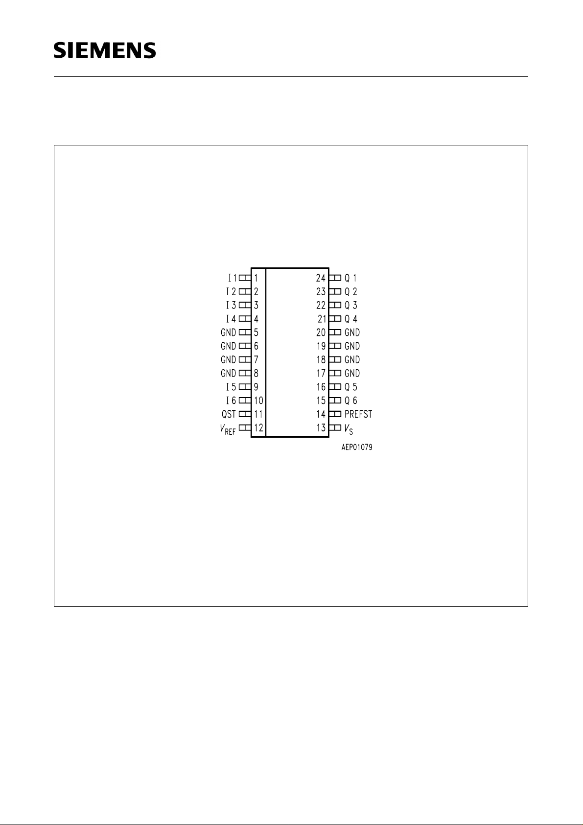
Pin Configuration
(top view)
TLE 4216 G
TLE 4216 G
Semiconductor Group 2
Page 3
Pin Definitions and Functions
TLE 4216 G Symbol Function
Pin No.
1, 2, 3, 4 I1, I2, I3, I4 Inputs of 50-mA switches 1, 2, 3, 4
5, 6, 7, 8 GND Ground, cooling
9, 10 I5, I6 Inputs of 0.5 A switches 5, 6
TLE 4216 G
11 Q
12
V
ST
REF
Status analog output
Reference voltage; a higher reference voltage than
the internal one can be applied from the exterior as
a voltage reference for the status output (A/D
converter).
13
V
S
Supply voltage
14 PREFST Preferred state (low = preferred state of all outputs
regardless of inputs)
15, 16 Q6, Q5 Outputs 6, 5 (0.5 A), open collector
17, 18, 19, 20 GND Ground, cooling
21, 22, 23, 24 Q4, Q3,
Outputs 4, 3, 2, 1 (50 mA), open collector
Q2, Q1
Semiconductor Group 3
Page 4
TLE 4216 G
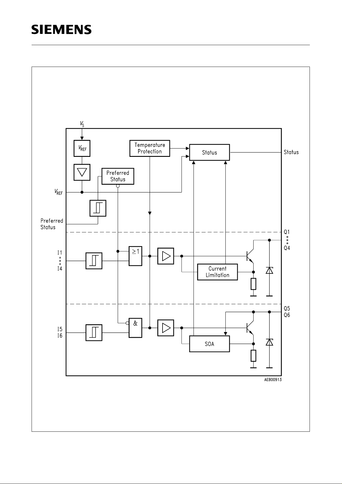
Block Diagram
Semiconductor Group 4
Page 5
TLE 4216 G
Circuit Description
Input Circuits
The control inputs and the preferred-state input consist of TTL-compatible Schmitt
triggers with hysteresis. Driven by these stages the buffer amplifiers convert the logic
signal necessary for driving the NPN power transistors.
Switching Stages
The output stages consist of NPN power transistors with open collectors. Each stage has
its own protective circuit for limiting power dissipation and shorted-load current, which
makes the outputs shorted-load protected to the supply voltage throughout the operating
range. Integrated Z-diodes limit positive voltage spikes that occur when inductive loads
are discharged.
Monitoring and Protective Functions
Each output is monitored in its activated status for overload. Furthermore, large parts of
the circuitry are shutdown (control, output stages). The information from these
malfunctions is ORed and applied to the status output. If several malfunctions appear
simultaneously, the highest voltage level will dominate. The IC is also protected against
thermal overload. If a chip temperature of typically 160 °C is reached, overtemperature
is signalled on the status output. If the temperature continues to increase, all outputs are
turned off at 170 °C.
If the minimum supply voltage for functioning is not maintained, the output stages
become inactive. At a supply voltage of 2 to 4 V, the outputs are switched to a preferred
state regardless of the level on pin PREFST. If the preferred state is to be maintained
beyond this range, pin PREFST must be switched to low potential. Above a supply
voltage of typical 3 V (max. 4 V) the preferred state is controlled by pin PREFST. From
4 to 5.2 V the logic operation of the outputs is guaranteed, but the status output cannot
be evaluated. At a supply voltage of 5.2 to 30 V the full function is guaranteed.
Semiconductor Group 5
Page 6

TLE 4216 G
Application Description
Applications in automotive electronics require intelligent power switches activated by
logic signals, which are shorted-load protected and provide error feedback.
The IC contains six power switches connected to ground (low-side switch). On inductive
loads the integrated Z-diodes clamp the discharging voltage.
By means of TTL signals on the control inputs (active high) all six switches can be
activated independently of another when a high level appears on the preferred-state
input. When there is a low level on the preferred-state input, switches 1 to 4 are switched
on, switches 5 and 6 are switched off regardless of the input level. The inputs are highly
resistive and therefore must not be left unconnected, but should always be on fixed
potential (noise immunity).
The status output signals the following malfunctions by analog voltage levels:
● Overload
● Overtemperature
Possible Input and Output Levels
Supply Voltage
2 to 4 V
4 to 30 V
4 to 30 V
V
PREFST I1 … I6 Q1 … Q4 Q5, Q6
S
L
H
H
X
L
H
L
H
L
H
H
L
Semiconductor Group 6
Page 7

TLE 4216 G
Absolute Maximum Ratings
T
= − 40 to 150 °C
j
Parameter Symbol Limit Values Unit Remarks
min. max.
Voltages
Supply voltage
Supply voltage,
V
V
S
Q1-6
load circuit
Input voltage
Input voltage
V
I1-6
V
PREFST
V
REF ext
Currents
Switching current IQ1-I
Current on reverse
I
Q5, Q6
poling in load circuit
Current on reverse
I
Q1-Q4
poling in load circuit
,
Q6
– 1 40 V
– 0.7 25 V
0 V
S
V
– 0.7 7 V
– 0.5 A
–50 mA
limited internally
Output current
I
Z5-Z6
positive clamp
Output current
I
Z1-Z4
positive clamp
Junction temperature
Storage temperature
T
j
T
stg
– 40 150 °C Thermal overload
– 50 150 °C
Semiconductor Group 7
0.7 A
70 mA
shutdown at 170 °C
Page 8

TLE 4216 G
Operating Range
Parameter Symbol Limit Values Unit Remarks
min. max.
Supply voltage
Supply voltage in
load circuit
Ambient temperature
Supply voltage for load
short-circuit
Input current (high)
Thermal resistance
Junction-ambient
V
V
T
V
I
R
S
Q1-6
A
S
IH
th JA
5.2 30 V V
is guaranteed at
V
status output cannot
be evaluated.
– 0.3 24 V
– 40 110 °C
16 V
100 µA
65 K/W P-DSO-24-3
≤VS, functioning
REF
= 4 – 5.2 V but
S
Semiconductor Group 8
Page 9

TLE 4216 G
Characteristics
V
= 5 to 12 V; Tj = – 25 to 140 °C
S
Parameter Symbol Limit Values Unit Test Condition
min. typ. max.
General
Supply current
Supply current
Quiescent current
I
S
I
S
I
S
Logic (Control inputs + preferred state)
H-switching threshold
L-switching threshold
Hysteresis
V
V
∆V
IH
IL
I
1.3
0.9
0.3
Input current
Input current
L-input current
I
I
– I
IL
–2
0
Switching Stages
Load current
Saturation voltage
Saturation voltage
Saturation voltage
Turn-ON time
Turn-OFF time
I
Q1-Q4
V
QSat 5, 6
V
QSat 1-4
V
QSat 1-4
t
D-ON
t
D-OFF
50
0.2
0.2
50
36
8
1.8
1.2
0.6
0.5
0.4
1
1
70
50
11
2.1
1.5
1.0
2
20
0.8
0.6
0.22
1.5
1.5
mA
mA
mA
V
V
V
µA
µA
mA
V
V
V
µs
µs
V
> VIH; VIP > V
I
V
> VIH; VIP > VIH;
I
V
=5 V
S
V
< VIL; VIP > V
I
0.9 V <
0.5 V <
V
= 2 V
S
V
< 6 V
I
V
< 0.9 V
I
(preferred state)
I
= 0.4 A; VI > V
Q
I
= 50 mA; VI > V
Q
I
= 20 mA; VI > V
Q
see Diagrams
see Diagrams;
I
= I
L
max
IH
IH
IH
IH
IH
Semiconductor Group 9
Page 10

TLE 4216 G
Characteristics (cont’d)
V
= 5 to 12 V; Tj = – 25 to 140 °C
S
Parameter Symbol Limit Values Unit Test Condition
min. typ. max.
Temperature Protection
Overtemperature
(signaled on status
output)
Overtemperature
(outputs shut down)
Outputs
Output voltage pos.
clamp
Output voltage pos.
clamp
Shorted-load current
Leakage current
Leakage current
Shorted-load current
V
Q1-4
V
Q5-6
I
Q1max-
Q4max
I
Q1-4
I
Q5;6
I
Q5max-
Q6max
25.5
25.5
50
160
170
33
35
120
200
300
°C
°C
V
V
mA
nA
µA
I = 50 mA
I = 0.5 A
V
< 16 V
Q
V
= 24 V;
Q
T
= 125 °C
j
V
= 24 V
Q
see Diagrams
Status output
No error
Overload output 6
Overload output 5
Overload output 4
Overload output 3
Overload output 2
Overload output 1
Overtemperature
1)
The limits shift proportionally for a higher value of reference voltage.
V
V
V
V
V
V
V
V
st
st
st
st
st
st
st
st
1.0
1.4
1.8
2.2
2.6
3.0
3.5
Semiconductor Group 10
0.5
1.3
1.7
2.1
2.5
2.9
3.3
V
V
V
V
V
V
V
V
V
V
V
V
V
V
V
V
REF
REF
REF
REF
REF
REF
REF
REF
= 5 V
= 5 V
= 5 V
= 5 V
= 5 V
= 5 V
= 5 V
= 5 V
1)
1)
1)
1)
1)
1)
1)
1)
Page 11

TLE 4216 G
Characteristics (cont’d)
V
= 5 to 12 V; Tj = – 25 to 140 °C
S
Parameter Symbol Limit Values Unit Test Condition
min. typ. max.
Source resistance of
status output
Delay time of status
Reference voltage
(internal)
Input resistance
of reference pin
R
t
V
R
dst
QSt
REF
REF in
100 550 Ω
10 µs Shorted load
2.5 V
7 10 14.5 kΩ V
= 2.8 V… 6.5 V
REF
Semiconductor Group 11
Page 12

TLE 4216 G
Test Circuit
S1 in position 1: all switches can be activated by S2 (position 1) or deactivated
(position 2)
S1 in position 2: preferred state
Semiconductor Group 12
Page 13

TLE 4216 G
Application Circuit
*) The capacitance depends on the inductance and current load of the supply.
Semiconductor Group 13
Page 14

Diagrams
TLE 4216 G
Permissible Load Inductance
versus Load Current
Short-Circuit Current IQO versus
Output Voltage
V
(0.5 A outputs)
Q
When switching the maximum inductive loads, the maximum temperature Tj of 150 °C
may be briefly exceeded. The IC will not be destroyed by this, but the restrictions
concerning useful life should be observed.
Semiconductor Group 14
 Loading...