

Page 1
1-A DC Motor Driver
TLE 4205
Overview Bipolar IC
Features
● Max. driver current 1 A
● Integrated free-wheeling diodes
● Short-circuit proof to ground
● Inhibit
● ESD protected inputs
● Temperature range – 40 °C ≤ T
≤ 150 °C
j
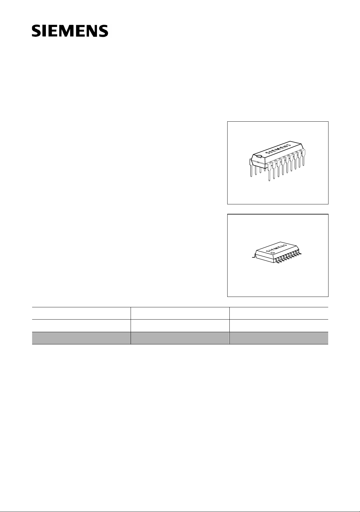
P-DIP-18-3
P-DSO-20-6
Type Ordering Code Package
TLE 4205 Q67000-A9025 P-DIP-18-3
TLE 4205 G Q67006-A9114 P-DSO-20-6
Description
TLE 4205 is an integrated power full-bridge DC-motor driver for a wide temperature
range, as required in automotive applications for example. The circuit contains two
power comparators that can be combined to a full-bridge circuit. For inductive loads
V
there are integrated free -wheeling diodes to +
and ground. The outputs are short-
S
circuit proof up to 18 V supply voltage to ground and turn off when overtemperature
occurs. This IC is especially suitable for headlight-beam adjustment in automobiles.
Semiconductor Group 1 1998-02-01
Page 2
TLE 4205
Q1
V
Q2
GND
ΙΙ-+
+Ι1
Ι1-
TLE 4205
1
2
S
3
4
5
2
6
2
7
8
9
18
17
16
15
14
13
12
11
10INH
AEP00636
GND
must be connected
to Pin 4
Q2
N.C.
N.C.
GND
GND
GND
GND
2
-
Ι
2+
Ι
Ι
+
1
TLE 4205 G
12
11
V
S
Q1
N.C.
GND
GND
GND
GND
N.C.
NH
Ι
Ι
-1
120
219
318
417
516
615
714
813
9
10
AEP01318
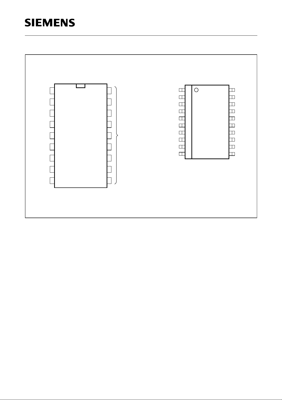
Figure 1 Pin Configuration (top view)
Semiconductor Group 2 1998-02-01
Page 3
Pin Definitions and Functions
Pin No. Symbol Function
1Q1Output Q1 of channel 1; push-pull B output with DC
short-circuit protection to ground. Integrated free-wheeling
diodes to ground and the supply voltage.
TLE 4205
2
V
S
Supply voltage VS; must be blocked to ground with a ceramic
capacitor of at least 100 nF directly on the pins of the IC.
3Q2Output Q2 of channel 2; see pin 1.
4 GND Ground
5 – I2 Inverting input channel 2; to be wired according to general
rules.
6 + I2 Non-inverting input channel 2; to be wired according to
general rules.
7 + I1 Non-inverting input channel 1; see pin 6.
8 – I1 Inverting input channel 1; see pin 5.
9INHInhibit; the IC is passive when this pin is open or connected to
ground.
10-18 GND Ground; must be connected to pin 4.
Semiconductor Group 3 1998-02-01
Page 4
TLE 4205
Pin Definitions and Functions (TLE 4205 G)
Pin No. Symbol Function
1Q2Output 2 of channel 2; push-pull B out put with DC shor t-circui t
protection to ground. Integrated free-wheeling diodes to ground
and the supply voltage.
2 N.C. Not connected
3 N.C. Not connected
4-7 GND Ground
8 – I2 Inverting input channel 2; to be wired according to general
rules.
9 + I2 Non-inverting input channel 2; to be wired according to
general rules.
10 + I1 Non-inverting input channel 1; see pin 9.
11 – I1 Inverting input channel 1; see pin 8.
12 INH Inhibit; the IC is passive when this pin is open or connected to
ground.
13 N.C. Not connected
14-17 GND Ground
18 N.C. Not connected
19 Q1 Output Q1 of channel 1, see pin 1.
20
V
S
Supply voltage VS; must be blocked with a ceramic capacitor
of at least 100 nF directly on the pins of the IC.
Semiconductor Group 4 1998-02-01
Page 5

TLE 4205
V
S
2 (20)
T1
7
1
+
1
ΙΙ-
(10)
8
(11)
+
-
1
(19)
Q1
T2
INH
+Ι
-Ι
2
2
9
(12)
6
(9)
5
(8)
Power Limiting
for T1, T3
Temperature
Protection
T3
+
-
(1)
3
Q2
T4
(4-7)
4, 10-18
(14-17)
GND
AEB00637
Figure 2 Block Diagram
Semiconductor Group 5 1998-02-01
Page 6

TLE 4205
Circuit Description
The IC contains two amplifiers with typical open-loop gain of 80 dB at 500 Hz.
The input stages consist of PNP-differenti al amplifi ers. This produ ces a common-m ode
V
input range of 0 V to nearly
guarded against ground sho rts by an SOA-prot ective circu it. The output t ransistors are
turned off if the chip temperature exc eeds approx. 160 °C. The IC can be turned off by
an inhibit input, which very much reduces current consumption.
and a maximum differential input voltage of VS. The IC is
S
V
S
(2)
+Ι
+
TLE 4205
Ωk10
(6)
2
(5)
2
-Ι
(8)
11ΙΙ-
10 kΩ
(7)
10 kΩ
Ωk10
Ωk10
(9)
INH
Ωk30
200
kΩ
(4)
GND
(10-18)
GND
(1)
(3)
AES00665
Q
Q
1
2
Figure 3 Circuit Diagram
Semiconductor Group 6 1998-02-01
Page 7

TLE 4205
Absolute Maximum Ratings
T
= − 40 to 150 °C
j
Parameter Symbol Limit Values Unit Remarks
min. max.
Supply voltage
Differential input voltage
Output current
Supply current
Ground current
Input voltage
Inhibit input
Junction temperature
Storage temperature
V
V
I
Q
I
S
I
GND
V
V
T
T
S
ID
I
Inh
j
stg
–0.3 45 V –
– ± V
S
V ∆V
6-5
TLE 4205
V
∆
8-9
TLE 4205 G
– 1 1 A –
2.5 3 A –
–3 2.5 A I2
–15 V
S
V V5; V6; V7; V
TLE 4205
V
; V9; V10; V
8
TLE 4205 G
–15 V
S
V V9 TLE 4205
V
TLE 4205G
12
– 150 °C–
– 50 150 °C–
or ∆V
or ∆V
7-8
10-11
8
11
Operating Range
Supply voltage
Case temperature
Case temperature
V
T
T
S
C
C
632V–
– 40 105 °C P
– 40 95 °C P
Thermal resistance
junction - ambient
junction - case
R
R
th JA
th JC
–
–
60
15
Thermal resistance
junction - ambient
junction - case
R
R
th JA
th JC
–
–
65
20
Outputs pin 1 (19) and pin 3 (1) short-circuit proof to GND at
(TLE 4205G)
= 3 W; DIP
Dmax
= 3 W; SO
Dmax
K/W
K/W
K/W
K/W
V
S
TLE 4205
TLE 4205
TLE 4205 G
TLE 4205 G
≤ 18 V for TLE 4205
Semiconductor Group 7 1998-02-01
Page 8

TLE 4205
Characteristics
V
6V <
Parameter Symbol Limit Values Unit Test Condition
General
< 18 V; – 40 °C < Tj < 150 °C
S
min. typ. max.
Open-circuit
current consumption
Open-circuit
current consumption
Turn-ON dead time
ref. to
V
9 OFF/ON
Turn-OFF dead time
ref. to
V
9 OFF/ON
Open-loop gain
Inputs
Input zero voltage
Input-voltage drift ∆
I
S
I
S
t
d ON
t
d OFF
G
VO
V
IO
V
/∆T –2030µV/K –
IO
– 10 30 mA active, both outputs
–10100µA inhibit
–1020µs|I
–1020µs|I
50 80 – dB f = 500 Hz
– 7.5 – 7.5 mV RS = 10 kΩ;
high
| < 1 A
1,3
TLE 4205
I
| < 1 A
|
1,19
TLE 4205 G
| < 1 A
1,3
TLE 4205
I
| < 1 A
|
1,19
TLE 4205 G
Input zero current
Input current
Input-current drift ∆
Input common-mode
I
IO
I
I
I
/∆T ––5nA/K–
I
V
IC
–75 – 75 mA –
– 300 – 300 nA –
––VS – 2 V –
range, positive
Input common-mode
V
IC
––– 0.5V–
range, negative
Power-supply
PSSR ––200µV/V R
= 10 kΩ;
S
rejection ratio
Common-mode
CMRR 70 80 – dB –
rejection ratio
Semiconductor Group 8 1998-02-01
Page 9

TLE 4205
Characteristics (cont’d)
6V <
Parameter Symbol Limit Values Unit Test Condition
Outputs
V
< 18 V; – 40 °C < Tj < 150 °C
S
min. typ. max.
Saturation voltage
Saturation voltage
Forward voltage of
free-wheeling diode
Forward voltage of
free-wheeling diode
Slew rate of
V
Q
Inhibit Input
Switching threshold
high
Switching threshold
low
H-input current
L-input current
Note: V
V
Sat U
Sat L
= upper
= lower
V
Sat U
V
Sat L
V
FU
V
FL
dVqdt
V
IH
V
IL
I
IH
I
IH
– 1.35 1.5 V IQ = – 0.6 A
–0.81.2VIQ = 0.6 A
–11.5VIF = 0.6 A
–11.5VIF = 0.6 A;
–0.5–V/µs–
r
2––V–
––0.8V–
–100–µA V9 = 5 V
–0–µA V9 = 0 V
Semiconductor Group 9 1998-02-01
Page 10

TLE 4205
V
S
V
9
V
5
V
6
Figure 4 Test Circuit
Ι
Q2
V
Q2
1000 µF
63 V
Ι
Q1
V
Q1
R
AES00638
470 nF
L
Ι
S
2
Ι
Ι
NH
9
Ι
-
Ι2
5
Ι
+ Ι2
6
Ι
- Ι1
8
Ι
+ Ι1
7
V
8
V
7
TLE 4205
4, 10-18
Ι
GND
1
3
2
100 µF 100 nF
V
Ι
NH
V
Ι1
+
V
- Ι1
V
- Ι2
V
+ Ι2
9
7
8
+
Amp 1
-
1
TLE 4205
5
6
-
Amp 2
+
3
220 nF
V
Q1
M
220 nF
V
Q2
4, 10-18
*) Value depends on load current and wiring inductivity
13.5 V
*)
Ω1
1Ω
AES00639
Figure 5 Application Circuit
Semiconductor Group 10 1998-02-01
Page 11

TLE 4205
Forward Voltage of the
Free-Wheeling Diodes versus
Junction Temperature
1.6
V
1.4
V
F
1.2
1.0
0.8
0.6
0.4
0.2
0
V
FU
V
FL
T
J
IED00955
Ι
= 0.6 A
F
˚C
Start Point of the SOAProtection Circuit versus
Junction Temperature
= 13.5 V
S
IED00956
˚C
12080400-40
2.4
A
2.0
I
1.6
V
1.2
0.8
0.4
12080400-40
0
T
J
Saturation Voltage versus
Junction Temperature
1.6
V
1.4
V
Sat
1.2
1.0
0.8
0.6
0.4
0.2
0
-40 0 40 80 120
V
V
Sat U
Sat L
I
= 600 mA
Q
V
= 13.5 V
S
T
J
IED00957
˚C
Current Consumption versus
Junction Temperature
18
mA
16
I
S
14
V
= 13.5 V
S
12
10
8
6
4
2
0
T
J
IED00958
12080400-40
˚C
Semiconductor Group 11 1998-02-01
Page 12

Package Outlines
P-DIP-18-3
(Plastic Dual In-line Package)
0.5 min
4.2 max
7.6
TLE 4205
±0.2
0.25
+0.1
6.4
7.6
-0.2
+1.2
2.54
1.5 max
0.45
+0.1
~
~
1.2
±0.3
3.5
18x0.25
1018
19
Index Marking
22.7
-0.2
0.4 max
GPD05035
Sorts of Packing
Package outlines for tubes, trays etc. are contained in our
Data Book “Package Information”.
Dimensions in mm
Semiconductor Group 12 1998-02-01
Page 13

P-DSO-20-6
(Plastic Dual Small Outline Package)
1.27
+0.15
0.35
2)
0.2 24x
TLE 4205
0.35 x 45˚
-0.2
-0.1
0.2
2.45
2.65 max
0.1
1120
7.6
10.3
-0.2
+0.8
0.4
±0.3
GPS05094
1)
+0.09
8˚ max
0.23
110
12.8
-0.2
1)
Index Marking
1) Does not include plastic or metal protrusions of 0.15 max per side
2) Does not include dambar protrusion of 0.05 max per side
Sorts of Packing
Package outlines for tubes, trays etc. are contained in our
Data Book “Package Information”.
SMD = Surface Mounted Device
Dimensions in mm
Semiconductor Group 13 1998-02-01
 Loading...