

Page 1
4-A DC Motor Driver
TLE 4203
Overview Bipolar IC
Features
• Integrated free-wheeling diodes
V
• Outputs short-circuit proof to
and ground
S
• Thermal overload protection
• Blocking of the output stages upon undervoltage
• Final push-pull stage free of cross-over
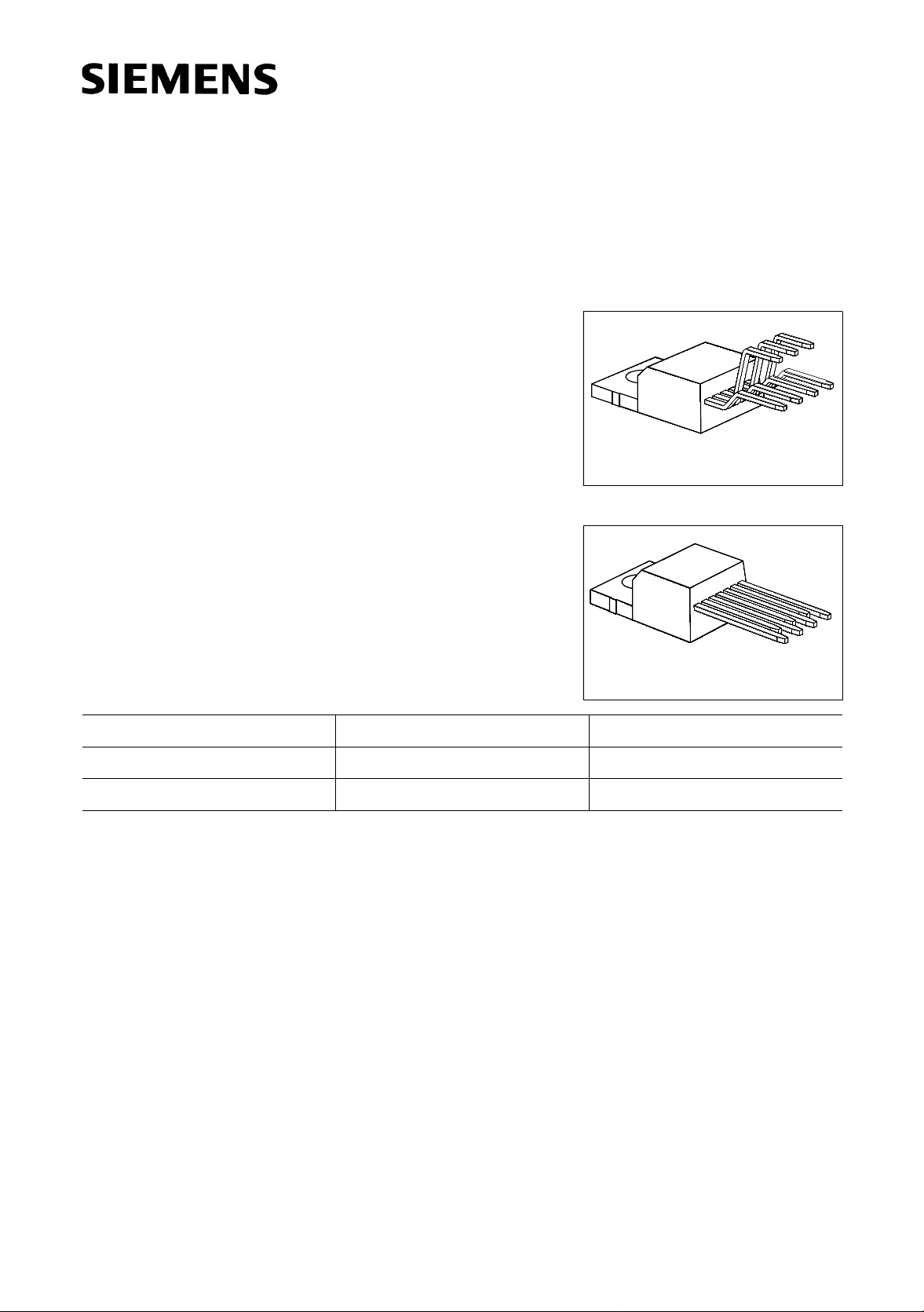
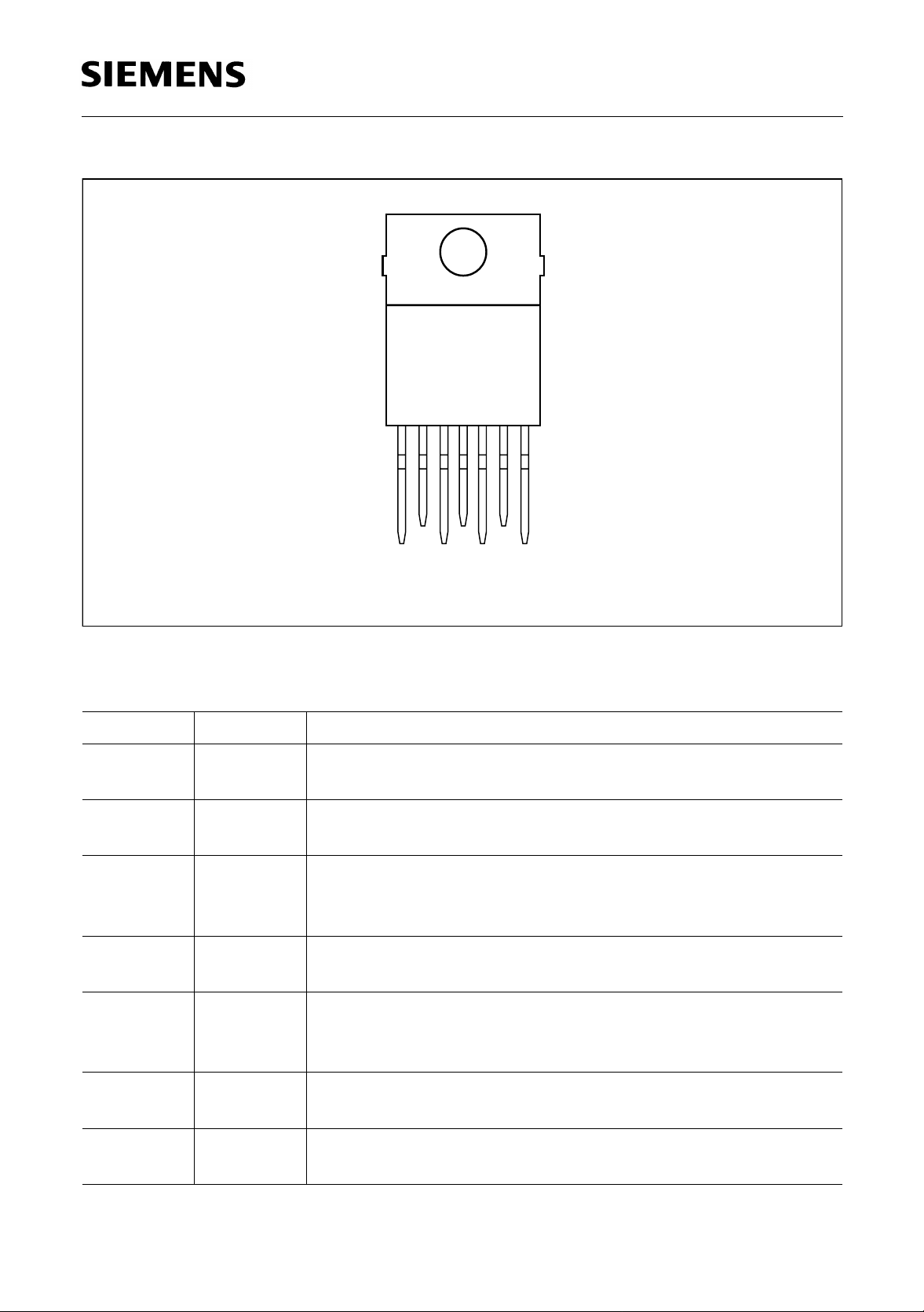
P-TO220-7-1
P-TO220-7-2
Type Ordering Code Package
TLE 4203 Q67000-A8121 P-TO220-7-1
TLE 4203 S Q67000-A9101 P-TO220-7-2
Description
The integrated circuit TLE 4203 is a versatile double power driver of up to 4 A output
current which is particularly suitable as a driver for DC motors in reversible operation.
The push-pull power output stages operate in the switching mode and can be combined
to a full-bridge configuration.
The drive of the input stage is implemented using digital logic.
The device contains a temperature protection logic, output stages protected against
short-circuit and integrated free-wheel ing dio des .
Typical applications are for follow-up control, servo drives, servo motors, drive
mechanisms, etc.
Semiconductor Group 1 1998-02-01
Page 2
TLE 4203
.
4321567
GND
V
S1 S2
IST1 Q1
V
Q2 IST2
AEP00618
Figure 1 Pin Configuration (top view)
Pin Definition and Functions
Pin No. Symbol Function
1IST1Control input for channel 1 (TTL/CMOS-compatible), of
non-inverting effect on the channel output.
2
V
S1
Channel 1 supply voltage; externally connected with the
supply voltage pin for channel 2 (pin 6).
3Q1Short-circuit protected push-pull C output channel 1 for
currents up to 6 A. Free-wheeling diodes are integrated on
chip for inductive loads.
4GND 1, 2Ground; track should be designed for the max. short-circuit
current (2 x 6 A).
5Q2Short-circuit protected push-pull C output channel 2 for
currents up to 6 A. Free-wheeling diodes are integrated on
chip for inductive loads.
6
V
S2
Channel 2 supply voltage; externally connected with the
supply voltage pin for channel 1 (pin 2).
7IST2Control input for channel 2 (TTL/CMOS-comp ati ble), of
non-inverting effect on the channel output.
Semiconductor Group 2 1998-02-01
Page 3
TLE 4203
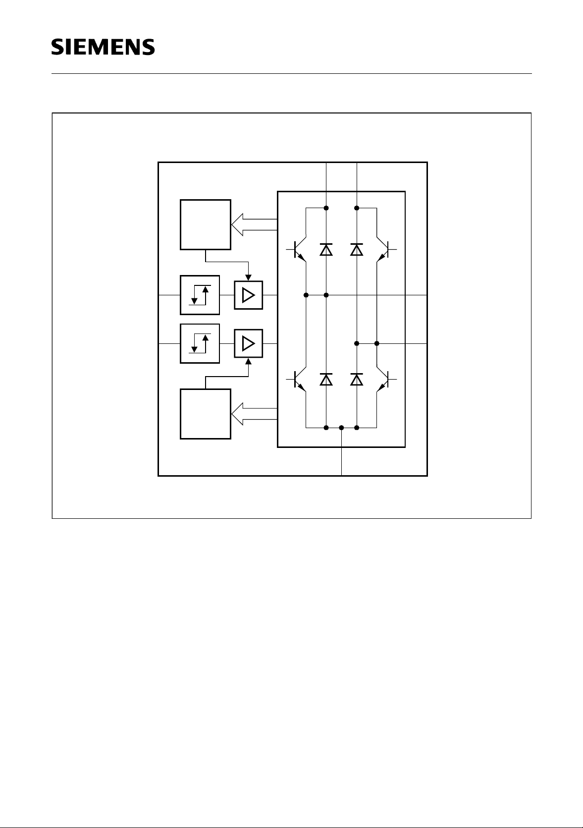
Control
Input 1
Control
Input 2
1
7
Protection
Circuit 1
Protection
Circuit 2
Supply Voltage
2
V
6
S
3
Output 1
5
Output 2
Figure 2 Block Diagram
4
GND
AEB00628
Semiconductor Group 3 1998-02-01
Page 4
TLE 4203
Application
In industrial and automotive electronics, power ful l-bridge DC motor dri vers are mostly
used for bidirectional motor drives. The two TTL and CMOS-compatible control inp uts
act on the output as follows:
Status Input 1 Input 2 Output 1 Output 2
1LL
2LHV
3HLV
4HHV
V
means: Lower power unit conducting; upper power unit blocked.
QL
V
means: Upper power unit conducting; lower power unit blocked.
QH
V
QL
QL
QH
QH
The following examples illustrate the operation:
Status 1: Motor is slowed down
Status 2: Motor turns right
Status 3: Motor turns left
Status 4: Motor is slowed down
V
V
V
V
QL
QH
QL
QH
Semiconductor Group 4 1998-02-01
Page 5

TLE 4203
Circuit Description
Input Circuit
The control inputs consist of TTL and CMOS-compatible Schmitt triggers with hysteresis.
Buffer amplifiers, controlled from thes e stages, convert the logic signal into the form
required for driving the power output stages.
Output Stages
The output stages consist of two push-pull C stages. Using protective circuits for limiting
the power dissipation makes the outputs short-circuit proof to ground and to supply
voltage throughout the entire operating range. Positive and negative voltage peaks,
which occur when switching inductive loads, are limited by integrated power diodes.
Monitoring and Protecting Functions
The IC is protected against thermal overloads by a temperature protecting circuit.
In addition an internal circuit en sures that all output transistors are bl ocked for supply
voltages below operating range.
A monitoring stage logic f or each output stage transistor dete cts whether the relevant
transistor is active and i n this case for sink operation (source operation) prevents the
corresponding source transistor (sink transistor) from being turned on. Direct cross-over
currents are effectively prevented with this method.
Semiconductor Group 5 1998-02-01
Page 6

TLE 4203
Absolute Maximum Ratings
T
= – 40 to 125 °C
C
Parameter Symbol Limit Values Unit
min. max.
Voltages
Supply voltage
Logic input voltages
Currents
Supply current
T
≤ 85 °C
C
Output current
T
≤ 85 °C
C
Ground current
T
≤ 85 °C
C
Temperatures
Junction temperature
Storage temperature range
Thermal resistances
system - case
system - ambient
V
S
V
I 1, 2
I
S
I
Q 1, 2
I
GND
T
j
T
stg
R
th SC
R
th SA
–0.3
–45
–12
–6
–12
–
–50
–
–
45
45
12
6
12
150
150
3
65
V
V
A
A
A
°C
°C
K/W
K/W
Operating Range
Supply voltage
Logic input voltage
Case temperature
T
≤ 150 °C
j
V
V
T
S
I 1, 2
C
5
–10
20
40
V
V
–40 125 °C
Semiconductor Group 6 1998-02-01
Page 7

Characteristics
V
= 8 to 18 V, Tj = – 25 to 125 °C (typ. VS = 12 V; Tj = 25 °C)
S
Parameter Symbol Limit Values Unit Test Condition
min. typ. max.
General Characteristics
TLE 4203
Quiescent current
Quiescent current
I
q
I
q
Logic
Control inputs
H-input voltage
L-input voltage
Hysteresis of
V
V
∆V
IH
IL
I
input voltage
H-input current
L-input current
V
= 8 to 18 V, TC = – 25 to 125 °C
S
I
IH
– I
IL
Switching Stages
Saturation voltages
V
to +
to + V
to + V
S
S
S
to ground
to ground
to ground
V
V
V
V
V
V
QSato
QSato
QSato
QSatu
QSatu
QSatu
–
–
2.8
–
–
–
–
–
–
–
–
–
–
70
180
–
–
0.7
–
–
1.1
1.5
2.5
0.3
0.6
1.6
100
230mAmA
–
1.2
–
10
10
1.3
1.8
3.5
0.6
1
3.2
V
V
V
µA
µA
V
V
V
V
V
V
V
V
= V
I1
= V
I1
I2
I2
> V
< V
–
–
–
V
= 5 V
I
V
= 0.5 V
I
V
> VIH; IQ = – 1 A
I 1, 2
V
> VIH; IQ = – 2 A
I 1, 2
V
> VIH; IQ = – 4 A
I 1, 2
V
< VIL; IQ = 1 A
I 1, 2
V
< VIL; IQ = 2 A
I 1, 2
V
< VIL; IQ = 4 A
I 1, 2
IH
IL
1)
1)
1)
Forward Voltages
Diode to +
Diode to + V
Diode of + V
V
S
S
S
Diode to ground
Diode to ground
Diode to ground
1)
measured to + V
Semiconductor Group 7 1998-02-01
S
–
V
– V
– V
– V
– V
– V
QFo
QFo
QFo
QFu
QFu
QFu
–
–
–
–
–
–
0.95
1.05
1.30
0.95
1
1.20
1.3
1.5
1.8
1.3
1.5
1.8
V
V
V
V
V
V
V
> VIH; IQ = 1 A
I 1/ 2
V
> VIH; IQ = 2 A
I 1/ 2
V
> VIH; IQ = 4 A
I 1/ 2
V
< VIL; IQ = – 1 A
I 1/ 2
V
< VIL; IQ = – 2 A
I 1/ 2
V
< VIL; IQ = – 4 A
I 1/ 2
1)
1)
1)
Page 8

TLE 4203
Ι
,
Ι
q
S
4700 µF
63 V
470 nF
V
S
V
Ι1
Figure 3 Test Circuit
V
=
V
Ι1
Ι2
4203
4
Ι
M
6
Ι
3
5
Q1
Ι
Q2
VV
Q2
Q1
AES00620
R
L
2
Ι
1
Ι
1
TLE
Ι
Ι
2
7
V
Ι2
_
<
t
=
t
100 ns
r
V
ΙH
V
ΙL
f
t
t
d
t
Ι
Q2
t
t
d
0
t
4 A
-4 A
t
AET00621
Figure 4 Timing Diagram
Semiconductor Group 8 1998-02-01
Page 9

TLE 4203
+
V
= 12 V
S
220 nF
Control
Inputs
Figure 5 Application Circuit
1000 µF
1
7
2
TLE
4203
4
Ω
1
6
220 nF
3
M
5
220 nF
1
Ω
AES00622
Semiconductor Group 9 1998-02-01
Page 10

TLE 4203
Saturation Voltage versus
Output Current
250
Ι
Q
mA
200
V
V
1/2<Ι
150
V
V
Ι=1
100
V
V
50
Ι>1/2
V
R
Ι L
2Ι
HΙ
=12 V
S
=2.4 Ω
L
AED00623
Short-Circuit Current versus
Output Voltage
V
= VQ for sink operation
A
V
= VS – VQ for source operation
A
6
Ι
Q
A
5
= 25 ˚C
T
C
4
3
2
1
AED00625
0
-50 0 50 100
Saturation Voltage versus
Output Current
3.0
V
Q
V
2.0
1.5
1.0
0.5
T
V
Q Sato
V
= 25 ˚C
C
SatuQ
150 ˚C 200
T
j
AED00624
0
0
10 20 30 40
Diode Forward Voltage versus
Output Current
1.4
V
Q
V
1.0
0.8
0.6
0.4
0.2
V
Q
V
T
Fo
FuQ
= 25 ˚C
C
V
V
Q
AED00626
0.0
0
1 2
3
4
5
A
Ι
Q
0.0
0
1 2
3
4
5
A
Ι
Q
Semiconductor Group 10 1998-02-01
Page 11

Package Outlines
P-TO220-7-1
(Plastic Transistor Single Outline)
TLE 4203
+0.4
10
10.2
-0.2
+0.1
3.75
2.8
17
1.27
1)
+0.1
0.6
1) 0.75
1) 0.75
at dam bar (max 1.8 from body)
-0.15
im Dichtstegbereich (max 1.8 vom Körper)
-0.15
0.6
7x
4.6
-0.2
1 x 45˚
+0.1
1.27
±0.3
-0.2
±0.4
19.5 max
16
2.6
+0.1
0.4
±0.4
M
4.5
8.4
±0.4
8.8
15.4
±0.3
±0.3
8.6
10.2
GPT05108
Sorts of Packing
Package outlines for tubes, trays etc. are contained in our
Data Book “Package Information”.
Dimensions in mm
Semiconductor Group 11 1998-02-01
Page 12

P-TO220-7-2
(Plastic Transistor Single Outline)
+0.4
10
10.2
-0.2
+0.1
3.75
17
2.8
11
13
1.27
+0.1
4.6
-0.2
1 x 45˚
-0.2
8.8
TLE 4203
15.4
1.27
1) 0.75
1) 0.75
+0.1
1)
0.6
0.6
M
7x
at dam bar (max 1.8 from body)
-0.15
im Dichtstegbereich (max 1.8 vom Körper)
-0.15
0.4
2.6
+0.1
GPT05257
Sorts of Packing
Package outlines for tubes, trays etc. are contained in our
Data Book “Package Information”.
Dimensions in mm
Semiconductor Group 12 1998-02-01
 Loading...