

Page 1

February 1999 TOKO, Inc. Page 1
ADVANCED INFORMATION
FEATURES
■ Low Dropout Voltage
■ Very Low Quiescent Current (50 µA maximum)
■ Internal Bandgap Reference
■ Regulates down to 1.8 V
■ Short Circuit Protection
■ Very Low Standby Current (1 µA maximum)
■ Miniature Package (SOT-23-5)
BLOCK DIAGRAM
TKxxxxx
GND
V
IN
NC
V
OUT
CONTROL
TK6xxxx S
ORDERING INFORMATION
TAPE/REEL CODE
TL: Tape Left
PACKAGE CODE
S: SOT-23-5
Tape/Reel Code
Package Code
VOLTAGE CODE
18 = 1.8 V 33 = 3.3 V 55 = 5.5 V
20 = 2.0 V 35 = 3.5 V 60 = 6.0 V
25 = 2.5 V 40 = 4.0 V
28 = 2.8 V 45 = 4.5 V
30 = 3.0 V 50 = 5.0 V
Voltage Code
DESCRIPTION
The device is a low dropout linear regulation housed in a
small SOT-23-5 package, rated at 500 mW.
An internal P Channel pass transistor is used in order to
achieve low dropout voltage. The device has extremely
low quiescent current (max 50 µA). The device offers high
precision output voltage of 2% at over temperature. The
low quiescent current and dropout voltage make this part
ideal for battery powered applications. In the standby
mode when the device is disabled, the linear regulator only
draws 1 µA (max).
APPLICATIONS
■ Battery Powered Systems
■ Cellular Telephones
■ Pagers
■ Toys
■ Radio Control Systems
■ Low Voltage Systems
■ Personal Communications Systems
■ Portable Instrumentation
■ Portable Consumer Equipment
CMOS LDO REGULATOR WITH HIGH ACTIVE CONTROL
ADVANCED
INFORMATION
CONTROL
GND
V
IN V
OUT
+
-
BANDGAP
REFERENCE
CONTROL
CIRCUIT
+
-
CURRENT
LIMIT
Page 2
Page 2 February 1999 TOKO, Inc.
ADVANCED INFORMATION
ABSOLUTE MAXIMUM RATINGS
All pins except GND ................................................... 9 V
Power Dissipation (Note 1) ................................ 500 mW
Storage Temperature Range ................... -55 to +150 °C
Operating Temp. Range..............................-30 to +80 °C
Junction Temperature ........................................... 150 °C
ELECTRICAL CHARACTERISTICS
Test conditions: VIN = V
OUT(TYP)
+ 1 V, TA = 25 °C, unless otherwise specified.
Note 1: Power dissapation is 500 mW when mounted as recommended (150 mW in Free Air). Derate at 1.8 mW/°C for operation above 25 °C.
Note 2: V
OUT
= 1.8 V to 6 V, 0.1 V step.
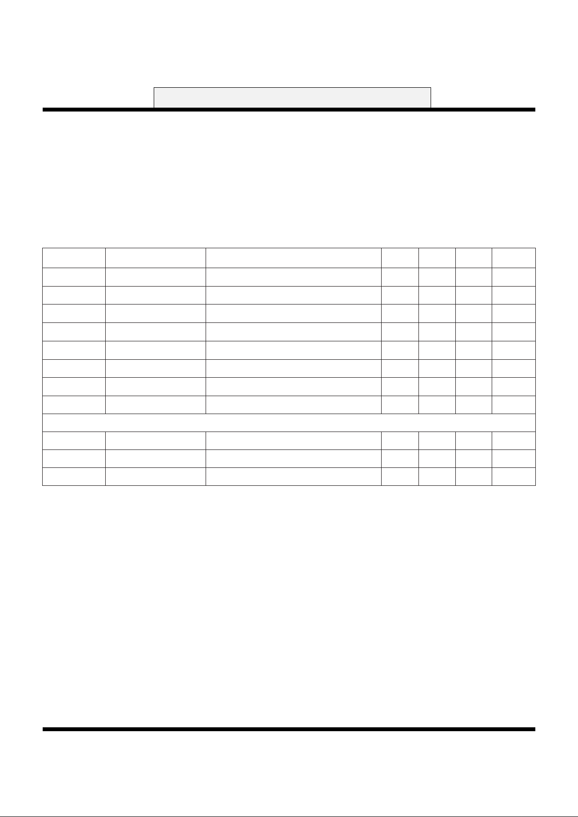
LOBMYSRETEMARAPSNOITIDNOCTSETNIMPYTXAMSTINU
V
NI
ylppuStupnI 8V
I
Q
tnerruCtnecseiuQdaoLoN0305Aµ
I
YBTS
tnerruCybdnatSVNIffOtuptuO,V8=1Aµ
I
TUO
tnerruCtuptuO05Am
V
TUO
egatloVtuptuOT,2etoN
A
I,C°08+ot03-=
TUO
Am1=%2-V
TUO
%2V
geRdaoLnoitalugeRdaoLI
TUO
Am1=Am05ot002Vm
geReniLnoitalugeReniLV
)PYT(TUO
V5.0+ ≤ VNI≤ I,V8
TUO
Am1=DBTVm
V
PORD
egatloVtuoporDI
TUO
Am05=55002Vm
SNOITACIFICEPSLANIMRETLORTNOC
I
TNOC
tnerruClortnoCV
TNOC
NOtuptuO,V5.1=DBTAµ
V
TNOC
)NO(NOegatloVlortnoCNOtuptuO5.1V
V
TNOC
)FFO(FFOegatloVlortnoCFFOtuptuO52.0V
Page 3

February 1999 TOKO, Inc. Page 3
ADVANCED INFORMATION
DEFINITION AND EXPLANATION OF TECHNICAL TERMS
OUTPUT VOLTAGE (V
OUT
)
The output voltage is specified with VIN = (V
OUT(TYP)
+ 1 V)
and I
OUT
= 1 mA.
DROPOUT VOLTAGE (V
DROP
)
The dropout voltage is the difference between the input
voltage and the output voltage at which point the regulator
starts to fall out of regulation. Below this value, the output
voltage will fall as the input voltage is reduced. It is
dependent upon the load current and the junction
temperature.
OUTPUT CURRENT (I
OUT
)
Normal operating output current. This is limited by package
power dissipation.
LINE REGULATION (Line Reg)
Line regulation is the ability of the regulator to maintain a
constant output voltage as the input voltage changes. The
line regulation is specified as the input voltage is changed
from VIN = V
OUT
+ 0.5 V to VIN = 8 V.
LOAD REGULATION (Load Reg)
Load regulation is the ability of the regulator to maintain a
constant output voltage as the load current changes. It is
a pulsed measurement to minimize temperature effects
with the input voltage set to VIN = V
OUT
+1 V. The load
regulation is specified under output current step conditions
of 1 mA to 50 mA.
QUIESCENT CURRENT (IQ)
The quiescent current is the current which flows through
the ground terminal under no load conditions (I
OUT
= 0 mA).
STANDBY CURRENT (I
STBY
)
Standby current is the current which flows into the regulator
when the output is turned off by the control function
(V
CONT
= 0 V). It is measured with VIN = 8 V.
SENSOR CIRCUITS
Overcurrent Sensor
The overcurrent sensor protects the device if the output is
shorted to ground.
PACKAGE POWER DISSIPATION (PD)
This is the power dissipation level at which the thermal
sensor is activated. The IC contains an internal thermal
sensor which monitors the junction temperature. When the
junction temperature exceeds the monitor threshold of
150 °C, the IC is shut down. The junction temperature
rises as the difference between the input power (VIN x IIN)
and the output power (V
OUT
x I
OUT
) increases. The rate of
temperature rise is greatly affected by the mounting pad
configuration on the PCB, the board material, and the
ambient temperature. When the IC mounting has good
thermal conductivity, the junction temperature will be low
even if the power dissipation is great. When mounted on
the recommended mounting pad, the power dissipation of
the SOT-23-5 is increased to 500 mW. For operation at
ambient temperatures over 25 °C, the power dissipation of
the SOT-23-5 device should be derated at 4.0 mW/ °C. To
determine the power dissipation for shutdown when
mounted, attach the device on the actual PCB and
deliberately increase the output current (or raise the input
voltage) until the thermal protection circuit is activated.
Calculate the power dissipation of the device by subtracting
the output power from the input power. These
measurements should allow for the ambient temperature
of the PCB. The value obtained from PD /(150 °C - TA) is the
derating factor. The PCB mounting pad should provide
maximum thermal conductivity in order to maintain low
device temperatures. As a general rule, the lower the
temperature, the better the reliability of the device. The
thermal resistance when mounted is expressed as follows:
Tj = 0jA x PD + T
A
For Toko ICs, the internal limit for junction temperature is
150 °C. If the ambient temperature (TA) is 25 °C, then:
150 °C = 0jA x PD + 25 °C
0jA = 125 °C / P
D
Page 4

Page 4 February 1999 TOKO, Inc.
ADVANCED INFORMATION
DEFINITION AND EXPLANATION OF TECHNICAL TERMS (CONT.)
PD is the value when the thermal protection circuit is
activated. A simple way to determine PD is to calculate V
IN
x IIN when the output side is shorted. Input current gradually
falls as temperature rises. You should use the value when
thermal equilibrium is reached.
The range of usable currents can also be found from the
graph below.
Procedure:
1) Find P
D
2) PD1 is taken to be PD x (~0.8 - 0.9)
3) Plot PD1 against 25 °C
4) Connect P
D1
to the point corresponding to the 150 °C
with a straight line.
5) In design, take a vertical line from the maximum
operating temperature (e.g., 75 °C) to the derating
curve.
6) Read off the value of PD against the point at which the
vertical line intersects the derating curve. This is taken
as the maximum power dissipation, DPD.
The maximum operating current is:
I
OUT
= (D
PD
/ (V
IN(MAX) - VOUT
)
SOT-23-5 POWER DISSIPATION CURVE
P
D
D
PD
25 50 75 150
(mW)
TA (°C)
3
6
5
4
0 50 100 150
TA (°C)
P
D
(
m
W)
0
100
500
MOUNTED AS
SHOWN
FREE AIR
200
300
400
Page 5

February 1999 TOKO, Inc. Page 5
ADVANCED INFORMATION
APPLICATION INFORMATION
+
CONTROL
V
IN
V
OUT
+
GND
BOARD LAYOUT
SOT-23-5 BOARD LAYOUTBAOR-5
Page 6

Page 6 February 1999 TOKO, Inc.
ADVANCED INFORMATION
0.95
0.95
0.950.95
e
M
0.1
2.9
1.6
1.1
0.15
0.4
2.8
1.90
2.4
e'
Recommended Mount Pad
1
23
45
1.0
0.7
(0.8)
0 - 0.1
(0.6)
(0.6)
1.4 max
e
e e
0.1
e1
0 - 15 max
Marking
± 0.3
+0.15
- 0.05
Dimensions are shown in millimeters
Tolerance: x.x = ± 0.2 mm (unless otherwise specified)
+0.15
-0.05
Marking Information
Part Number Marking
SOT-23-5
PACKAGE OUTLINE
Printed in the USA
© 1999 Toko, Inc.
All Rights Reserved
TOKO AMERICA REGIONAL OFFICES
Toko America, Inc. Headquarters
1250 Feehanville Drive, Mount Prospect, Illinois 60056
Tel: (847) 297-0070 Fax: (847) 699-7864
IC-216-TKxxxxx
0798O0.0K
Visit our Internet site at http://www.tokoam.com
The information furnished by TOKO, Inc. is believed to be accurate and reliable. However, TOKO reserves the right to make changes or improvements in the design, specification or manufacture of its
products without further notice. TOKO does not assume any liability arising from the application or use of any product or circuit described herein, nor for any infringements of patents or other rights of
third parties which may result from the use of its products. No license is granted by implication or otherwise under any patent or patent rights of TOKO, Inc.
Western Regional Office
Toko America, Inc.
2480 North First Street , Suite 260
San Jose, CA 95131
Tel: (408) 432-8281
Fax: (408) 943-9790
Midwest Regional Office
Toko America, Inc.
1250 Feehanville Drive
Mount Prospect, IL 60056
Tel: (847) 297-0070
Fax: (847) 699-7864
Eastern Regional Office
Toko America, Inc.
107 Mill Plain Road
Danbury, CT 06811
Tel: (203) 748-6871
Fax: (203) 797-1223
Semiconductor Technical Support
Toko Design Center
4755 Forge Road
Colorado Springs, CO 80907
Tel: (719) 528-2200
Fax: (719) 528-2375
 Loading...