

Page 1
1
3
6
4
2
V
O
V
IN
GND
GND
SHUT DOWN
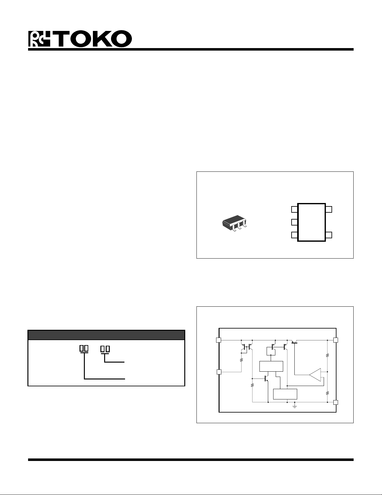
TK702xx
1.03 V REGULATOR WITH ON/OFF SWITCH
FEATURES
■ Low Input Voltage Operation (Single Battery Cell)
■ Internal PNP Transistor
■ Built-In Shutdown Control (Off Current, 8 µA Typ)
■ Low Dropout Voltage (30 mV Typ)
■ Very Small Surface Mount Package (SOT-25)
DESCRIPTION
The TK702xx is a very low dropout, low input voltage
operation regulator suitable for single battery cell applications. This regulator provides 1.03 V output with a dropout
voltage of only 30 mV. The active high control provides on/
off switching of the output. In the off mode, the standby
supply current is 8 µA, thus extending battery life.
The TK702xx is available in a very small plastic surface
mount package (SOT-25).
APPLICATIONS
■ Pagers
■ Personal Communication Equipment
■ Portable Consumer Equipment
■ Radio Control Systems
■ Single Battery Cell Systems
TK702xx
BLOCK DIAGRAM
ORDERING INFORMATION
V
6 4
IN
V
O
TK702 M
Tape/Reel Code
SHUT
1
Voltage Code
VOLTAGE CODE
03 = 1.03 V
January, 1996 TOKO, Inc. Page 1
TAPE/REEL CODE
BX : Bulk/Bag
TL : Tape Left
DOWN
1-16-96
SHUT DOWN
BANDGAP
REFERENCE
+
-
GND
2,3
TK70203 BD
Page 2
TK702xx
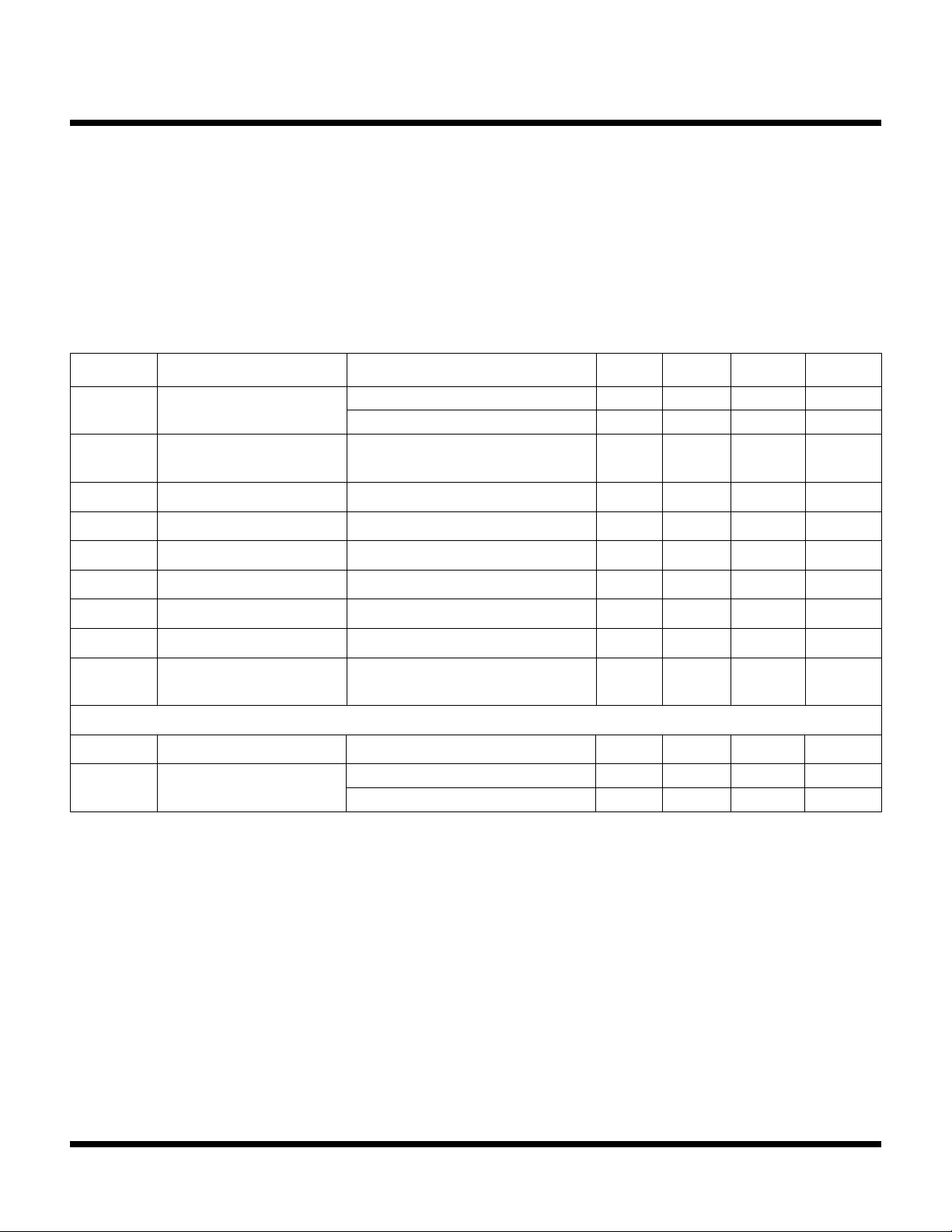
ABSOLUTE MAXIMUM RATINGS
Input Voltage..............................................................6 V
Power Dissipation ..............................................150 mW
Operating Voltage Range..............................0.9 to 5.0 V
Storage Temperature Range ...................-55 to +150 °C
Operating Temperature Range ..................-10 to +60 °C
Lead Soldering Temp. (10 sec.)......................... 240 °C
Junction Temperature .......................................... 150 °C
ELECTRICAL CHARACTERISTICS
Test Conditions: VCC = 1.4 V, T
SYMBOL PARAMETER TEST CONDITIONS MIN TYP MAX UNITS
I
IN
I
STBY
V
O
V
DROP
I
O
Supply Current
Standby Current V
Output Voltage IO = 2 mA 0.98 1.03 1.065 V
In/Out Voltage Drop IO = 2 mA 30 60 mV
Output Current Note 2 8 16 mA
Line Reg Line Regulation V
Load Reg Load Regulation I
RR Ripple Rejection 100 mVrms, f = 400 Hz, IO = 2 mA 36 dB
= 25 °C, unless otherwise specified.
A
IO = 0 mA 180 280 µA
V
= V
IN
= Off, 8 13 µA
OUT
- 50 mV, IO = 0 mA 400 800 µA
OUT
R = 820 kΩ, Note 1
= 1.4 → 1.7 V 10 30 mV
IN
= 0.1 → 5.0 mA, Note 3 5 20 mV
O
∆VO/∆TAOutput Voltage I
= 2 mA, TA = -10 to +50 °C 0.3 mV/°C
O
Temperature Dependency
Control Terminal Specification R = 820 kΩ (series connection)
I
CONT
V
CONT
Note 1: Standby current (including control current) is the input current with a 820kΩ connected in series with the control terminal.
Note 2: I
Note 3: Since the measurement (pulse measurement) is in a constant T
Control Current V
Control Voltage
(Load Current) is a output current value when VO drops down 0.2 V from VO at IO = 2 mA.
O
included.
= Off, V
OUT
V
= On, TA = -10 to +60 °CVCC - 0.2 V
OUT
V
= Off, TA = -10 to +60 °C0 V
OUT
= VCC - 1.4 V 2 µA
CONT
, the output change due to temperature change is not
J
CC
- 0.8 V
CC
V
Page 2 January, 1996 TOKO, Inc.
1-16-96
Page 3
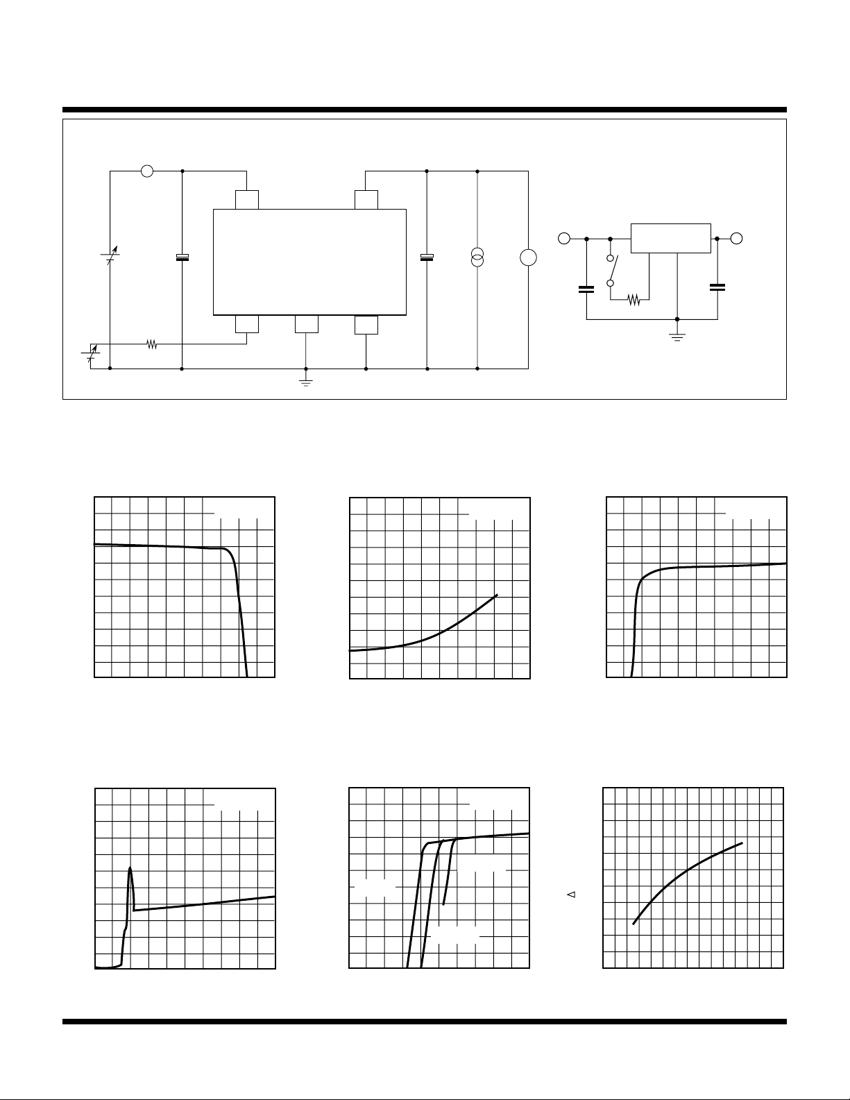
TK702xx
OUTPUT VOLTAGE vs.
V
(V)
O
V
I
0
F
OUT
IN
OUTPUT VOLTAGE vs.
V
(V)
INPUT CURRENT vs.
I
(mA)
OUTPUT VOLTAGE vs.
V
(V)
OUTPUT VOLTAGE DRIFT vs.
0
V
(mV)
INPUT CURRENT (NO LOAD) vs.
I
(µA)
TEST CIRCUIT
IN
A
1.05
O
1.0
V
IN
5 4
V
O
TK70203
820 kW
0.1
µF
+
SHUT
DOWN
1 2
GND
3
V
IN
SD
+
C
L
4.7
µF
V
I
O
V
C
.1 µF
Rc
= 3. 3 µ
L
TYPICAL PERFORMANCE CHARACTERISTICS
OUTPUT CURRENT
TA = 25 °C
OUTPUT CURRENT
1.0
TA = 25 °C
0.5
1.2
1.0
O
IN
SUPPLY VOLTAGE
TA = 25 °C
0.95
010
IO (mA)
INPUT VOLTAGE
500
IN
T
= 25 °C
A
20
1
0
01020
I
(mA)
O
2
SUPPLY VOLTAGE
1.05
TA = 25 °C
IO = 5.0 mA
O
1.0
IO = 0 mA
0.7
1.0
0.8 1.5 1.8
VIN (V)
+25
0
O
TEMPERATURE
IO = 2.5 mA
0
12 5
034
V
(V)
IN
4
January, 1996 TOKO, Inc. Page 3
0.95
0.9 1.0 1.3
0.8 1.1 1.2
VIN (V)
1-16-96
5
-30
-50 10
050
TEMPERATURE(°C)
3
6
Page 4
TK702xx
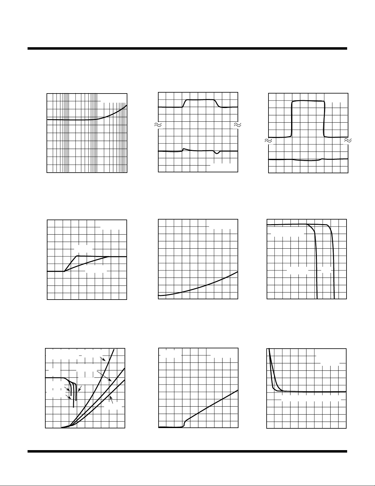
RIPPLE REJECTION
RIPPLE REJECTION (dB)
LINE TRANSIENT RESPONSE
1
LOAD TRANSIENT RESPONSE
1
SHORT CIRCUIT CURRENT
V
(V)
0
DROPOUT VOLTAGE vs.
V
(mV)
OUTPUT (ON/OFF)
V
NOISE SPECTRUM
NOISE (dB)
z
INPUT CURRENT vs.
I
(µA)
0
ON/OFF CONTROL TERMINAL
I
(µA)
.0
TYPICAL PERFORMANCE CHARACTERISTICS
0
-50
-100
SD
O
.1 1
TA = 25 °C
10
FREQUENCY (kHz)
CONTROL RESPONSE
TA = 25 °C
CL = 1 µF
CL = 3.3 µF
6.0
1.5
V
IN
I
O
TA = 25 °C
1.3
0
.05
V
100
O
1.01
TA = 25 °C
50 µ s/DIV
7
8
.05
V
O
1.01
50 µ s/DIV
9
OUTPUT CURRENT
200
TA = 25 °C
1.0
TA = 25 °C
0.8
0.6
O
100
DROP
0.4
VIN = 1.2 V
1.4 V
2.0
1.0
CONT
Page 4 January, 1996 TOKO, Inc.
(SERIES RESISTOR RC)
TA = 25 °C
V
OUT
RC = 500 k
RC = 820 k
0
0
V
10 µs/DIV
RC = 500 k
RC = 820 k
RC = 1 M
RC = 1 M
1.0 2
(V)
CONT
0.2
-50
0
0
10 2
IO (mA)
12
TA = 25 °C
0
10
12 5
034
I
(mA)
O
11
INPUT VOLTAGE
RC = 820 k
20
TA = 25 °C
IO = 3 mA
-100
10
N(OFF)
0
13
1.0 2.
VIN(V)
1-16-96
14
(SPECTRUM ANALYZER ONLY)
0
500 kHz 1 MH
FREQUENCY
15
Page 5
APPLICATION NOTES
D
G
V
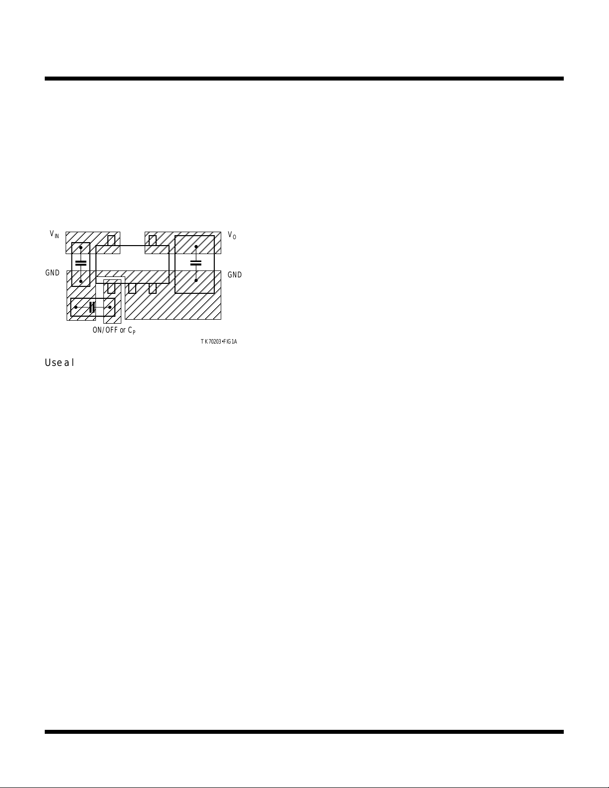
RECOMMENDED MOUNTING
Optimum performance can only be achieved when the IC
is mounted on a PC board according to the diagram below.
This is because of the extremely small package and limited
power dissipation. Shape the metal portion of the PCB as
shown in the following drawing.
TK702xx
V
GN
TK70203•FIG1A
O
ND
IN
ON/OFF o r C
P
Use a large bypass capacitor and connect it in a place near
GND of the IC. Pay attention to temperature characteristics
of the capacitor, especially the increase of ESR and decrease of capacitance in low temperatures. Oscillation,
reduction of ripple rejection and increased noise may occur
in some cases if the proper capacitor is not used. An output
capacitor more than 1.0 µF is required to maintain stability.
The standard test condition is 3.3 µF (TA = 25 °C).
DROPOUT VOLTAGE
Dropout voltage is the voltage difference between the input
voltage and the output voltage where the output voltage
decreases to 100 mV below the nominal output voltage as
the input voltage is decreased.
To measure dropout voltage, set the input voltage to the
nominal output voltage +1 V and measure the output
voltage. Reduce the input voltage to the point where the
output is 100 mV below the prevoiusly measured value.
The dropout voltage is the difference between the input and
ouput voltage at this point. This voltage depends on the
load current and ambient temperature.
January, 1996 TOKO, Inc. Page 5
1-16-96
Page 6
TK702xx
()
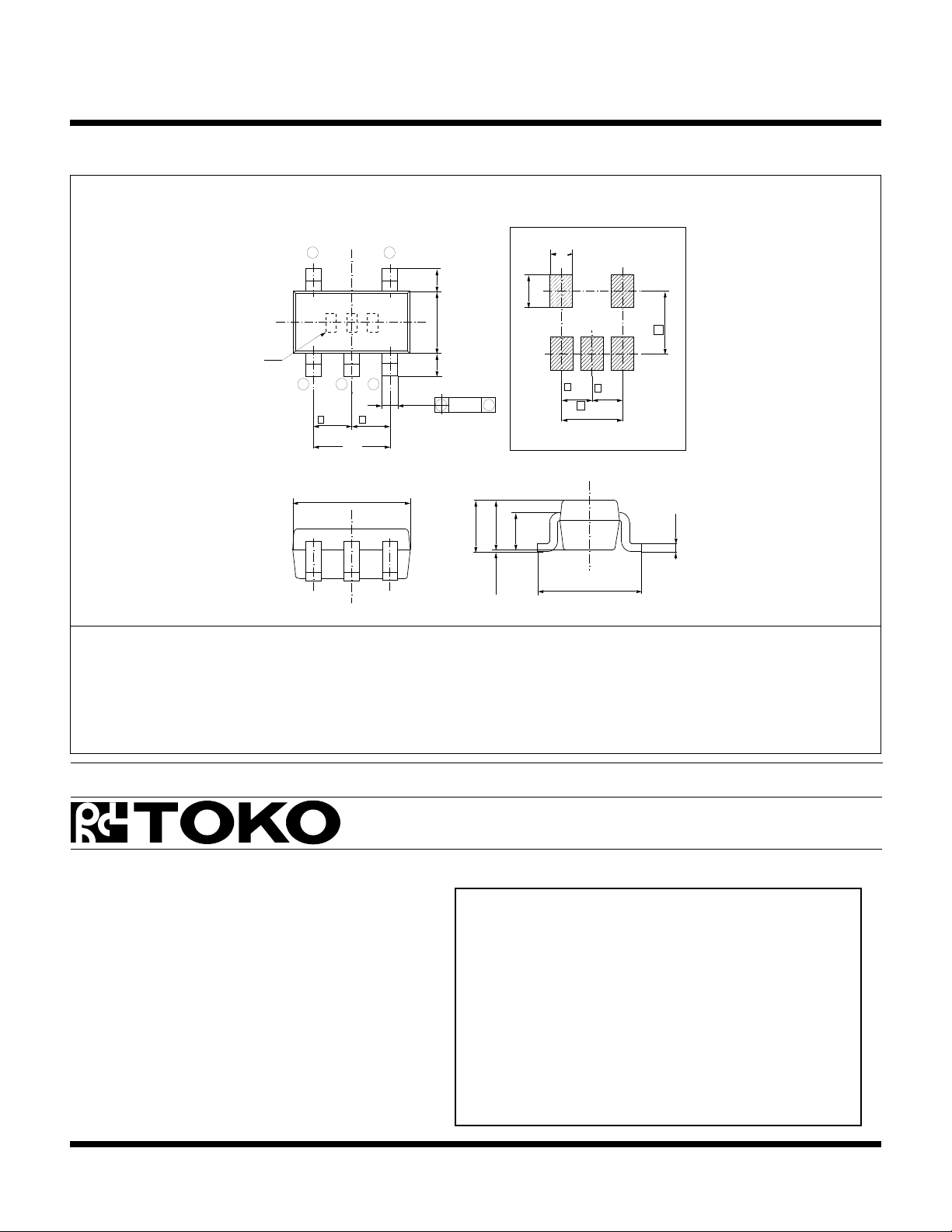
PACKAGE OUTLINE
SOT-25
Marking
Information
5 4
2 31
e
e
0.950.95
(1.9)
±
0.2
2.9
0.4
(0.6)(0.6)
-0.3
+0.2
1.6
±
0.1
0.1
1.3max
M
0.1
±
1.1
0 ~0.1
1.0
Recommended Mount Pad
0.8
Marking Information
TK70203 L03
0.7
e
0.95
2.6
1
e
e
0.95
e'
1.90
-0.05
+0.1
0.16
+0.2
-0.3
2.8
Unit:mm
The information furnished by TOKO, Inc. is believed to be accurate and reliable. However, TOKO reserves the right to make changes or improvements in the design, specification or manufacture of its products without
further notice. TOKO does not assume any liability arising from the application or use of any product or circuit described herein, nor for any infringements of patents or other rights of third parties which may result from the
use of its products. No license is granted by implication or otherwise under any patent or patent rights of TOKO, Inc.
YOUR LOCAL REPRESENTATIVE IS:
TOKO America, Inc.
1250 Feehanville Dr.
Mt. Prospect, IL 60056
Tel: 1(800) PIK-TOKO
Fax: 1(847) 699-1194
Page 6 January, 1996 TOKO, Inc.
© 1993 Toko America, Inc.
All Rights Reserved
Please order by literature number:
1-16-96
IC-136-TK70203
Printed in U.S.A.
 Loading...