

Page 1
TK70403
20P
1.03 V REGULATOR WITH ON/OFF SWITCH
FEATURES
■ Low Input Voltage Operation (Single Battery Cell)
■ Internal PNP Transistor
■ Internal Shutdown Control (Off Current, 0.1 µA max)
■ Low Dropout Voltage [30 mV (typ.) at 2 mA]
■ Miniature Package (SOT-26)
■ Very Low Noise
DESCRIPTION
TK70403 is a low dropout, linear regulator with a built-in
electronic switch. A pin for a bypass capacitor is provided,
which connects to the internal circuitry to lower the overall
output noise level.
An internal PNP pass-transistor is used in order to achieve
low dropout voltage (typically 30 mV at 2 mA load current).
This makes it possible to maintain a stable output voltage
as the battery voltage decreases, extending the useful
battery life.
APPLICATIONS
■ Pagers
■ Personal Communication Equipment
■ Portable Consumer Equipment
■ Radio Control Systems
■ Single Battery Cell Systems
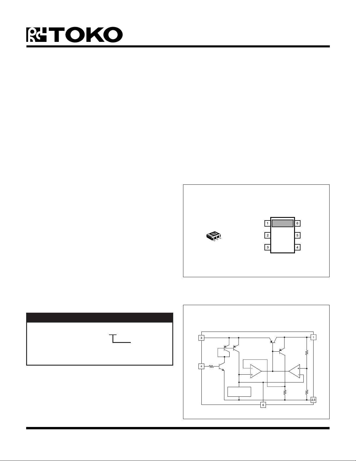
TK70403
V
OUT
GND
V
IN
NOISE
BYPASS
GND
CONTROL
The TK70403 is available in a miniature SOT-26 surface
mount package.
ORDERING INFORMATION
TK70403MTB
Tape/Reel Code
TAPE/REEL CODE
TB: Tape Left
V
CONTROL
BLOCK DIAGRAM
IN
BANDGAP
REFERENCE
NOISE
BYPASS
V
GND
OUT
January 1999 TOKO, Inc. Page 1
Page 2
TK70403
ABSOLUTE MAXIMUM RATINGS
Supply Voltage ........................................................... 6 V
Power Dissipation (Note 1) ................................ 350 mW
Junction Temperature ........................................... 150 °C
Storage Temperature Range ................... -55 to +150 °C
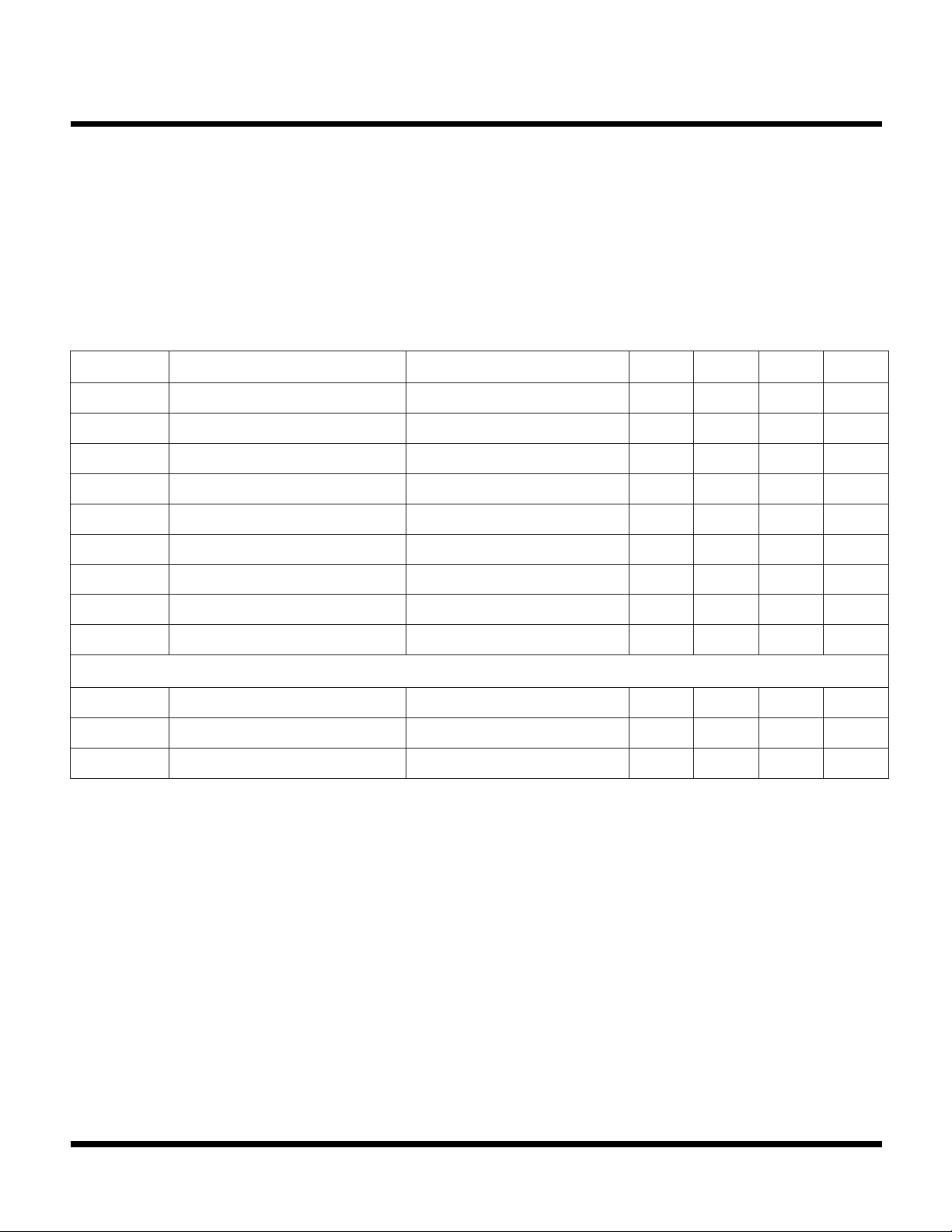
TK70403 ELECTRICAL CHARACTERISTICS
Test Conditions: VIN = 1.4 V, TA = 25 °C, R
LOBMYSRETEMARAPSNOITIDNOCTSETNIMPYTXAMSTINU
= 820 KΩ, unless otherwise specified.
CONT
Operating Temperature Range ...................-10 to +60 °C
Operating Voltage Range.............................. 0.9 to 5.0 V
Lead Soldering Temperature (10 s) ...................... 235 °C
I
YBTS
V
TUO
V
PORD
I
TUO
I
Q
geReniLnoitalugeReniLV
geRdaoLnoitalugeRdaoLI
/∆T
∆V
TUO
V
fer
I
TNOC
V
V
Note 1: Power dissipation is 350 mW when mounted as recommended. Derate at 2.8 mW/°C for operation above 25 °C.
Note 2: I
Gen Note: Ripple rejection and noise voltage are affected by the value and characteristics of the capacitor used. Example: Ripple rejection is 48
Gen Note: Parameters with min. or max. values are 100% tested at TA = 25 °C.
)NO(TNOC
)FFO(TNOC
when V
OUT
dB at CL = 1 µF, CN = 0.1 µF, I
drops 0.4 V from V
OUT
tnerruCybdnatSV
egatloVtuptuOI
egatloVtuoporDI
NI
TUO
TUO
Am2=89.030.1560.1V
Am2=60.0V
tnerruCtuptuO)2etoN(0105Am
tnerruCtnecseiuQI
tneiciffeoCerutarepmeTI
TUO
NI
TUO
TUO
Am2=52.0C°/Vm
egatloVecnerefeR4.0V
R:SNOITACIFICEPSLANIMRETLORTNOC
TNOC
tnerruClanimreTlortnoCV
K028= ΩΩΩΩΩ
TNOC
)NO(egatloVlortnoCNOtuptuO58.0V
)FFO(egatloVlortnoCFFOtuptuO03.0V
.
OUT(TYP)
= 2 mA, f = 400 Hz.
OUT
FFOtuptuO,V4.1=1.0Aµ
IgnidulcxE,Am0=
TNOC
051Aµ
V7.1ot34.1=02Vm
Am0.5ot1.0=02Vm
NOtuptuO,V0.1=0.1Aµ
Page 2 January 1999 TOKO, Inc.
Page 3
TK70403
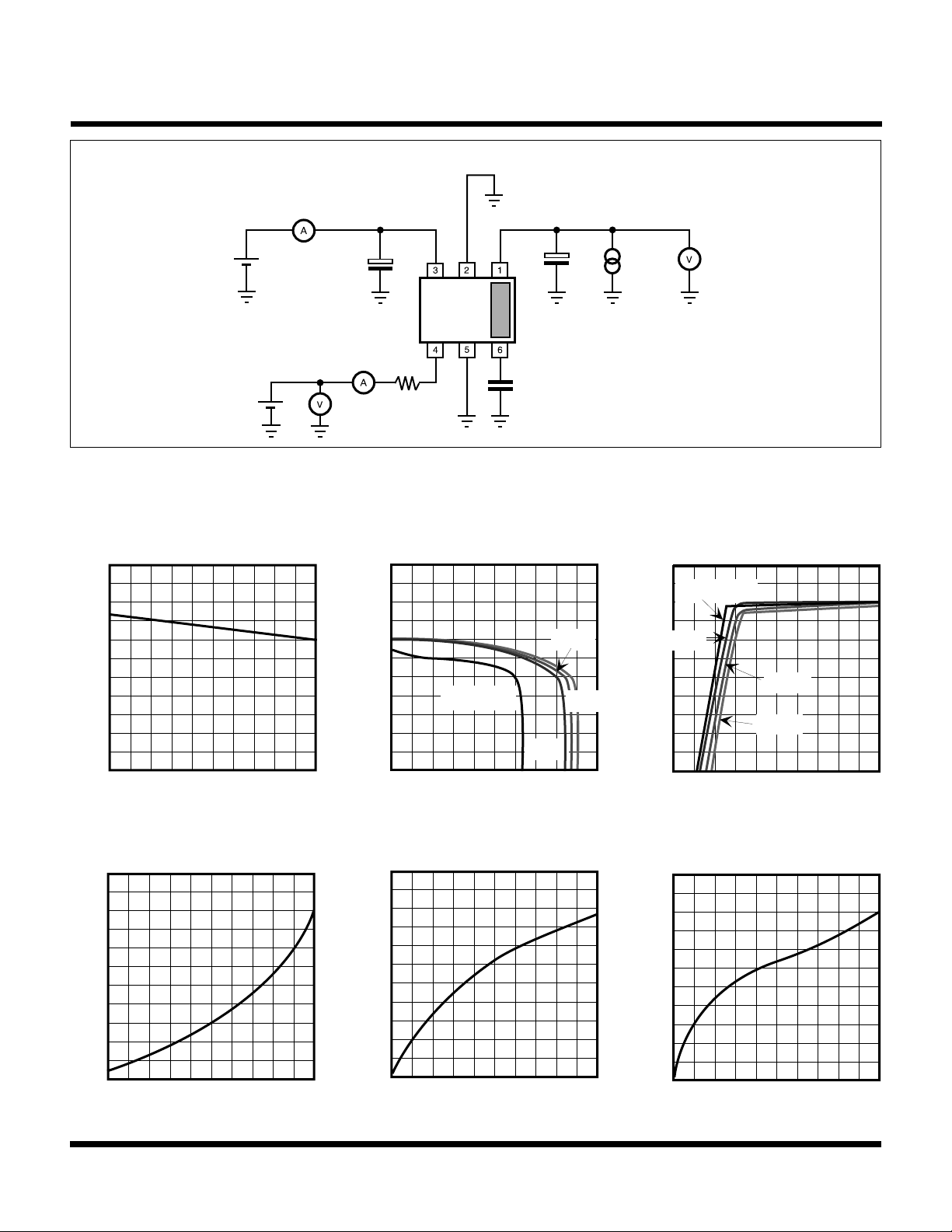
TEST CIRCUIT
I
IN
V
IN
GND
V
OUT
1 µF
V
IN
1 µF
I
OUT
V
OUT
V
CONT
TYPICAL PERFORMANCE CHARACTERISTICS
OUTPUT VOLTAGE VS.
OUTPUT CURRENT
1.05
1.04
(V)
1.03
OUT
V
1.02
1.01
0 5 10
I
(mA)
OUT
I
CONT
CONT
R
CONT
820 kΩ
GND
NOISE
BYPASS
C
N
0.1 µF
TA = 25 °C, unless otherwise specified.
OUTPUT VOLTAGE
OUTPUT CURRENT
1.5
1.2
(V)
0.9
OUT
V
0.6
VIN = 1.1 V
0.3
0
0 50 100
I
(mA)
OUT
VS.
1.4 V
1.6 V
1.2 V
OUTPUT VOLTAGE
INPUT VOLTAGE
1.08
I
= 0 mA
OUT
1.04
2.5 mA
(V)
1.00
OUT
V
0.96
0.92
5.0 mA
7.5 mA
0.8 1.0 1.2 1.4 1.6 1.8
VIN (V)
VS.
GROUND CURRENT VS.
OUTPUT CURRENT
2.5
2.0
1.5
(mA)
GND
I
1.0
0.5
0
0 10 20 30 40 50
I
(mA)
OUT
DROPOUT VOLTAGE
OUTPUT CURRENT
100
80
(mV)
60
DROP
40
V
20
0
0 2 4 6 8 10
I
(mA)
OUT
VS.
DROPOUT VOLTAGE VS.
OUTPUT CURRENT
200
(mV)
100
DROP
V
0
0 10 20 30 40 50
I
(mA)
OUT
January 1999 TOKO, Inc. Page 3
Page 4
TK70403
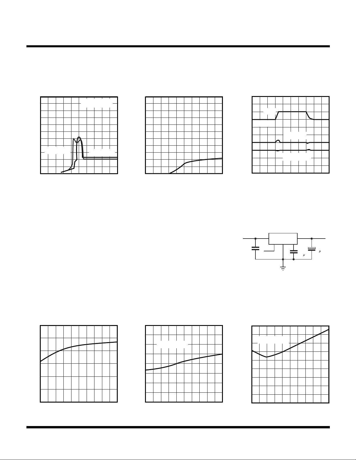
TYPICAL PERFORMANCE CHARACTERISTICS (CONT.)
TA = 25 °C, unless otherwise specified.
INPUT CURRENT
VS.
VOLTAGE (CONTROL ON)
500
I
OUT
400
300
(µA)
IN
I
200
TA = 60 °C
100
0
0 1 2
VIN (V)
INPUT
= 0 mA
TA = 25 °C
INPUT CURRENT
VOLTAGE (CONTROL OFF)
200
(pA)
100
IN
I
0
0 1 2
VIN (V)
VS.
INPUT
LINE VOLTAGE STEP RESPONSE
1.5 V
IN
V
1.4 V
CN = 0 µF
(10 mV/ DIV)
OUT
OUT
V
V
CN = 0.1 µF
TIME (50 µS/DIV)
V
IN
V
TK70403
CONT
V
OUT
C
C
0.1
L
1
N
F
F
RIPPLE REJECTION CIRUIT
OUTPUT CURRENT
TEMPERATURE
60
VS.
2.0
CONTROL CURRENT
TEMPERATURE
VS.
DROPOUT VOLTAGE
TEMPERATURE
VS.
40
I
= 2 mA
OUT
0
-20 0 20 40 60 80
TA (°C)
50
(mA)
OUT
I
40
30
-20 0 20 40 60 80
TA (°C)
I
1.5
(µA)
1.0
CONT
I
OUT
= 2 mA
0.5
0
-20 0 20 40 60 80
TA (°C)
30
(mV)
20
DROP
V
10
Page 4 January 1999 TOKO, Inc.
Page 5
TYPICAL PERFORMANCE CHARACTERISTICS (CONT.)
TA = 25 °C, unless otherwise specified.
TK70403
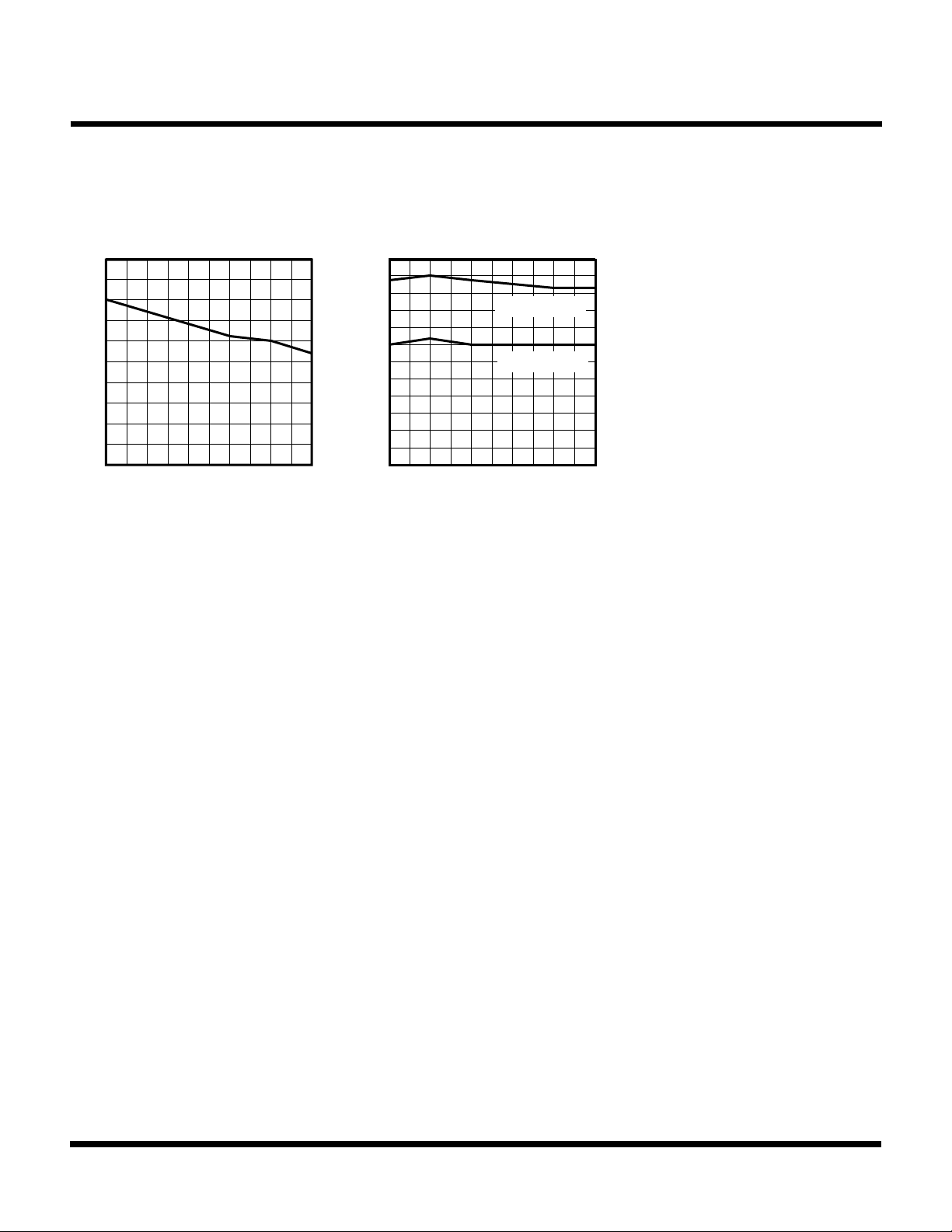
CONTROL VOLTAGE (ON)
1000
800
(mV)
600
400
CONT(ON)
V
200
0
-20 0 20 40 60 80
TEMPERATURE
TA (°C)
VS.
GROUND CURRENT VS.
300
250
200
(µA)
150
GND
I
100
50
0
-20 0 20 40 60 80
TEMPERATURE
I
OUT
I
OUT
TA (°C)
= 10 mA
= 5 mA
January 1999 TOKO, Inc. Page 5
Page 6
TK70403
DEFINITION AND EXPLANATION OF TECHNICAL TERMS
OUTPUT VOLTAGE (V
The output voltage is specified with VIN = V
and I
= 2 mA.
OUT
DROPOUT VOLTAGE (V
OUT
)
DROP
OUT(TYP)
+ 0.4
)
The dropout voltage is the difference between the input
voltage and the output voltage, at which point the regulator
starts to fall out of regulation. Below this value, the output
voltage will fall as the input value is reduced. It is dependent
upon the load current and the temperature.
OUTPUT CURRENT (I
OUT(MAX)
)
The rated output current is specified under the condition
where the output voltage drops 0.4 V when the output
current is loaded. The input voltage is set to V
OUT
+ 0.4 V.
LINE REGULATION (Line Reg)
Line regulation is the ability of the regulator to maintain a
constant output voltage as the input voltage changes. The
voltage is pulsed to minimize temperature effects.
LOAD REGULATION (Load Reg)
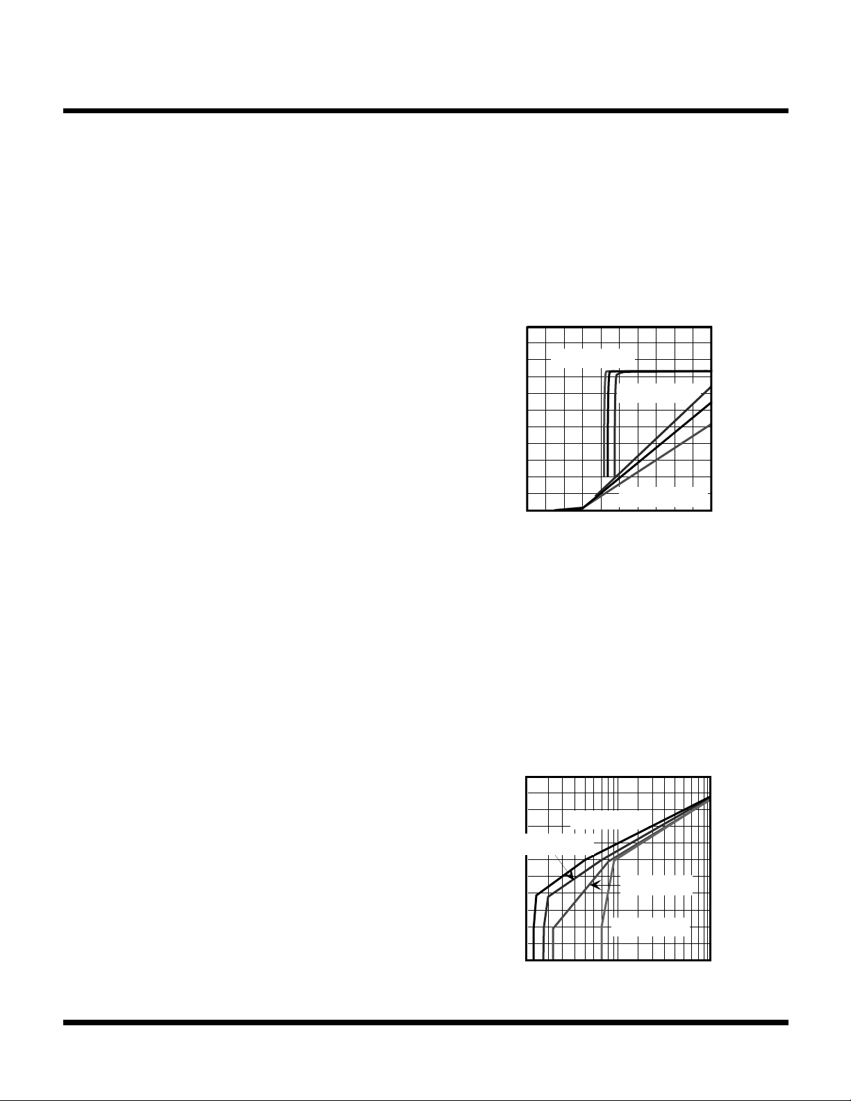
ON/OFF CONTROL
High is “on” (referenced to ground). When the on/off
function is not used, connect the control terminal to VIN.
The control current can be reduced by inserting a series
resistor (R
) between the control terminal and VIN.
CONT
Changes in the on/off level, due to this connection, are
shown below.
2
V
= 1 M
OUT
V
= 680 k
V
CONT
OUT
R
CONT
(V)
= 820 k
(µA)
1
CONT
I
0
0 1 2
ON/OFF RESPONSE WITH CONTROL (SPEED)
Load regulation is the ability of the regulator to maintain a
constant output voltage as the load current changes. It is
pulsed to minimize temperature effects. The load regulation
is specified to 0.1 mA to 5.0 mA.
QUIESCENT CURRENT (IQ)
The quiescent current is the current which flows through
the ground terminal under no load conditions (I
GROUND CURRENT (I
GND
)
OUT
= 0 mA).
Ground current is the current which flows through the
ground pin(s). It is defined as IIN - I
, excluding control
OUT
current.
RIPPLE REJECTION (RR)
Ripple rejection is the ability of the regulator to attenuate
the ripple content of the input voltage at the output. It is
specified with 50 mVp-p, 400 Hz, I
on the input voltage, where VIN = V
= 2 mA superimposed
OUT
OUT(TYP)
+ 0.4 V. The
ripple rejection is the ratio of the output vs. input and is
expressed in dB.
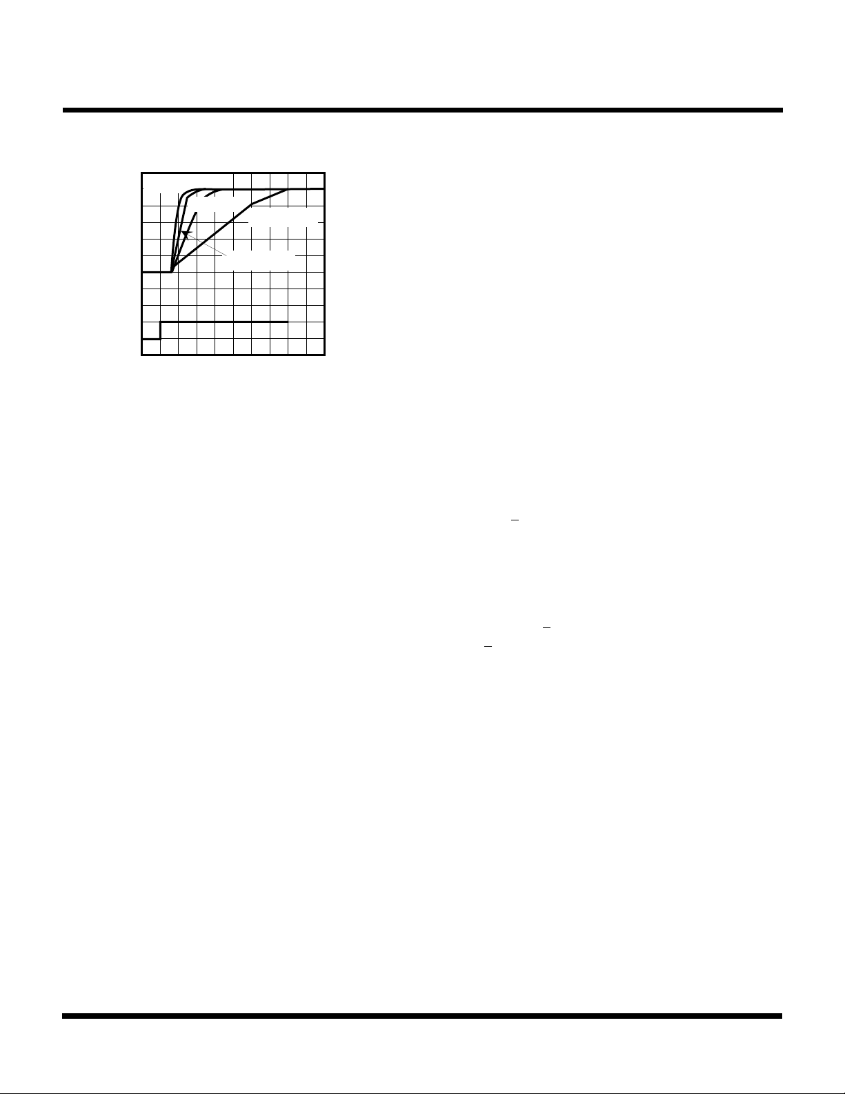
The turn-on time depends upon the value of the output
capacitor and the noise bypass capacitor. The turn-on time
will decrease with smaller value of either capacitor. The
graph below shows the relationship between turn-on time
and load capacitance. However, when the capacitance is
small, load transient and line transient will worsen and the
noise will increase. CL = 0.68 µF, CN = 1000 pF will be the
best for fastest operation.
.1 µ
.01 µ
N
1000 pF
C
100 pF
10 pF
CL = 0.68 µF
0
0 100 1000
CL = 0.45 µF
CL = 2.2 µF
CL = 4.7 µF
RISE TIME (µs)
Page 6 January 1999 TOKO, Inc.
Page 7
TK70403
DEFINITION AND EXPLANATION OF TECHNICAL TERMS (CONT.)
CL = 0.47 µF
CL = 2.2 µF
OUT
V
CONT
V
0 50
TIME (µs)
CL = 4.7 µF
CL = 0.68 µF
REDUCTION OF OUTPUT NOISE
Although the architecture of the Toko regulators is designed
to minimize semiconductor noise, further reduction can be
achieved by increasing the size of the output capacitor. A
more effective solution would be to add a capacitor to the
noise bypass terminal. The value of the capacitor should
be at least 0.1 µF or higher (higher values provide greater
noise reduction). Although stable operation is possible
without the noise bypass capacitor, this terminal has a high
impedance and care should be taken to avoid a large
circuit area on the printed circuit board when the capacitor
is not used. Please note that several parameters are
affected by the value of the capacitors and bench testing
is recommended when deviating from standard values.
thermal conductivity, the junction temperature will be low
even if the power dissipation is great. When mounted on
the recommended mounting pad, the power dissipation of
the SOT-26 is increased to 350 mW. For operation at
ambient temperatures over 25 °C, the power dissipation of
the SOT-26 device should be derated at 2.8 mW/°C. To
determine the power dissipation for shutdown when
mounted, attach the device on the actual PCB and
deliberately increase the output current (or raise the input
voltage) until the thermal protection circuit is activated.
Calculate the power dissipation of the device by subtracting
the output power from the input power. These
measurements should allow for the ambient temperature
of the PCB. The value obtained from PD /(150 °C - TA) is the
derating factor. The PCB mounting pad should provide
maximum thermal conductivity in order to maintain low
device temperatures. As a general rule, the lower the
temperature, the better the reliability of the device. The
thermal resistance when mounted is expressed as follows:
Tj = 0jA x PD + T
A
For Toko ICs, the internal limit for junction temperature is
150 °C. If the ambient temperature (TA) is 25 °C, then:
150 °C = 0jA x PD + 25 °C
0jA = 125 °C/ P
D
INPUT AND OUTPUT CAPACITORS
PD is the value when the thermal sensor is activated. A
simple way to determine PD is to calculate VIN x IIN when
Toko regulators require an output capacitor in order to
maintain regulator loop stability. The capacitor value should
be at least 0.68 µF over actual ambient operating
the output side is shorted. Input current gradually falls as
temperature rises. You should use the value when thermal
equilibrium is reached.
temperature.
PACKAGE POWER DISSIPATION (PD)
This is the power dissipation level at which the thermal
sensor is activated. The IC contains an internal thermal
sensor which monitors the junction temperature. When
the junction temperature exceeds the monitor threshold of
150 °C, the IC is shut down. The junction temperature
rises as the difference between the input power (VIN x IIN)
and the output power (V
OUT
x I
) increases. The rate of
OUT
temperature rise is greatly affected by the mounting pad
configuration on the PCB, the board material, and the
ambient temperature. When the IC mounting has good
January 1999 TOKO, Inc. Page 7
Page 8
TK70403
DEFINITION AND EXPLANATION OF TECHNICAL TERMS (CONT.)
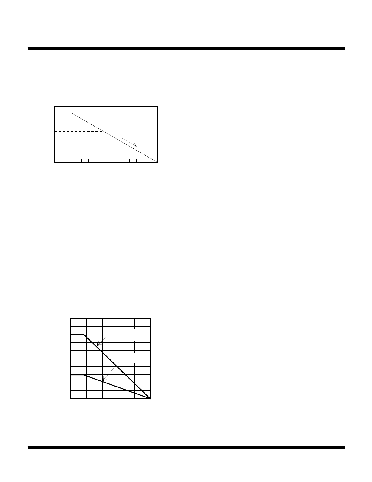
The range of usable currents can also be found from the
graph below.
(mW)
P
D
3
D
PD
6
4
5
25 50 75 150
TA (°C)
Procedure:
1) Find P
D
2) PD1 is taken to be PD x (~ 0.8 - 0.9)
3) Plot PD1 against 25 °C
4) Connect P
to the point corresponding to the 150 °C
D1
with a straight line.
5) In design, take a vertical line from the maximum
operating temperature (e.g., 75 °C) to the derating
curve.
6) Read off the value of PD against the point at which the
vertical line intersects the derating curve. This is taken
as the maximum power dissipation, DPD.
The maximum operating current is:
I
OUT
(mW)
D
P
= (D
450
350
250
150
50
/ (V
PD
IN(MAX) - VOUT
0
0 50 100 150
TA (°C)
)
MOUNTED AS
SHOWN
FREE AIR
SOT-26 POWER DISSIPATION CURVE
Page 8 January 1999 TOKO, Inc.
Page 9
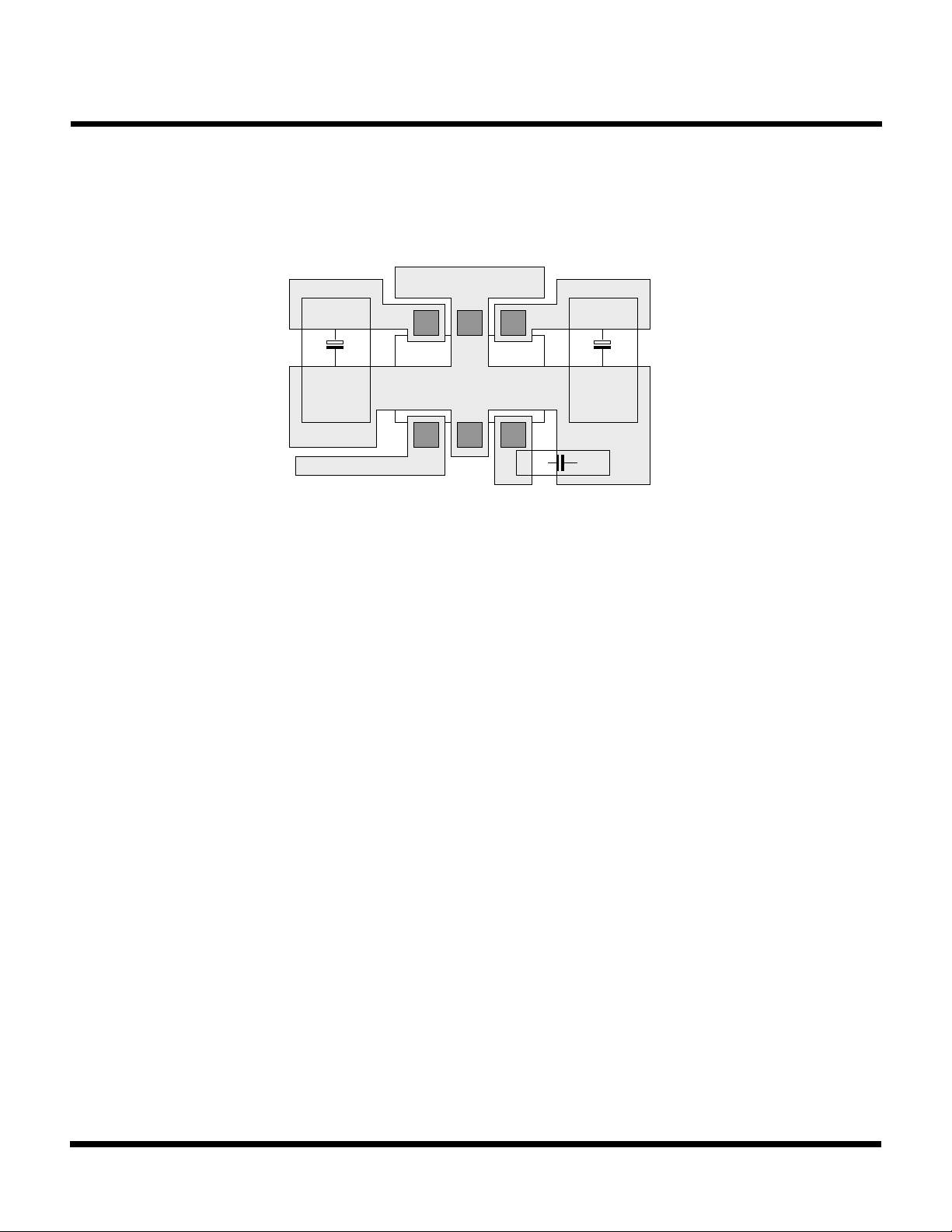
BOARD LAYOUT
TK70403
APPLICATION INFORMATION
V
IN
CONTROL
GND
SOT-26 BOARD LAYOUT
V
++
OUT
January 1999 TOKO, Inc. Page 9
Page 10
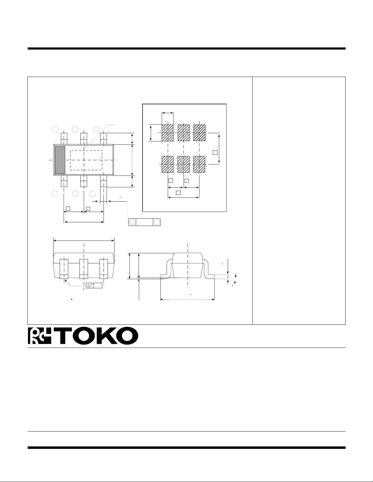
TK70403
)
PACKAGE OUTLINE
SOT-26 (SOT-23-6)
6
1
5
2
3
(1.9)
0.950.95
e
2.9
e
Marking Information
0.7
4
Marking
0.3
1.0
(0.6)
2.4
1
e
1.6
e
(0.6)
+
0.1
Recommended Mount Pad
M
0.1
1.1
1.4 max
0.95
e
0.95
e
1.90
0.1
+
0.15
Marking
TK70403 03J
0.1
Dimensions are shown in millimeters
Tolerance: x.x = 0.2 mm (unless otherwise specified
0 ~ 0.1
+
0.3
2.8
0-13
Toko America, Inc. Headquarters
1250 Feehanville Drive, Mount Prospect, Illinois 60056
Tel: (847) 297-0070 Fax: (847) 699-7864
TOKO AMERICA REGIONAL OFFICES
Midwest Regional Office
Toko America, Inc.
1250 Feehanville Drive
Mount Prospect, IL 60056
Tel: (847) 297-0070
Fax: (847) 699-7864
Western Regional Office
Toko America, Inc.
2480 North First Street , Suite 260
San Jose, CA 95131
Tel: (408) 432-8281
Fax: (408) 943-9790
Eastern Regional Office
Toko America, Inc.
107 Mill Plain Road
Danbury, CT 06811
Tel: (203) 748-6871
Fax: (203) 797-1223
Semiconductor Technical Support
Toko Design Center
4755 Forge Road
Colorado Springs, CO 80907
Tel: (719) 528-2200
Fax: (719) 528-2375
Visit our Internet site at http://www.tokoam.com
The information furnished by TOKO, Inc. is believed to be accurate and reliable. However, TOKO reserves the right to make changes or improvements in the design, specification or manufacture of its
products without further notice. TOKO does not assume any liability arising from the application or use of any product or circuit described herein, nor for any infringements of patents or other rights of
third parties which may result from the use of its products. No license is granted by implication or otherwise under any patent or patent rights of TOKO, Inc.
Page 10 January 1999 TOKO, Inc.
All Rights Reserved
IC-216-TK70001
0798O0.0K
Printed in the USA© 1999 Toko, Inc.
 Loading...