

Page 1
TISPPBL2SD
‡ C
SLIC inf
K1
PROGRAMMABLE OVERVOLTAGE PROTECTORS
FOR ERICSSON COMPONENTS PBL 3xxx SLICS
AUGUST 1999Copyright © 1999, Power Innovations Limited, UK
OVERVOLTAGE PROTECTION FOR ERICSSON COMPONENTS LINE INTERFACE CIRCUITS
Overvoltage Protector‡ for:-
●
PBL 3762A
PBL 3764A/4, PBL 3764A/6
PBL 3766, PBL 3766/6
PBL 3767, PBL 3767/6
PBL 3796, PBL 3796/2
PBL 3798, PBL 3798/2
PBL 3798/5
PBL 3798/6
PBL 3799
PBL 3860A/1, PBL 3860A/6
PBL 386 10/2
PBL 386 11/2
PBL 386 20/1
PBL 386 21/1
PBL 386 30/1
PBL 386 40/1
PBL 386 50/1
PBL 3898/M
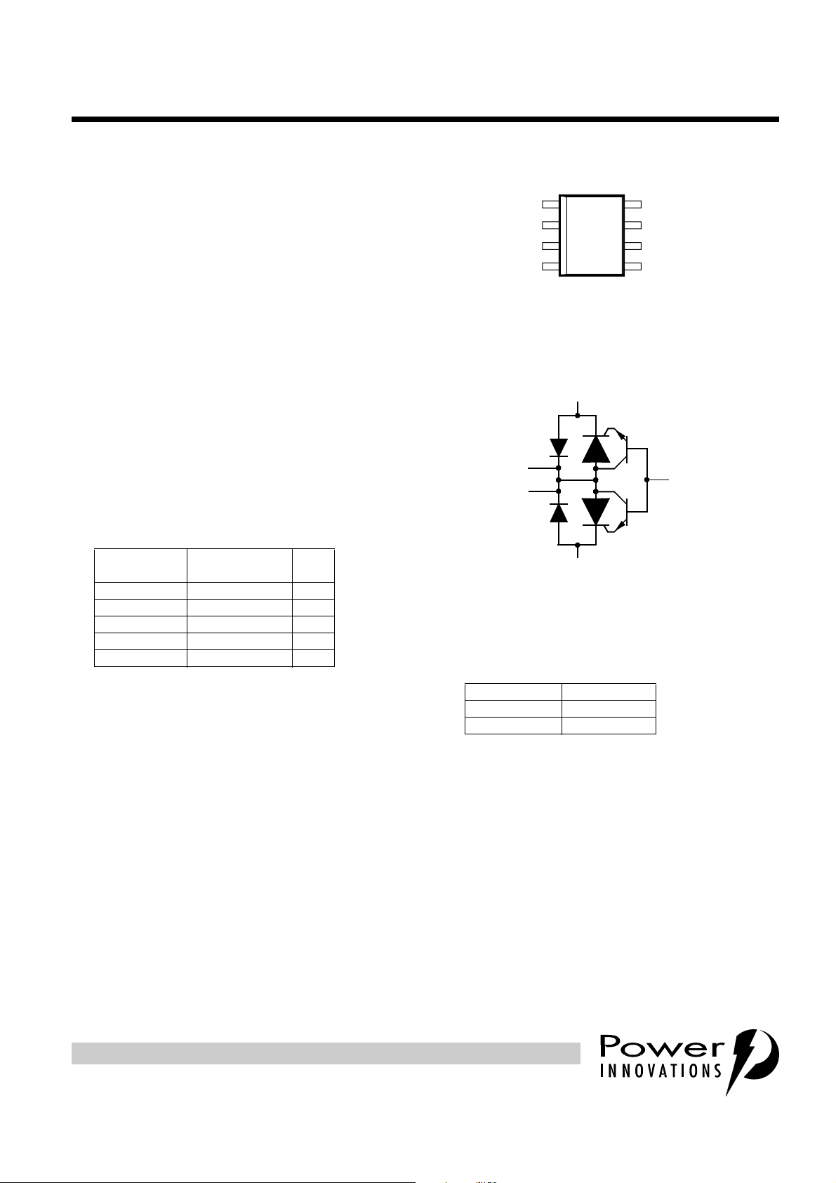
(Tip)
(Gate)
(Ring)
Terminal typical application names shown in
device symbol
A
A
D PACKAGE
(TOP VIEW)
K1
G
NC
K2
NC - No internal connection
1
2
3
4
parenthesis
8
7
6
5
NC
A
A
NC
(Ground)
(Ground)
MD6XBA
G1,G2
Rated for International Surge Wave Shapes
●
I
WAVE SHAPE STANDARD
2/10 µs GR-1089-CORE 100
1.2/50 µs ITU-T K22 100
0.5/700 µs I3124 40
10/700 µs ITU-T K20, K21 40
10/1000 µs GR-1089-CORE 30
Single-Lead Line Connection Version of
●
Feed-Through TISPPBL2D
- Ground Lead Creepage Distance . . > 3 mm
TSP
A
K2
Termin als K1, K2 and A cor respond to t he alternative
line designators of T, R and G or A, B and C. The
negative protection voltage is controlled by the
voltage, V
Small Outline Surface Mount Package
●
applied to the G terminal.
GG,
- Available Ordering Options
CARRIER ORDER #
Tube TISPPBL2SD
Taped and reeled TISPPBL2SDR
description
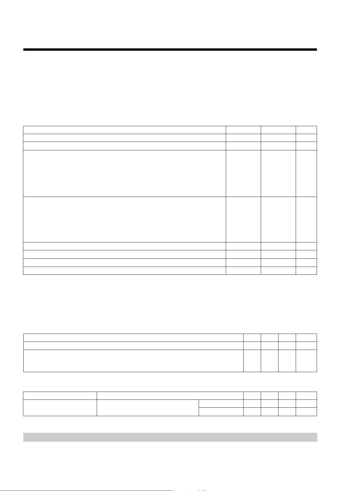
The TISPPBL2S is a dual forward-conducting buffered p-gate overvoltage protector. It is designed to p rotect
the Ericsson Components PBL 3xxx family of SLICs (Subscriber Line Interface Circuits) against overvoltages
on the telephone line cause d by lightning, a.c. power contact and indu ction. The TISPPB L2S limits voltages
that exceed the SLIC supply rail levels.
The SLIC line driver section is typically powered from 0 V (ground) and a negative voltage in the region of
-10 V to -85 V. The protector gate is connected to this negative supply. This references the protection
(clipping) voltage to the negative supply voltage. As the protection voltage will track the negative supply
voltage the overvoltage stress on the SLIC is minimised.
SD6XAP
Positive overvoltage s are clipped to grou nd by diode forward conduction. Negative overvoltage s are initially
clipped close to the SLIC negative supply rail value. If sufficient current is available from the overvoltage, then
the protector will crowbar into a low voltage ground referenced on-state condition. As the overvoltage
ustomers are advised to obtain the latest version of the relevant Ericsson Components
the information being relied on is current.
ormation to verify, before placing orders, that
PRODUCT INFORMATION
Information is current as of publication date. Products conform to specifications in accordance
with the terms of Power Innovations standard warranty. Production processing does not
necessarily include testing of all parameters.
1
Page 2
TISPPBL2SD
PROGRAMMABLE OVERVOLTAGE PROTECTORS
FOR ERICSSON COMPONENTS PBL 3xxx SLICS
AUGUST 1999
subsides the high holdin g c ur rent of th e cr owbar prevents d.c. latchup. The TISPPBL2S buffered gate design
reduces the loading on the SLIC supply during overvoltages caused by power cross and induction.
These monolithic prote ction devices are fabricated in ion-implanted planar vertical power str uctures for high
reliability and in nor mal system operatio n they are virtual ly transparent. The TISPPBL2 S is the TISPPBL2D
with a different pinout. The feed-through Ring ( leads 4 — 5) and Tip (lead s 1 — 8) connections have been
replaced by single Ring (lea d 4) and Tip ( lead 1) connec tions. This in creases pa ckage creepag e distance of
the biased to ground connections from about 0.7 mm to over 3 mm.
absolute maximum ratings
RATING SYMBOL VALUE UNIT
≤
Repetitive peak off-state voltage, I
Repetitive peak gate-cathode voltage, V
Non-repetitive peak on-state pulse current (see Notes 1 and 2)
10/1000 µs (Bellcore GR-1089-CORE, Issue 1, November 1994, Section 4) 30
0.2/310 µs (I3124, open-circuit voltage wave shape 0.5/700µs)
5/310 µs (ITU-T K20 & K21, open-circuit voltage wave shape 10/700 µs)
1/20 µs (ITU-T K22, open-circuit voltage wave shape 1.2/50 µs)
2/10 µs (Bellcore GR-1089-CORE, Issue 1, November 1994, Section 4) 100
Non-repetitive peak on-state current, 50/60 Hz (see Notes 1 and 2)
100 ms 11
1s
5s
300 s
900 s
Non-repetitive peak gate current, 1/2 µs pulse, cathodes commoned (see Note 1) I
Operating free-air temperature range T
Junction temperature T
Storage temperature range T
= 0, -40°C≤T
G
= 0, -40°C≤T
KA
85°C V
J
≤
85°C V
J
DRM
GKRM
I
TSP
I
TSM
GSM
A
J
stg
-100 V
-90 V
40
40
100
4.5
2.4
0.95
0.93
40 A
-40 to +85 °C
-40 to +150 °C
-40 to +150 °C
A
A
NOTES: 1. Initially the protector must be in thermal equilibrium with -40 °C≤T
its initial conditions.
2. These non-repetitive rated currents are peak values for either polarirty. The rated current values may be applied either to the Ring
to Ground or to the Tip to Ground terminal pairs. Additionally, both terminal pairs may have their rated current values applied
simultaneously (in this case the Ground terminal current will be twice the rated current value of an individual terminal pair). Above
85 °C, derate linearly to zero at 150 °C lead temperature.
recommended operating conditions
C
G
R
1
electrical characteristics, T
I
D
Gate decoupling capacitor 100 220 nF
TISPPBL2S series resistor for GR-1089-CORE first-level and second-level surge survival
TISPPBL2S series resistor for GR-1089-CORE first-level surge sur vival
TISPPBL2S series resistor for ITU-T recommendation K20/21
= 25 °C (unless otherwise noted)
amb
PARAMETER TEST CONDITIONS MIN TYP MAX UNIT
Off-state current VD=V
DRM
, VGK=0
PRODUCT INFORMATION
≤
85 °C. The surge may be repeated after the device returns to
J
MIN TYP MAX UNIT
40
25
10
T
= -40 °C -5 µA
J
= 85 °C -50 µA
T
J
Ω
2
Page 3
TISPPBL2SD
PROGRAMMABLE OVERVOLTAGE PROTECTORS
FOR ERICSSON COMPONENTS PBL 3xxx SLICS
AUGUST 1999
electrical characterist ics, T
PARAMETER TEST CONDITIONS MIN TYP MAX UNIT
I
V
t
(BR)
V
V
t
FR
I
H
I
GAS
I
GAT
I
GAF
I
GT
V
C
(BO)
F
FRM
GT
AK
Breakover voltage
Breakdown time
Forward voltage IF= 5 A, tw= 500 µs 3V
Peak forward recovery
voltage
Forward recovery time
Holding current IT= -1 A, di/dt = 1A/ms, VGG=-50V, -40°C≤T
Gate reverse current VGG=V
Gate reverse current,
on state
Gate reverse current,
forward conducting
state
Gate trigger current IT=-5A, t
Gate trigger voltage IT=-5A, t
Anode-cathode offstate capacitance
T
Figure 2)
I
T
cuit (See Note 3 and Figure 2)
IF= 20 A, 0.5/700 generator, Fi gure 3 test circuit (See Note 4 and Figure 2)
I
F
cuit (See Note 4 and Figure 2)
I
T
I
F
f=1MHz, V
= 25 °C (unless otherwise noted) (continued)
amb
= -20 A, 0.5/700 generator, Figure 3 test circuit (See Note 3 and
= -20 A, 0.5/700 generator, Figure 3 test cir-
< -50 V 1 µs
V
(BR)
-70 V
8V
10000
1
µs
= 20 A, 0.5/700 generator, Figure 3 test cir-
, VAK=0
GKRM
VF > 5 V
> 1 V
V
F
≤
85 °C -150 mA
J
T
= -40 °C -5 µA
J
T
= 85 °C -50 µA
J
=-0.5A, tw= 500 µs, VGG=-50V -1 mA
= 1 A, tw= 500 µs, VGG= -50 V -10 mA
≥
20 µs, V
p(g)
≥
20 µs, V
p(g)
=1V, IG= 0, (see Note 5)
d
=-50V 5 mA
GG
=-50V 2.5 V
GG
V
= -3 V 110 pF
D
V
=-50V 60 pF
D
NOTES: 3. For the required TIPX and RINGX terminal negative pulse performance refer to the respective Ericsson Components SLIC data
sheet. The PBL 379x family of SLICs has ratings of -120 V for 0.25 µs, -90 V for 1 µs, -70 V for 10 ms and -70 V for d.c. The PBL
376x family together with the PBL 3860A SLIC have the same maximum ratings when the applied battery voltage is -50V. As the
FLEXI-SLIC™ PBL 386 xx family is specified in terms of current pulses, a minimum value of 2Ω for R
Compliance to these conditions is guaranteed by the maximum breakover voltage and the breakdown times of the TISPPBL2S.
should be used.
P
4. For the required TIPX and RINGX terminal positive pulse performance refer to the respective Ericsson Components SLIC data
sheet. The PBL 379x family of SLICs has ratings of 15 V for 0.25 µs, 10 V for 1µs, 5 V for 10 ms and 1 V for d.c. The PBL 376x
family together with the PBL 3860A SLIC have similar ratings. As the FLEXI-SLIC™ PBL 386 xx family is specified in terms of
current pulses, a minimum value of 2Ω for R
should be used. Compliance to these conditions is guaranteed by the peak forward
P
recovery voltage and the forward recov ery times of the TISPPBL2S
5. These capacitance measurements employ a three terminal capacitance bridge incorporating a guard circuit. The unmeasured
device terminals are a.c. connected to the guard terminal of the bridge.
thermal characteristics
PARAMETER TEST CONDITIONS MIN TYP MAX UNIT
P
=0.8W, TA=25°C
R
Junction to free air thermal resistance
θ
JA
tot
5cm
2
, FR4 PCB
D Package 160 °C/W
PRODUCT INFORMATION
3
Page 4
TISPPBL2SD
PROGRAMMABLE OVERVOLTAGE PROTECTORS
FOR ERICSSON COMPONENTS PBL 3xxx SLICS
AUGUST 1999
PARAMETER MEASUREMENT INFORMATION
V
GK(BO)
-v
I
(BO )
V
V
(BO)
Quad r a nt III
Switchin g
Characteristic
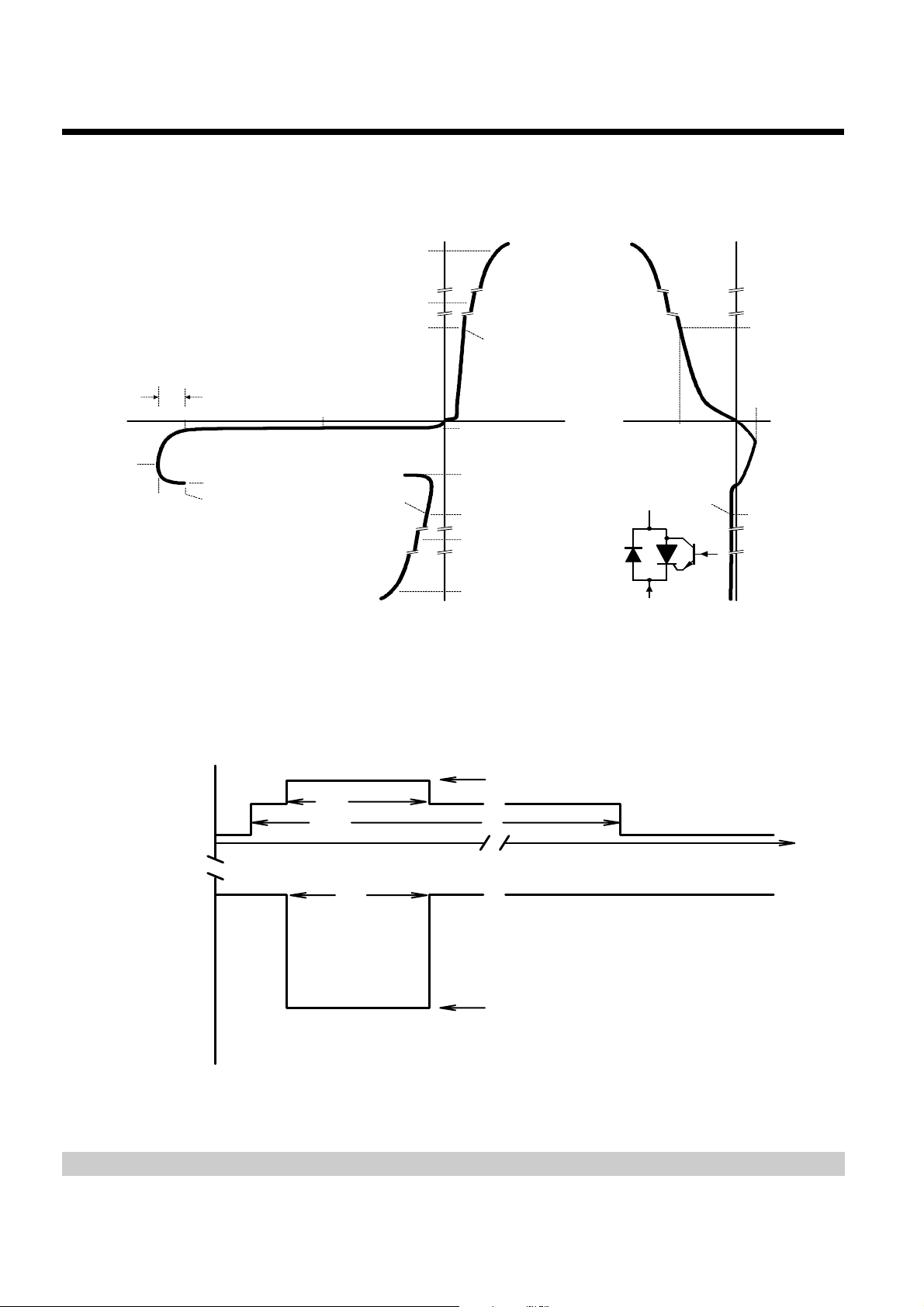
Figure 1. PRINCIPAL TERMINAL AND GATE TRANSFER CHARACTERISTICS
PRINCIPAL TERMINAL V-I CHARACTERISTIC
(= |I
I
FSP
I
(= |I
FSM
TSM
GG
I
S
V
S
V
D
V
T
TSP
GATE TRANSFER
CHARACTERISTIC
+i
|)
Quadrant I
Forward
Conduction
Characteristic
+i
K
|)
I
F
V
F
+v
-i
PM6XAIA
G
I
GAF
I
GAT
I
K
I
D
I
H
I
T
I
TSM
I
TSP
-i
I
F
I
GT
+i
G
I
T
I
G
-i
K
PROTECTOR MAXIMUM LIMIT ING VOLTAGE
vs
TIME
-50
VOLTAGE - V
-60
-70
-80
10
5
1 µs
10 ms
0
1 µs
MAX V
MAX V
FRM
(BO)
= 8 V
= -70 V
Figure 2. TRANSIENT LIMITS FOR TISPPBL2S LIMITING VOLTAGE
V
BAT
Time
= -50 V
PM6XAL
PRODUCT INFORMATION
4
Page 5
TISPPBL2SD
E502 0.5/700 WAVEFRONT di/dt
vs
TIME
Time - µs
0.0 0.1 0.2 0.3 0.4 0.5 0.6 0.7 0.8 0.9 1.0
di/dt - Rate of Rise of Wavefront Current - A/µs
0
10
20
30
40
50
60
70
80
AI6XAZ
PROGRAMMABLE OVERVOLTAGE PROTECTORS
FOR ERICSSON COMPONENTS PBL 3xxx SLICS
AUGUST 1999
IMPULSE
R1
CURRENT
ΩΩΩΩ
50
Hi
I
, I
T
F
S1
±1960 V
ECAT WITH E502 0.5/700 SURGE NETWORK
R1 = ONE SECTION OF A PBR 530 01/1 LPC LINE
RESISTOR NETWORK
Figure 3. TEST CIRCUIT FOR MEASUREMENT OF LIMITING VOLTAGE
E502 0.5/700 WAVEFRONT CURRENT
vs
TIME
20
15
10
15
25
ΩΩΩΩ
20 nF20 µF
AI6XAY
ΩΩΩΩ
VOLTAGE
Lo
LIMITING
, V
V
K
F
220 nF
Th4
Th5
DUT
(TISPPBL2S)
V
I
GG
G
-50 V
(V
)
BAT
AI6XBAS
i - Wavefront Current - A
5
0
0.0 0.2 0.4 0.6 0.8 1.0 1.2 1.4 1.6 1.8 2.0
Time - µs
Figure 4. CURRENT WAVEFRONT Figure 5. CURRENT WAVEFRONT di/dt
PRODUCT INFORMATION
5
Page 6

TISPPBL2SD
PROGRAMMABLE OVERVOLTAGE PROTECTORS
FOR ERICSSON COMPONENTS PBL 3xxx SLICS
AUGUST 1999
THERMAL INFORMATION
PEAK NON-RECURRING A.C.
vs
CURRENT DURATION
10
RING AND TIP CONNECTIONS Equal I
GROUND CONNECTION Curren t is twice I
values were applied to both
TSM
TSM
V
GEN
R
GEN
VG = -48 V, T
value
= 600 Vrms
= 70 to 950
AMB
TI6LACA
Ω
Ω
Ω Ω
= 85°C
- Peak Non-Recurrent 50 Hz Current - A
TSM
1
I
0·1 1 10 100 1000
t - Current Duration - s
Figure 6.
PRODUCT INFORMATION
6
Page 7

0
DISTRIBUTION LIMITS OF
DIODE FORWARD VOLTAGE
vs
TIME
Time - µs
0.0 0.1 0.2 0.3 0.4 0.5 0.6 0.7 0.8 0.9 1.0
V
F
- Forward Voltage - V
0
1
2
3
4
5
6
AI6XAX
50 devices tested from 10 wafer lots
0.5/700 Waveform
I
F
= 20 A
T
A
= 25°C
V
GG
= -50 V
TC61AD
DIODE FORWARD CURRENT
vs
FORWARD VOLTA G E
VF - Forward Voltage - V
0.5 0.6 0.7 0. 8 0.9 1.0 1.1 1.2
I
F
- Forward Current - A
0.02
0.04
0.07
0.2
0.4
0.7
0.01
0.1
1
-40°C25°C
85°C
-10
-20
-30
-40
- Cathode Voltage - V
K
-50
V
TYPICAL CHARACTERISTICS
DISTRIBUTION LIMITS OF
THYRISTOR LIMITING VOLTAGE
vs
TIME
50 devices tested from 10 wafer lots
0.5/700 Waveform
= -20 A
I
T
= 25°C
T
A
= -50 V
V
GG
TISPPBL2SD
PROGRAMMABLE OVERVOLTAGE PROTECTORS
FOR ERICSSON COMPONENTS PBL 3xxx SLICS
AUGUST 1999
AI6XAW
-60
-70
0.0 0.1 0.2 0.3 0.4 0.5 0.6 0.7 0.8 0.9 1.0
CUMULATIVE POPULATION %
PEAK LIMITING VOLTAGE
99·999
99·99
0·001
50 devices tested from 10 wafer lots
I
= 20 A, IT = -20 A, 0.5/700 Waveform
F
99·9
Cumulative Populati on - %
0·01
= 25°C, VGG = -50 V
T
A
99
90
70
50
30
10
1
0·1
456789 1510
DIODE
V
FRM
Time - µs
Figure 7. Figure 8.
vs
TC6XAB
THYRISTOR
- V
V
GG
(BO)
Peak Limiting Voltage - V
Figure 9. Figure 10.
PRODUCT INFORMATION
7
Page 8

TISPPBL2SD
PROGRAMMABLE OVERVOLTAGE PROTECTORS
FOR ERICSSON COMPONENTS PBL 3xxx SLICS
AUGUST 1999
CUMULATIVE POPULATION %
vs
LIMITING TIME
99·999
50 devices tested from 10 wafer lots
99·99
I
= 20 A, IT = -20 A, 0.5/700 Waveform
F
99·9
= 25°C, VGG = -50 V
T
A
99
90
70
50
30
10
1
DIODE t
FR
for VF > 5 V
Outliers
(2) @ 0 µs
THYRISTOR t
for V
(BR)
Cumulative Population - %
0·1
0·01
0·001
0.001 0.01 0.1 1
t
(BR)
0.004 0.04 0.4
, tFR - Breakdown and Forward Recovery Times - µs
Figure 11. Figure 12.
< V
TC6XAC
(BR)
GG
NORMALISED PEAK LIMITING VOLTAGES
vs
JUNCTION TEMPERATURE
1.10
Normalised to 25°C values
and V
of V
(BO)
IF = 20 A, IT = -20 A
0.5/700 Waveform
1.05
V
GG
= -50 V
THYRISTOR
1.00
0.95
DIODE
0.90
-40-30-20-100 1020304050607080
FRM
V
(BO)
V
FRM
TJ - Junction Temperature - °C
TC6XAA
APPLICATIONS INFORMATION
operation of gated protectors
Figure 13 and Figure 14 show how the TISPPB L2S limits overvoltages. The TISPPBL2S thyristor section s
limit negative overvoltages and the diode sections limit positive overvoltages.
SLIC
PROTECTOR
SLIC
I
K
AI6XANS
V
PBL2S
GG
TISP
Th5
C1
I
G
V
Bat
D1
C2
I
F
AI6XAOS
Figure 13. NEGATIVE OVERVOLTAGE CONDITION Figure 14. POSITIVE OVERVOLTAGE CONDITION
Negative overvoltages (Figure 13) are initially cl ipped close to the SLIC ne gative supply rail value (V
the conduction of t he transistor base-emi tter and the thyristor g ate-cathode junctio ns. If sufficient curren t is
SLIC
PROTECTOR
Th5
TISP
PBL2S
V
C1
GG
D1
SLIC
V
C2
Bat
) by
BAT
PRODUCT INFORMATION
8
Page 9

TISPPBL2SD
PROGRAMMABLE OVERVOLTAGE PROTECTORS
FOR ERICSSON COMPONENTS PBL 3xxx SLICS
AUGUST 1999
available from the overvoltage, then the thyristor will crowbar into a low voltage ground referenced on-state
condition. As the overvoltage subsides the high holding current of the crowbar thyristor prevents d.c. latchup.
The negative protection voltage will be the sum of the gate supply (V
voltage (V
). Under a.c. overvoltage conditions V
GK(BO)
will be less than 3 V. The integrated transistor
GK(BO)
) and the peak gate(terminal)-cathode
BAT
buffer in the TISPPBL2S greatly reduces protectors source and sink current loading on the V
Without the transistor, the thyristor gate current would charge the V
supply. An electronic power supply is
BAT
not usually designed to b e charged like a batter y. As a result , the electronic supp ly would switch off and the
thyristor gate current would provide the SL IC supply current. Nor mally the SLIC current wou ld be less than
the gate current, which would cause the supply voltage to increase and destroy the SLIC by a supply
overvoltage. The integrated transistor buffer removes this problem.
Fast rising impulses will cause short term overshoots in gate-cathode voltage. The negative protection
voltage under impulse conditions will also be increased if there is a long connection between the gate
decoupling capacitor, C1, and the gate terminal. During the initial rise of a fast impulse, the gate current (I
the same as the cathode current (I
). Rates of 60 A/µs can cause inductive voltages of 0.6 V in 2.5 cm o f
K
printed wiring track. To minimise this inductive voltage increase of protection voltage, the length of the
capacitor to gate ter minal tracking should be minimised. Inductive voltages in the protec tor cathode wiring
can increase the protection voltage. These voltages can be minimised by routing the SLIC connection via the
protector as shown in Figure 13 and Figure 14.
Positive overvoltages (Figure 14) are clipped to ground by forward conduction of the diode section in the
TISPPBL2S. Fast rising impulses will cause short term overshoots in forward voltage (V
FRM
).
TISPPBL2S limiting voltages
This clause details the TISPPBL2S voltage limiting levels under impulse conditions.
test circuit
Figure 3 shows the basic test circuit used for the measurement of impulse limiting voltage. During the
impulse, the high levels of electrical en er gy and rapid rates of change cause electrical noise to be i ndu ce d or
conducted into the me asurement system. It i s possible for the electrical nois e voltage to be many times the
wanted signal voltage. Elaborate wiring and measurement techniques where used to reduce the noise
voltage to less than 2 V peak to peak.
BAT
supply.
) is
G
impulse generator
A Keytek ECAT E-Class series 100 wi th an E 502 surge networ k was used for testing. The E 502 pro duces a
0.5/700 voltage impulse. This particular waveform was used as it ha s the fastest rate of curren t r ise (di/dt) o f
the commonly used lightning surge waveforms. This maximises the measured limiting voltage. Figure 4
shows the current wavefront through the DUT. To produce a peak test current level of ±20 A, the E502
charging voltage was set to ±1960 V. Figure 5 shows the DUT current di/dt. Initially the wavefront current rises
at 60 A/µs, this rate then reduces as the peak current is approached. At the TISPPBL2S V
condition the
(BO)
di/dt is about 50 A/µs.
limiting voltage levels
Fifty devices were measured in the test circ uit of Figure 3. The 50 devices were made up from groups of 5
devices taken from 10 separately processed device lots. Figure 7 shows the total waveform variation of the
thyristor limiting voltage acr oss the 50 devices. This shows t hat the largest peak limiting voltage (Bre akover
volt a ge, V
exceeds the gate reference supply voltage level for a period (t
) is -62 V, a 12 V overshoot beyond the -50 V gate reference supply, VGG. The limiting voltage
(BO)
) of about 0.4 µs.
(BR)
PRODUCT INFORMATION
9
Page 10

TISPPBL2SD
PROGRAMMABLE OVERVOLTAGE PROTECTORS
FOR ERICSSON COMPONENTS PBL 3xxx SLICS
AUGUST 1999
Figure 9 and Figure 11 s how these two waveform parameters in ter ms of device pop ulation. In Fig ure 9, the
limiting voltage is shown in terms of the overshoot bey ond the gate reference supply (V
the gate reference voltage level magnifies the thyristor limiting voltage variation and shows the data
stratification caused by the osci ll os co pe di git isati on. Ex trapolating the data tren d ind ic ate s that th e overshoot
is less than 14 V at the 99.9 97% level (equal to 30 ppm of the populatio n exceeding 14 V, equivalent to +4
sigma point of a nor mal distr ibution). In Figure 11, extrapolating the thyristor data trend to the 99.997 % level
indicates a maximum breakdown time, t
, of 0.5 µs. Figure 12 shows that inc reasing the temperature up to
(BR)
85°C increase s the thyristor p eak limiting voltage by 2.4%, giving a maximum 85° C peak limiting voltage of
1.024x(-50-14) = -65.5 . Over the -40°C to 85°C temperature range the TISPPBL2S is sp ecified to have a
maximum V
value of -70 V and a breakdown time, t
(BO)
(BR)
, of 1 µs.
Figure 8 shows the total waveform variation of the d iode limiting voltage across the 50 devices. The peak
limiting voltage (Peak Forward Recovery Voltage V
) is less than 6 V, and this value includes the 2 V of
FRM
magnetically indu ced noise in the probe. Figure 9 shows that extrapolated 99.997% level is about 5.5 V. In
Figure 11, extrapolating the diode da ta trend to the 99.997% level indicates a maximum forward recovery
time, t
, of 0.1 µs. Figure 12 indicates that there is about a 10% uplift by increasing the temperature to 85°C.
FR
This gives a maximum 85°C peak limitin g voltage of 1.1x(5.5) = 6.1 V. Over the -40°C to 85°C temperature
range, the TISPPBL2S is specified to have a maximum V
value of 8 V and a maximum forward recovery
FRM
time of 1 µs.
GG
- V
(BO)
). Removing
Diodes do not switch to a much lower voltage like thyristors, so the diode limiting voltage applies for the whole
impulse duration. Forward voltages of 1 V or less are nor mally considered safe. Figure 10 shows that the
lowest current 1 V condition occurs a t -40°C with a c urrent of 0.3 A. Wh en the TIS PPBL 2S is tes ted w ith the
rated 10/1000 impulse it would take about 8 ms for the current to decay from 30 A to 0.3 A. Over the -40°C to
85°C temperature range, the TISPPBL2S is specified to have a V
below 1 V within 10 ms.
F
SLIC protection requirements
This clause discusses the various requirements of the Ericsson Components SLICs detailed on the first page
of this data sheet and co mpares these to the TISPPBL2 S protector parameters. Some SLICs are rated for
0°C to 70°C operation, others for -40°C to 85°C operation. The TISPPBL2S protector is specified for -40°C to
85°C operation and so covers both temperature ranges.
normal operation
Depending on the SLIC type, the maximum SLIC supply voltage rating (V
-85V rating of the TISPPBL2S gate-cathode (V
) matches the highest SLIC voltage rating.
GKRM
To restore normal op eration after the TISP PBL2S has switched on, the minimum switch-off curr ent (holding
current I
) needed is equal to the maximum SL IC short circuit current to ground (d.c. line current together
H
with the maximum longitudinal current). For the SLICs listed on the first page of this data sheet, the
TISPPBL2S minimum holding current of 140 mA will ensure switch-off after an overvoltage.
overvoltage protection
Ericsson Com ponents specify SL IC withstand capabi lity as a serie s of stress-tim e values. Figure 15 shows
the voltage withstand limits of the PBL 3762A SLIC.
) will be -70 V, -80 V or -85 V. The
Bat
In the positive polar ity, the PBL 3762A RING or TIP voltage must not exceed +1 5 V. For 250 ns, the PBL
3762A will be able to w ithstand a voltage between +1 0 V and +15 V. For 1 µs, the PBL 379 6 will be able to
withstand a voltage between +5 V and +10 V. For 10 ms, the PBL 3796 will be able to withstand a voltage
between +2 V and +5 V. To protect against positive overvoltage, the TISPPBL2S positive limiting voltage must
be equal to or less than these voltage values during the specified time periods.
PRODUCT INFORMATION
10
Page 11

TISPPBL2SD
PROGRAMMABLE OVERVOLTAGE PROTECTORS
FOR ERICSSON COMPONENTS PBL 3xxx SLICS
AUGUST 1999
PBL 3762A SLIC RING AND TIP VOLTAGE WITHSTAND
vs
- 70 V
V
BAT
TIME
- 40 V
Time
V
BAT
V
- 20 V
BAT
D.C. and 10 ms pulse rating increased
to -70 V (independent of V
by use of series battery feed diode
value)
BAT
AI6XBC
15
10
5
0
set to -50 V) - V
-50
BAT
-60
-70
-80
-90
Voltages (with V
-100
-110
-120
0.25 µs
1 µs
10 ms
10 ms
1 µs
0.25 µs
V
BAT
Figure 15. TRANSIENT LIMITS FOR PBL 3762A WITHSTAND VOLTAGE
In the negative polarity, the PBL 3762 A RING or TIP voltage must not exceed V
PBL 3762A can withstand a V
drawn for a V
of -50 V and so that the peak voltage becomes -120 V.
BAT
For 250 ns, the PBL 3762A will be able to withst and a voltage between V
of -70 V and this implies a maximum peak voltage of -140 V. Figure 15 is
BAT
-40V and V
BAT
and -120 V in this case. For 1 µs, the PBL 3796 will be a ble to withstand a voltage between V
V
-40 V or -70 V and -90 V in this case. For 10 ms, the PBL 379 6 will be able to withstand a voltage
BAT
between V
BAT
and V
-20 V o r -50 V and -70 V in this case. By adding a ser ies feed diode in the battery
BAT
feed the d.c. and 10 ms voltage withstands increase to -70 V, independent of the actual V
- 70. Continuously the
BAT
-70V or -90V
BAT
BAT
-20V and
BAT
valu e.To protect
against negative overvoltage, the TISP PBL2S negative limitin g voltage must be equal t o or less than thes e
voltage values during the specified time periods.
The following table lists the protection requiremen ts of three sel ections from different SLIC families. Two, the
PBL 3796 and the PBL 3762A, specify voltage withstand. The PBL 3796 specifies the negative voltages in
absolute term s and the P BL 3762A s pecifies th e negative voltages in ter ms of voltage rel ative to the batter y
supply voltage, V
BAT
.
Tertiary protection is incorporated in the PBL 386 20/1 SLIC and the withstand is specified in terms of current
into this protection. This type of SLIC al so has more ti me periods specified for the curre nt withstand values.
To co-ordinate the SLIC external secondar y protection (TISPPBL2S) and the inter nal tertiar y protection, a
series resistor, R
withstand current through resistor R
required limiting voltage level of the TISPPBL2S. A suitable value for R
, is required between the two. The tertiary protection will develop about 1 V and the
P
will also develop a voltage. The sum of these voltages will determine the
P
is 2Ω.
P
The negative limiting voltage of the TISPPBL2S is def ined as a 1 µs, -20 V pulse below the batter y voltage
(Figure 2). This value does not exceed any of the voltage withstand levels listed in the SLIC withstand table. In
the positive polarity the TIS PBL2S limits the maximum voltage to 8 V in a 1 µs per iod and between 1 V an d
5 V for a 10 ms period. These values do not exceed the values listed in the SLIC withstand table.
PRODUCT INFORMATION
11
Page 12

TISPPBL2SD
PROGRAMMABLE OVERVOLTAGE PROTECTORS
FOR ERICSSON COMPONENTS PBL 3xxx SLICS
AUGUST 1999
SLIC withstand comparison
SLIC PBL 3796 PBL 3762A PBL 386 20/1
CONDITION V V V V A A
continuous
pulse < 10 ms
pulse < 1 ms
pulse < 10 µs
pulse < 1 µs
pulse < 250 ns
Notes: 1. These voltage rating require a diode to be installed in series with the V
, RF2 ≥ 20Ω is also required. Pulse supplied to TIP and RING outside RF1, R
2. R
F1
3. A diode in series with the V
A pulse ≤ 1 µs is increased to the greater of |-70 V| or |V
, RF2 ≥ 20Ω is also required. Pulse supplied to TIP and RING outside RF1, R
4. R
F1
5. Pulse is applied to TIP and RING outside RP1 and R
6. Permitted continuous voltage for V
-70
Note 1
-70
Note 1
-90
Note 1
-120
Note 1, 2
+1
Note 1
+5
Note 1
+10
Note 1
+15
Note 1, 2
input increases the permitted continuous voltage and pulse < 10 ms to -70 V.
Bat
is -75 V
Bat
V
(-70 V)
Bat
Note 3
- 20
V
Bat
Note 3
- 40
V
Bat
Note 3
V
- 70
Bat
Note 4
P2
Bat
+2
+5
+10
+15
- 40 V|
Bat
pin.
-0.1
Note 6
-2
Note 5
-5
Note 5
-15
Note 5
-20
Note 5
-20
Note 5
F2
F2
+0.1
+2
Note 5
+5
Note 5
+15
Note 5
+20
Note 5
+20
Note 5
A graphical representation is shown in Figure 16. In the positive polarity, the three line types correspond to the
three SLIC types discussed (R
is 2Ω for the PBL 386 20/1). The two shaded areas represent th e positive
P
and negative maximum limiting voltage levels of the TISPPBL2S as per Figure 2. The negative voltage
withstand capability of the three SLICs is shown relative to their maximum rated battery supply voltage,
V
. Figure 16 shows that the TISPPBL2S maximum limiting voltage levels do not exceed the SLIC voltage
BATM
withstand ratings.
application circuit
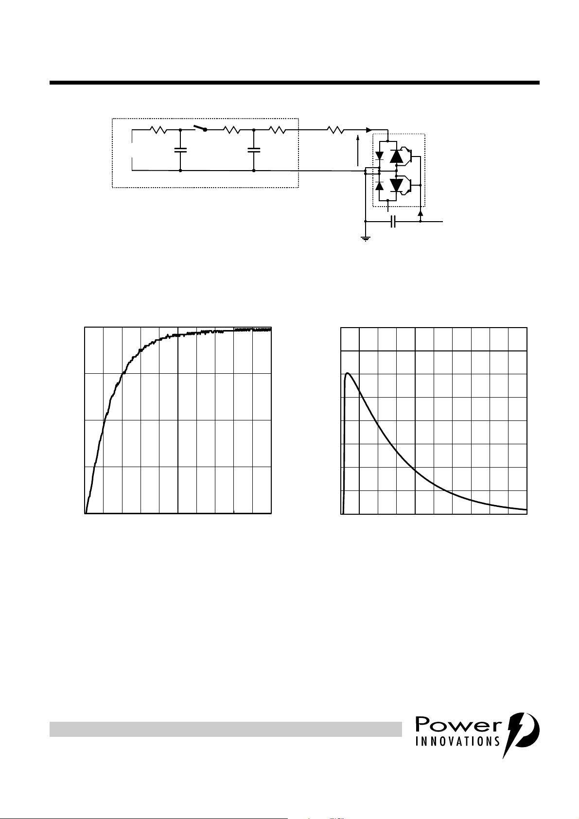
Figure 17 shows a typical TISPPB L2S SLIC card protection ci rcuit. The incoming line conduc tors, R and T,
connect to the relay matrix via the series over-current protection. Fusible resistors, fuses and positive
temperature coefficient (PTC) resistors can be used for over-current protection. Resistors will reduce the
prospective current from the surge generator for both the TISPPBL2S and the ring/test protector. The
TISP7xxxF3 protector has the sam e pr otection voltage for any ter mina l pair. This protector i s used when t he
ring generator configuration may be ground or battery-backed. For dedicated ground-backed ringing
generators, the TISP3xxxF3 gives better protection as its inter-conductor protection voltage is twice the
conductor to ground value.
Relay contacts 3a and 3b conn ect the line conductors to the SLIC via the TISPPBL2S protector. Closing
contacts 3a and 3b connects the TISP PBL2 S protector in parallel wi th the r ing/test protec tor. As the ring/test
protector requires much higher voltages than the TISPPBL2S to operate, it will only operate when the
contacts 3a and 3b are open. Both protectors will divert the same levels of peak surge current and their
PRODUCT INFORMATION
12
Page 13

TISPPBL2SD
PROGRAMMABLE OVERVOLTAGE PROTECTORS
FOR ERICSSON COMPONENTS PBL 3xxx SLICS
AUGUST 1999
TIP
WIRE
PBL 3xxx SLIC VOLTAGE WITHSTAND
AND TISPPBL2S VOLTAGE LIMITING
vs
TIME
PBL 386 20/1
PBL 386 20/1
V
V
V
V
V
V
V
Voltage - V
BATM
BATM
BATM
BATM
BATM
BATM
BATM
V
40
30
20
10
BATM
- 10
- 20
- 30
- 40
- 50
- 60
- 70
PBL 3762A
PBL 3796
TISPPBL2S
0
1 ms
10 µs
1 µs
0.25 µs
TISPPBL2S
PBL 3796
PBL 3762A
Figure 16. SLIC VOLTAGE WITHSTAND AND TISPPBL2S PROTECTION LEVELS
OVER-
CURRENT
PROTECTION
R1a
RING/TEST
PROTECTION
Th3
Th1
TEST
RELAY
S1a
RING
RELAY
S2a
SLIC
RELAY
S3a
PROTECTION
SLIC
AI6XBDS
R
P
Th4
Time10 ms
PBL
3xxx
SLIC
RING
WIRE
R1b
TISP
3xxxF3
OR
7xxxF3
Th2
S1b
TEST
EQUIP-
MENT
S2b
RING
GENERATOR
S3b
TISP
PBL2S
RP IS USED WHEN THE SLIC
HAS TERTIARY PROTECTION
Th5
R
C1
220 nF
P
V
AI6XAPS
Figure 17. TYPICAL APPLICATION CIRCUIT
required current ratings should be simila r. The TISPPBL2S protector gate reference voltage comes fr om the
SLIC negative supply (V
). A 220 nF gate capacitor sources the high gate current puls es caused by fast
BAT
rising impulses. When the SLIC has internal tertiary protection (e.g. PBL 386 21/1), then the two R
need to be added for protection co-ordination.
PRODUCT INFORMATION
BAT
resistors
P
13
Page 14

TISPPBL2SD
PROGRAMMABLE OVERVOLTAGE PROTECTORS
FOR ERICSSON COMPONENTS PBL 3xxx SLICS
AUGUST 1999
MECHANICAL DATA
D008
plastic small-outline package
This small-outline pa ckage consists of a circuit mo unted on a lead frame an d encapsulated with in a plastic
compound. The compound will withstand soldering temperature with no deformation, and circuit performance
characteristics will remain stable when operated in high humidity conditions. Leads require no additional
cleaning or processing when used in soldered assembly.
D008
6,20 (0.244)
5,80 (0.228)
1,75 (0.069)
1,35 (0.053)
4,00 (0.157)
3,81 (0.150)
8
1
7° NOM
3 Places
5,00 (0.197)
4,80 (0.189)
765
432
0,50 (0.020)
0,25 (0.010)
x 45°NOM
Designation per JEDEC Std 30:
PDSO-G8
5,21 (0.205)
4,60 (0.181)
0,203 (0.008)
0,102 (0.004)
0,79 (0.031)
0,28 (0.011)
ALL LINEAR DIMENSIONS ARE IN MILLIMETERS AND PARENTHETICALLY IN INCHES
NOTES: A. Leads are within 0,25 (0.010) radius of true position at maximum material condition.
B. Body dimensions do not include mold flash or protrusion.
C. Mold flash or protrusion shall not exceed 0,15 (0.006).
D. Lead tips to be planar within ±0,051 (0.002).
Pin Spacing
1,27 (0.050)
(see Note A)
6 Places
0,51 (0.020)
0,36 (0.014)
8 Places
0,229 (0.0090)
0,190 (0.0075)
PRODUCT INFORMATION
14
7° NOM
4 Places
1,12 (0.044)
0,51 (0.020)
4° ± 4°
MDXXAA
Page 15

TISPPBL2SD
PROGRAMMABLE OVERVOLTAGE PROTECTORS
FOR ERICSSON COMPONENTS PBL 3xxx SLICS
AUGUST 1999
IMPORTANT NOTICE
Power Innovations Limited (PI) reserves the right to make changes to its products or to discontinue any semiconductor product
or service without notice, and advises its customers to verify, before placing orders, that the information being relied on is
current.
PI warrants performance of its semiconductor products to the specifications applicable at the time of sale in accordance with
PI's standard wa rrant y. Testing and o t he r qu al ity c ontrol techniques are utilis ed to the extent PI deems necessary to support this
warranty. Specific testing of all parameters of each device is not necessarily performed, except those mandated by government
requirements.
PI assumes no liability for applications assistance, customer product design, software performance, or infringement of patents
or services described herein. Nor is any license, either express or implied, granted under any patent right, copyright, design
right, or other intellectual property right of PI covering or relating to any combination, machine, or process in which such
semiconductor products or services might be or are used.
PI SEMICONDUCTOR PRODUCTS ARE NOT DESIGNED, INTENDED, AUTHORISED, OR WARRANTED TO BE SUITABLE
FOR USE IN LIFE-SUPPORT APPLICATIONS, DEVICES OR SYSTEMS.
Copyright © 1999, Power Innovations Limited
PRODUCT INFORMATION
15
 Loading...