

Page 1
T
N
IA
L
P
S
M
N
E
O
L
IO
C
B
S
S
A
R
H
E
IL
o
V
A
V
*R
A
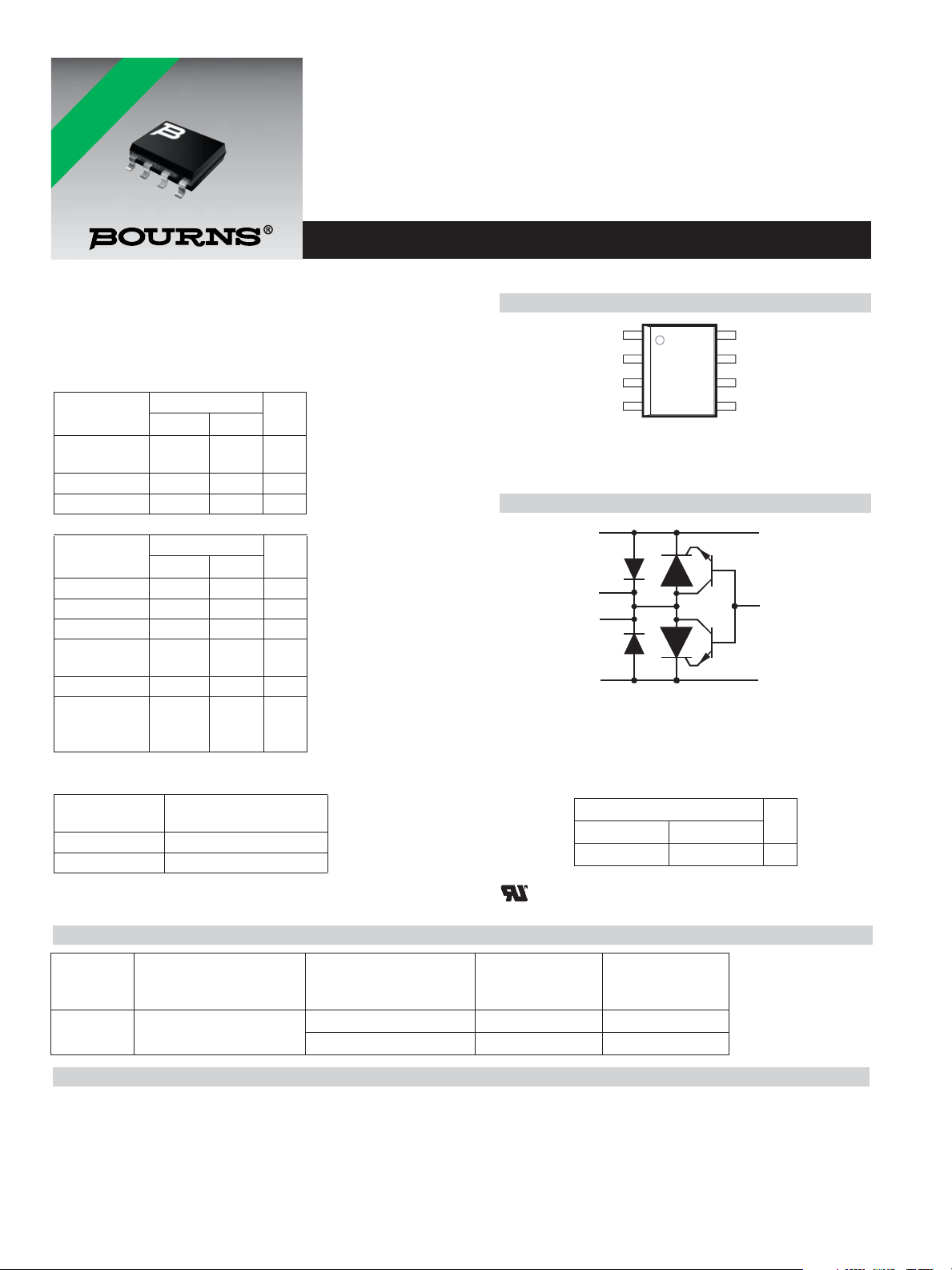
TISP61089B High Voltage Ringing SLIC Protector
DUAL FORWARD-CONDUCTING P-GATE THYRISTORS
PROGRAMMABLE OVERVOLTAGE PROTECTORS
TISP61089B
Dual Voltage-Programmable Protectors
- Supports Battery Voltages Down to -155 V
- Low 5 mA max. Gate Triggering Current
- High 150 mA min. Holding Current
Rated for LSSGR ‘1089 Conditions
Impulse
Waveshape
2/10
10/360 4.5.7 2, 5 30
10/1000 4.5.7 1,3 30
60 Hz Power
Fault Times
0.5 4.5.12 9 6.5
14.5.123, 4, 8 4.6
24.5.1273.4
5
30 4.5.12 6 1.3
900
‘1089 Test I
Sect ion T es t #
4.5.7
4.5.8
‘1089 Test I
Section Test #
4.5.12
4.5.1352, 3
4.5.12
4.5.13
4.5.15/16
1, 2
1, 4, 5 0.73
TSP
A
4
120
1
TSM
A
2.3
D Package (Top View)
(Tip)
(Gate)
(Ring)
K1
G
NC
K2
1
2
3
4
8
K1
7
A
6
A
5
K2
NC - No internal connection
Terminal typical applica tion name s shown in
parenthesis
Device Symbol
K1
A
A
K2
Te rminals K1, K2 and A correspond to the alternative
line designators of T, R and G or A, B and C. The
negative protection voltage is controlled by the
voltage, V
applied to the G terminal.
GG,
(Tip)
(Ground)
(Ground)
(Ring)
MD6XANB
K1
G
K2
SD6XAEB
2/10 Overshoot Voltage Specified
I
= 100 A, di/dt = 80A/µs
Element
Diode 10
SCR 12
TM
V
Rated for ITU-T K.20, K.21 and K.45
Waveshape
Voltage Curr ent
I
TSP
A
10/700 5/310 40
............................................ UL Recognized Components
How To Order
Device Package Carrier
TISP61089B D (8-pin Small-Outline)
Embossed Tape Reeled TISP61089BDR
For Standard
Te rmination Finish
Order As
Tube TISP61089BD
For Lead Free
Te rmination Finish
Order As
TISP61089BDR-S
TISP61089BD-S
Description
The TISP61089B is a dual forward-conducting buffered p-gate thyristor (SCR) overvoltage protector. It is designed to protect monolithic SLICs
(Subscriber Line Interface Circuits) against overvoltages on the telephone line caused by lightning, a.c. power contact and induction. The
TISP61089B limits voltages that exceed the SLIC supply rail voltage. The TISP61089B parameters are specified to allow equipment
compliance with Bellcore GR-1089-CORE, Issue 2 and ITU-T recommendations K.20, K.21 and K.45.
*RoHS Directive 2002/95/EC Jan 27 2003 including Annex
OCTOBER 2000 - REVISED FEBRUARY 2005
Customers should verify actual device performance in their specific applications.
Specifications are subject to change without notice.
Page 2

TISP61089B High Voltage Ringing SLIC Protector
Description (Continued)
The SLIC line driver section is typically powered from 0 V (ground) and a negative voltage in the region of -20 V to -150 V. The protector gate is
connected to this negative supply. This references the protection (clipping) voltage to the negative supply voltage. The protection voltage will
then track the negative supply voltage and the overvoltage stress on the SLIC is minimized.
Positive overvoltages are clipped to ground by diode forward conduction. Negative overvoltages are initially clipped close to the SLIC negative
supply rail value. If sufficient current is available from the overvoltage, then the protector SCR will switch into a low voltage on-state condition.
As the overvoltage subsides, the high holding current of TISP61089B SCR prevents d.c. latchup.
The TISP61089B is intended to be used with a series combination of a 40 Ω or higher resistance and a suitable overcurrent protector. Power
fault compliance requires the series overcurrent element to open-circuit or become high impedance (see Applications Information). For
equipment compliant to ITU-T recommendations K.20 or K.21 or K.45 only, the series resistor value is set by the coordination requirements.
For coordination with a 400 V limit GDT, a minimum series resistor value of 10 Ω is recommended.
These monolithic protection devices are fabricated in ion-implanted planar vertical power structures for high reliability and in normal system
operation they are virtually transparent. The TISP61089B buffered gate design reduces the loading on the SLIC supply during overvoltages
caused by power cross and induction. The TISP61089B is available in a 8-pin plastic small-outline surface mount package.
Absolute Maximum Ratings, -40 °C ≤ TJ ≤ 85 °C (Unless Otherwise Noted)
Rating Symbol Value Unit
Repetitive peak off-state voltage, V
Repetitive peak gate-cathode voltage, V
=0 V
GK
=0 V
KA
DRM
GKRM
-170 V
-167 V
Non-repetitive peak on-state pulse current (see Notes 1 and 2)
10/1000 µs(Telcordia (Bellcore) GR-1089-CORE, Issue 2, February 1999, Section 4)
5/320 µs (ITU-T K.20, K.21& K.45, K.44 open-circuit voltage wave shape 10/700 µs)
10/360 µs(Telcordia (Bellcore) GR-1089-CORE, Issue 2, February 1999, Section 4)
I
TSP
30
40
40
A
1.2/50 µs(Telcordia (Bellcore) GR-1089-CORE, Issue 2, February 1999, Section 4) 100
2/10 µs(Telcordia (Bellcore) GR-1089-CORE, Issue 2, February 1999,
Section 4) T
= 25 °C
J
120
170
Non-repetitive peak on-state current, 60 Hz (see Notes 1, 2 and 3)
0.5 s 6.5
1s
2s
I
5s
30 s
900 s
Non-repetitive peak gate current, 1/2 µspulse, cathodes commoned (see Notes 1 and 2) I
Operating free-air temperature range T
Junction temperature T
Storage temperature range T
TSM
GSM
A
J
stg
4.6
3.4
2.3
1.3
0.73
+40 A
-40 to +85 °C
-40 to +150 °C
-40 to +150 °C
A
NOTES: 1. Initially , the protector must be in thermal equilibrium with -40 °C
to its initial conditions.
2. The rated current values may be applied either to the Ring to Ground or to the Tip to Ground term inal pairs. Additionally, both
terminal pairs may have their rated current values applied simultaneously (in this case the Ground terminal current will be twice
the rated current value of an individual terminal pair). Above 85 °C, derate linearly to zero at 150 °C lead temperature.
3. Values f or V
OCTOBER 2000 - REVISED FEBRUARY 2005
Specifications are subject to change without notice.
Customers should verify actual device performance in their specific applications.
= -100 V. For values at other voltages see Figure 2.
GG
T
85 °C. The surge may be repeated after the device returns
≤
≤
J
Page 3

TISP61089B High Voltage Ringing SLIC Protector
Recommended Operating Conditions
Component Min Typ Max Unit
TISP61089B gate decoupling capacitor 100 220 nF
C
G
TISP61089B series resistor for GR-1089-CORE first-level surge survival 25
TISP61089B series resistor for GR-1089-CORE first-level and second-level surge survival 40 Ω
R
TISP61089B series resistor for GR-1089-CORE intra-building port surge survival 8
S
TISP61089B series resistor for K.20, K.21 and K.45 coordination with a 400 V primary
protector
Electrical Characteristics, TJ = 25 °C (Unless Otherwise Noted)
Parameter Test Condi ti o ns Min Typ Max Unit
V
(BO)
V
GK(BO)
V
V
FRM
I
I
GKS
I
GT
V
C
I
D
Off-state current VD=V
Breakover voltage2/10 µs, ITM=-100 A, di/dt = -80 A/µs, RS=50
Gate-cathode impulse
breakover voltage
F
Forward voltage IF=5A, tw= 200 µs3V
Peak forward recov ery
H
Holding current IT=-1A, di/dt = 1A/ms, VGG=-100 V -150 mA
Gate reverse current VGG=VGK=V
Gate trigger current IT=-3A, t
Gate-cathode trigger
GT
Cathode-anode off-
KA
state capacitance
voltage
voltage
2/10 µs, ITM=-100 A, di/dt = -80 A/µs, RS=50Ω, VGG= -100 V,
(see Note 4)
2/10 µs, I
I
T
f=1MHz, V
DRM
=-3A, t
, VGK=0
= 100 A, di/dt = 80 A/µs, RS=50Ω,(see Note 4) 10 V
F
, VKA=0
GKRM
≥ 20 µs, V
p(g)
≥ 20 µs, V
p(g)
=1V, IG=0, (see Note 5)
d
=-100 V 5 mA
GG
=-100 V 2.5 V
GG
10
T
= 25 °C-5µA
J
= 85 °C-50µA
T
J
VGG=-100 V -112 V
Ω,
12 V
T
= 25 °C-5µA
J
= 85 °C-50µA
T
J
V
=-3V 100 pF
D
V
=-48V 50 pF
D
Ω
Ω
Ω
NOTES: 4. The diode forward recovery and the thyristor gate impulse breakover (overshoot) are not strongly dependent of the gate supply
voltage value (V
GG
).
5. These capacitance measurements employ a three terminal capacitance bridge incor porating a guard circuit. The unmeasured
device terminals are a.c. connected to the guard terminal of the bridge.
Thermal Characteristics
Parameter Test Conditio n s Min Typ Max Unit
T
= 25 °C, EIA/JESD51-3 PCB, EIA/
R
θJA
Junction to free air thermal resistance
A
JESD51-2 environment, P
Customers should verify actual device performance in their specific applications.
TOT
= 1.7 W
OCTOBER 2000 - REVISED FEBRUARY 2005
Specifications are subject to change without notice.
120 °C/W
Page 4
TISP61089B High Voltage Ringing SLIC Protector
Parameter Measurement Information
-v
I
(BO)
Quadrant III
Switching
Characteristic
+i
I
(= ) |
FSP
TSP
Characteristic
I
(= ) |
FSM
TSM
I
F
V
F
V
GK(BO)
V
GG
I
S
V
(BO)
V
S
V
D
I
D
I
H
V
T
I
T
I
TSM
I
TSP
-i
Quadrant I
Forwar d
Conduction
+v
PM6XAAA
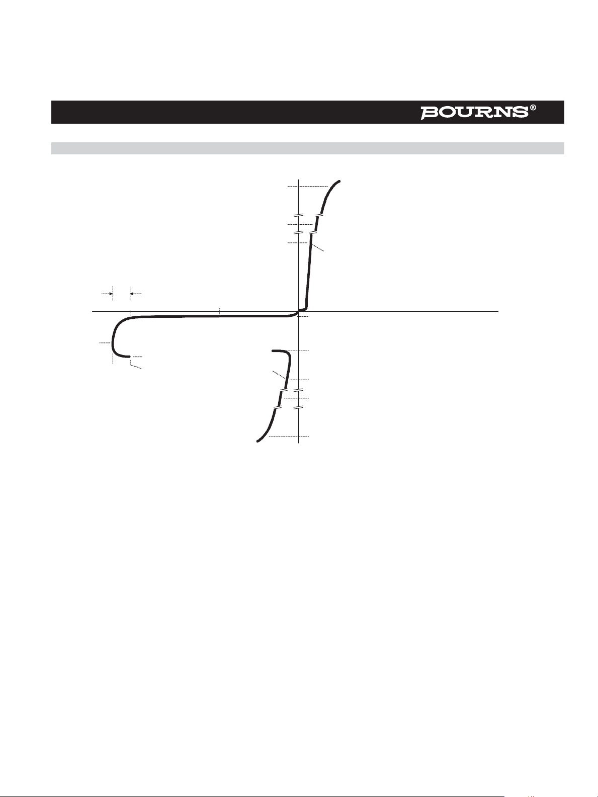
Figure 1. Voltage-Current Characteristic
Unless Otherwise Noted, All Voltages are Referenced to the Anode
OCTOBER 2000 - REVISED FEBRUARY 2005
Specifications are subject to change without notice.
Customers should verify actual device performance in their specific applications.
Page 5

TISP61089B High Voltage Ringing SLIC Protector
Thermal Information
PEAK NON-RECURRING AC
vs
20
15
10
8
7
6
5
4
3
2
1.5
1
0.8
— Peak Non-Recurrent 50 Hz Curr ent — A
0.7
TSM
I
0.6
0.5
0.01 0.1 1 10 100 1000
t — Current Duration — s
Figure 2. Non-Repetitive Peak On-State Current against
RING AND TIP TERMINALS:
Equal I
values applie d
TSM
simultaneously
GROUND TERMINAL:
Current twice I
TSM
EIA /JES D51
Environm ent and
PCB, T
VGG = -80 V
VGG = -100 V
VGG = -120 V
Duration
CURRENT DURATION
TI61AF
value
= 25 °C
A
VGG = -60 V
TYPICAL PEAK NON-RECURRING AC
vs
CURRENT DURATION
20
15
10
8
7
6
5
4
3
2
1.5
1
0.8
— Peak Non-Recurrent 50 Hz Current — A
0.7
TSM
I
0.6
0.5
0.01 0.1 1 10 100 1000
t — Current Duration — s
Figure 3. Typical No n-Repetitive Peak On-state Current
RING AND TIP TERMINALS:
Equal I
values appl ied
TSM
simultaneously
GROUND TERMINAL:
Current twice I
V
VGG = -100 V
VGG = -120 V
against Duration
value
TSM
Typical PCB
Mounting,
T
= 25 °C
A
= -80 V
GG
TI61DA
VGG = -60 V
OCTOBER 2000 - REVISED FEBRUARY 2005
Customers should verify actual device performance in their specific applications.
Specifications are subject to change without notice.
Page 6

TISP61089B High Voltage Ringing SLIC Protector
APPLICATIONS INFORMATION
Operation of Ringing SLICs using Multiple Negative Voltage Supply Rails
Figure 4 shows a typical powering arrangement for a multi-supply rail SLIC. V
switch S1 in the position shown, the line driver amplifiers are powered between 0 V and V
for short loop transmission. For long loops and to generate ringing, the driver voltage is increased by operating S1 to connect V
is a lower (smaller) voltage supply than V
BATL
. This mode minimizes the power consumption
BATL
BATH
conditions are shown in Figure 5.
SLIC
0 V
. With supply
. These
BATH
LINE
LINE
DRIVERS
Figure 4. SLIC with Voltage Supply Switching
0 V 0 V
V
BATL
S1
SUPPL Y
SWITCH
V
DCRING
V
PKRING
V
PKRING
V
BATL
V
BATH
AI6XCC
/2
/2
V
SLICG
V
PKRING
V
PKRING
0 V
/2
V
BATH
/2
V
SLICH
SHORT LOOP
LONG LOOP
V
BATH
RINGING
AI6XCD
V
BATH
Figure 5. Driver Supply Voltage Levels
Conventional ringing is typically unbalanced ground or battery backed. To minimize the supply voltage required, most multi-rail SLICs use
balanced ringing as shown in Figure 5. The ringing has d.c., V
has a peak value, V
internal losses in the SLIC from ground, V
10 V. This makes a total, V
, of 99 V. If the d.c. component was 20 V, then the total voltage swing needed would be 99 + 20 = 119 V. There are
PKRING
, supply rail value of 119 + 10 = 129 V.
BATH
, and the negative supply, V
SLICG
In some cases a trapezoidal a.c. ring signal is used. This would have a peak to r.m.s ratio (crest factor) of about 1.25, increasing the r.m.s. a.c.
ring level by 13 %. The d.c. ring voltage may be lowered for short loop applications.
OCTOBER 2000 - REVISED FEBRUARY 2005
Specifications are subject to change without notice.
Customers should verify actual device performance in their specific applications.
DCRING
, and a.c., V
SLICH
, components. A 70 V r.m.s. a.c. sinusoidal ring signal
PKRING
. The sum of these two losses generally amounts to a total of
Page 7

TISP61089B High Voltage Ringing SLIC Protector
SLIC Parameter Values
The table below shows some details of HV SLICs using multiple negative supply rails.
Manufacturer INFINEON‡ LEGERITY™‡
SLIC Series SLIC-P‡ ISLIC™‡
SLIC # PEB 4266 79R241 79R101 79R100
Data Sheet Issue 14/02/2001 -/08/2000 -/07/2000 -/07/2000
Short Circuit Current 110 150 150 150 mA
max. -155 -104 -104 -104 V
V
BA TH
max. -150 -104 V
V
BATL
AC Ri nging for: 85 45† 50† 55† V rms
Crest Factor 1.4 1.4 1.4 1.25
V
BATH
V
BA TR
R or T Power Max. < 10 ms 10 W
R or T Overshoot < 10 ms TBD T BD -5 5 -10 5 - 10 5 V
R or T Overshoot < 1 ms -10 +10 V
R or T Overshoot < 1 µs -10 +30 -10 10 -15 8 -15 8 V
R or T Overshoot < 250 ns -15 15 -20 12 -20 12 V
Line Feed Resistance 20 + 30 50 50 50
† Assumes -20 V battery voltage during ringing.
‡ Legerity, the Legerity logo and ISLIC are the trademarks of Legerity, Inc. (formerly AMD’s Communication Products Division).
Other product names used in this publication are for identification purposes only and may be trademarks of their respective
companies.
From the table, the maximum supply voltage, V
1 µs and -15 V, +12 V are needed for 250 ns. To maintain these voltage limits over the temperature range, 25 °C values of -12 V, +10 V are
needed for 250 ns.
-70 -90 -99 -99 V
-150 -36 -24 -24 V
, is -155 V. In terms of minimum voltage overshoot limits, -10 V and +8 V are needed for
BATH
BATH
V
BA TH
Unit
V
Ω
It is important to define the protector overshoot under the actual circuit current conditions. For example, if the series line feed resistor was
40 Ω, R1 in Figure 12, and Telcordia GR-1089-CORE 2/10 and 10/1000 first-level impulses were applied, the peak protector currents would be
56 A and 20 A. At the second-level, the 2/10 impulse current would be 100 A. Therefore, the protector voltage overshoot should be guaranteed
to not exceed the SLIC voltage ratings at 100 A, 2/10 and 20 A, 10/1000. In practice, as the 2/10 waveshape has the highest current (100 A)
and fastest di/dt (80 A/µs) the overshoot level testing can restricted to the be 2/10 waveshape.
Using the table values for maximum battery voltage and minimum overshoot gives a protection device requirement of -170 V and +12 V from
the output to ground. There needs to be temperature guard banding for the change in protector characteristics with temperature. To cover
down to -40 °C, the 25 °C protector minimum values become -185 V (V
) on the cathode and -182 V (V
DRM
) on the gate.
GKS
Gated Protectors
This section covers four topics. First, it is explained why gated protectors are needed. Second, the voltage limiting action of the protector is
described. Third, how the withstand voltages of the TISP61089B junctions are set. Fourth, an example application circuit is described.
Purpose of Gated Protectors
Fixed voltage thyristor overvoltage protectors have been used since the early 1980s to protect monolithic SLICs (Subscriber Line Interface
Circuits) against overvoltages on the telephone line caused by lightning, a.c. power contact and induction. As the SLIC was usually powered
from a fixed voltage negative supply rail, the limiting voltage of the protector could also be a fixed value. The TISP1072F3 is a typical example
of a fixed voltage SLIC protector.
OCTOBER 2000 - REVISED FEBRUARY 2005
Customers should verify actual device performance in their specific applications.
Specifications are subject to change without notice.
Page 8
TISP61089B High Voltage Ringing SLIC Protector
Gated Protectors (Continued)
SLICs have become more sophisticated. To minimize power consumption, some designs automatically adjust the driver supply voltage to a
value that is just sufficient to drive the required line current. For short lines, the supply voltage would be set low, but for long lines, a higher
supply voltage would be generated to drive sufficient line current. The optimum protection for this type of SLIC would be given by a protection
voltage which tracks the SLIC supply voltage. This can be achieved by connecting the protection thyristor gate to the SLIC V
BATH
supply,
Figure 6. This gated (programmable) protection arrangement minimizes the voltage stress on the SLIC, no matter what value of supply voltage.
WIRE
ΩΩΩΩ
600
GENERATOR
TIP
40
TISP61089B
R1
ΩΩΩΩ
SLIC
V
BATL
SOURCE
RESISTANCE
ΩΩΩΩ
600
40
R2
ΩΩΩΩ
SWITCHING MODE
POWER SUPPLY
I
SLIC
RING
WIRE
I
BATH
C2
D1
A.C.
GENERATOR
0 - 600 V r.m.s.
C1
220 nF
I
G
V
BATH
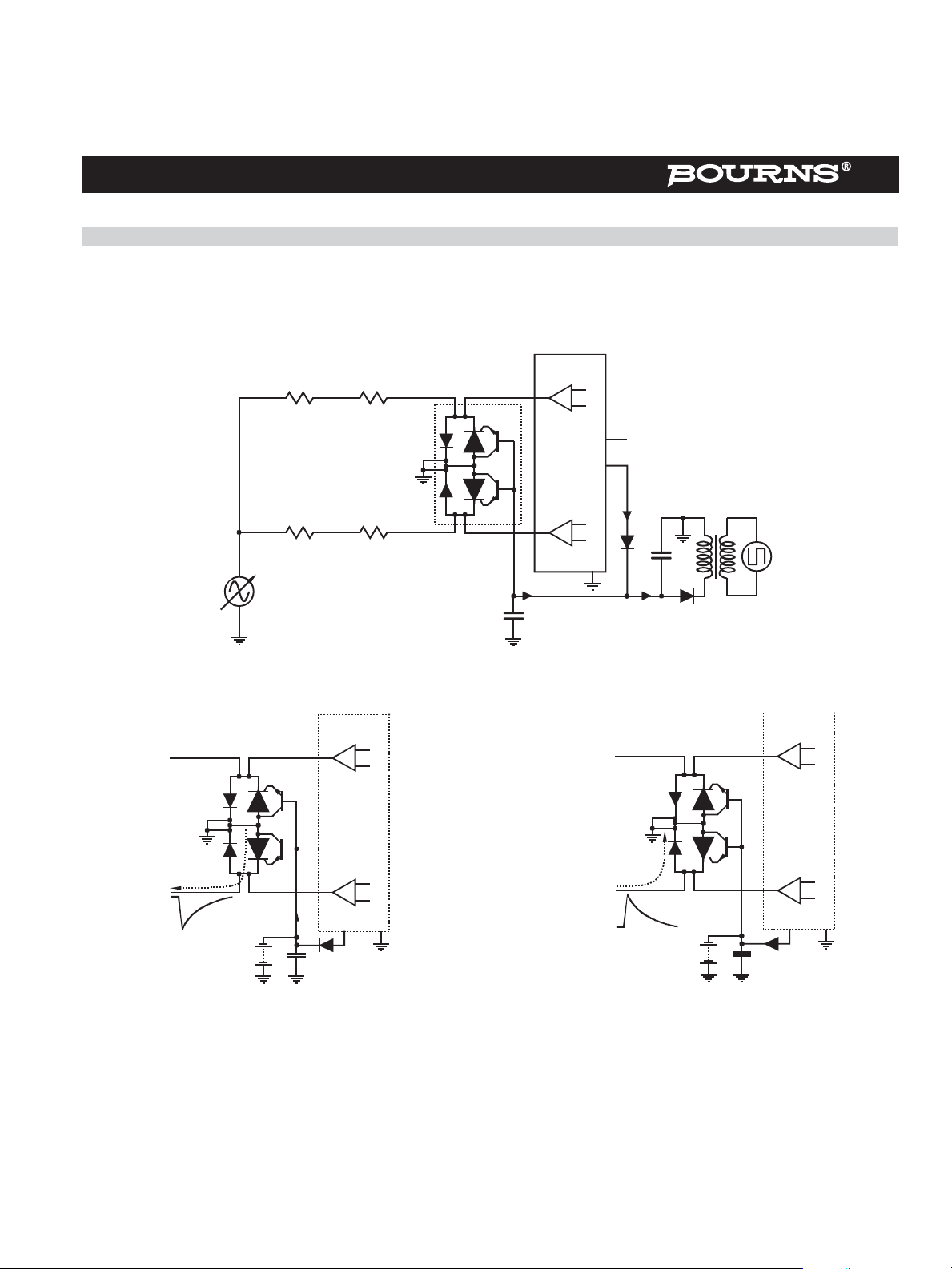
Figure 6. TISP61089B Buffered Gate Protector (‘1089 Section 4.5.12 Testing)
SLIC
PROTECTOR
SLIC
SLIC
PROTECTOR
Tx
AI6XCC
SLIC
TISP
61089B
BATH
Th5
I
G
220 nF
C1
I
K
AI6XAHB
V
Figure 7. Negative Overvoltage Condition
I
F
V
AI6XAIB
Figure 8. Positive Overvoltage Condition
TISP
61089B
BATH
Th5
C1
220 nF
Operation of Gated Protectors
Figure 7 and Figure 8 show how the TISP61089B limits negative and positive overvoltages. Positive overvoltages (Figure 8) are clipped by the
antiparallel diode of Th5 and the resulting current is diverted to ground. Negative overvoltages (Figure 7) are initially clipped close to the SLIC
negative supply rail value (V
condition. As the overvoltage subsides the high holding current of Th5 prevents d.c. latchup. The protection voltage will be the sum of the gate
supply (V
) and the peak gate-cathode voltage (V
BATH
). If sufficient current is available from the overvoltage, then Th5 will switch into a low voltage on-state
BATH
). The protection voltage will be increased if there is a long connection between the
GK(BO)
gate decoupling capacitor, C1, and the gate terminal. During the initial rise of a fast impulse, the gate current (IG) is the same as the cathode
current (IK). Rates of 80 A/µs can cause inductive voltages of 0.8 V in 2.5 cm of printed wiring track. To minimize this inductive voltage increase of
OCTOBER 2000 - REVISED FEBRUARY 2005
Specifications are subject to change without notice.
Customers should verify actual device performance in their specific applications.
Page 9
TISP61089B High Voltage Ringing SLIC Protector
Gated Protectors (Continued)
protection voltage, the length of the capacitor to gate terminal tracking should be minimized. Inductive voltages in the protector cathode wiring
will also increase the protection voltage. These voltages can be minimized by routing the SLIC connection through the protector as shown in
Figure 6.
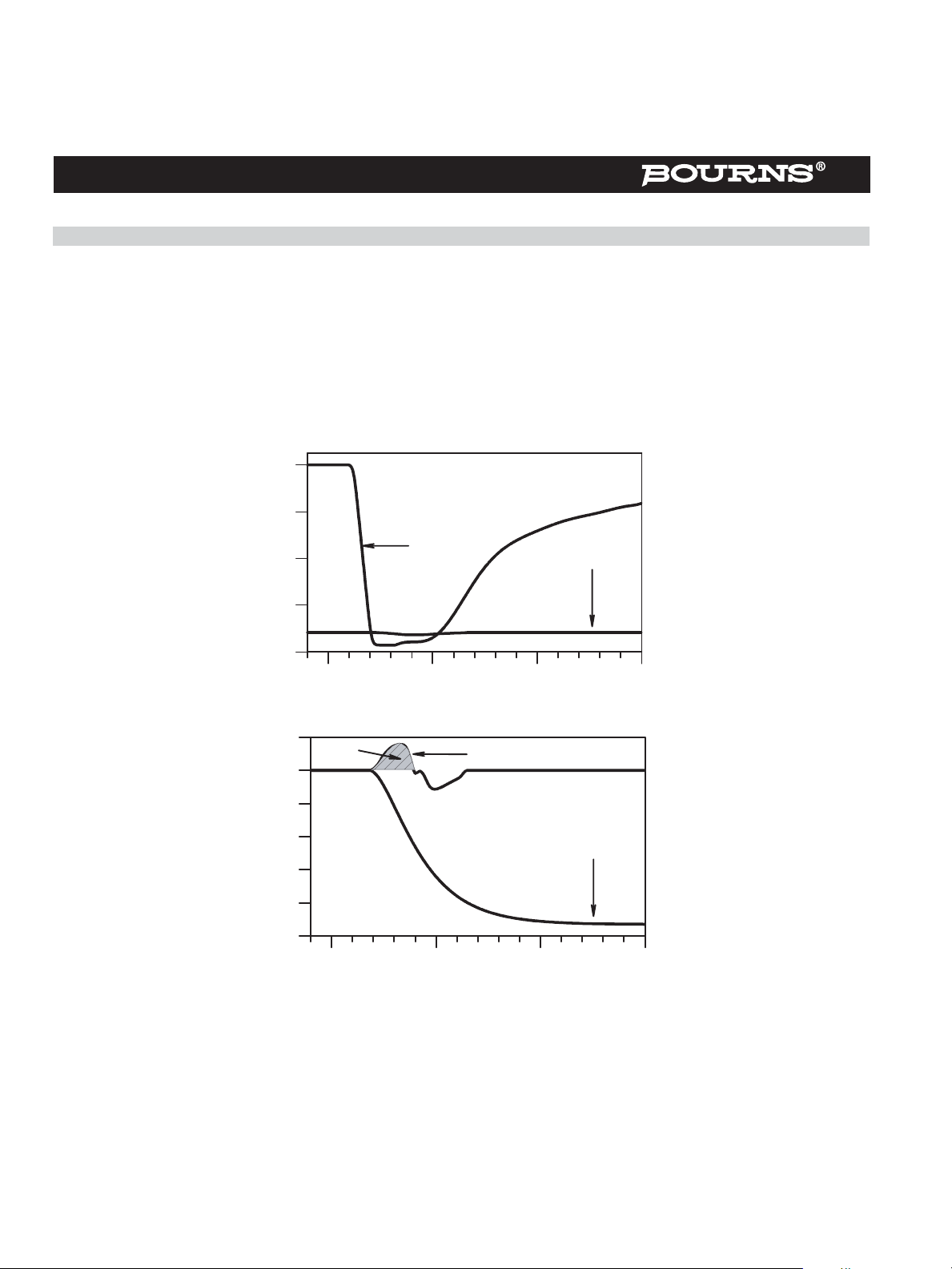
Figure 9, which has a 10 A/µs rate of impulse current rise, shows a positive gate charge (QGS) of about 0.1 µC. With the 0.1 µF gate
decoupling capacitor used, the increase in gate supply is about 1 V (= QGS/C1). This change is just visible on the -72 V gate voltage, V
But, the voltage increase does not directly add to the protection voltage as the supply voltage change reaches a maximum at 0.4 µs, when the
gate current reverses polarity, and the protection voltage peaks earlier at 0.3 µs. In Figure 9, the peak clamping voltage (V
increase of 5.5 V on the nominal gate supply voltage. This 5.5 V increase is the sum of the supply rail increase at that time, (0.5 V), and the
protection circuit’s cathode diode to supply rail breakover voltage (5 V). In practice, use of the recommended 220 nF gate decoupling capacitor
would give a supply rail increase of about 0.3 V and a V
0
-20
value of about -77.3 V.
(BO)
) is -77.5 V, an
(BO)
BATH
.
V
-40
Voltage - V
-60
-80
0.0 0.5 1.0 1.5
1
Q
GS
0
-1
-2
Current - A
-3
-4
-5
0.0 0.5 1.0 1.5
K
Time - µs
I
G
Time - µs
V
BATH
I
AI6XDE
K
Figure 9. Protector Fast Impulse C lamping and Switching Waveforms
Voltage Stress Levels on the TISP61089B
Figure 10 shows the protector electrodes. The package terminal designated gate, G, is the transistor base, B, electrode connection and so is
marked as B (G). The following junctions are subject to voltage stress: Transistor EB and CB, SCR AK (off state) and the antiparallel diode
(reverse blocking). This clause covers the necessary testing to ensure the junctions are good.
Testing transistor CB and EB: The maximum voltage stress level for the TISP61089B is V
diode voltage overshoot, V
the common (0 V) for this test (see Figure 10). The measured current, I
. The current flowing out of the G terminal is measured at V
FRM
, is the sum of the junction currents ICB and IEB.
GKS
Customers should verify actual device performance in their specific applications.
with the addition of the short term antiparallel
BATH
BATH
plus V
. The SCR K terminal is shorted to
FRM
OCTOBER 2000 - REVISED FEBRUARY 2005
Specifications are subject to change without notice.
Page 10

TISP61089B High Voltage Ringing SLIC Protector
Gated Protectors (Continued)
0 V
I
CB
B (G)
V
+ V
BATH
FRM
K
I
GKS
TISP
61 089B
I
EB
AI6XCE
Figure 10. Transistor CB and EB Verification
Testing transistor CB, SCR AK off state and diode reverse blocking: The highest AK voltage occurs during the overshoot period of the
protector. To make sure that the SCR and diode blocking junctions do not break down during this period, a d.c. test for off-state current, ID,
can be applied at the overshoot voltage value. To avoid transistor CB current amplification by the transistor gain, the transistor base-emitter is
shorted during this test (see Figure 11).
0 V
V
(BO)
TISP
I
R
61 089B
I
D
is the internal SCR value of
I
D(I)
I
CB
I
D(I)
A
B (G)
K
I
D
0 V
AI6XCF
Figure 11. Off-State Current Verification
Summary: Tw o tests are needed to verify the protector junctions. Maximum current values for I
voltage conditions.
OVER-
CURRENT
PROTECTION
RING/TEST
PROTECTION
TEST
RELAY
RING
RELAY
TIP
WIRE
R1a
Th1
S1a
S2a
Th3
and ID are required at the specified applied
GKS
SLIC
RELAY
S3a
SLIC
PROTECTOR
Th4
SLIC
RING
WIRE
R1b
TISP
3xxxF3
OR
Th2
S1b
7xxxF3
TEST
EQUIP-
MENT
Figure 12. Typical Application Circuit
OCTOBER 2000 - REVISED FEBRUARY 2005
Specifications are subject to change without notice.
Customers should verify actual device performance in their specific applications.
S2b
RING
GENERATOR
S3b
V
BATH
Th5
TISP
61089B
C1
220 nF
AI6XAJB
Page 11
TISP61089B High Voltage Ringing SLIC Protector
Application Circuit
Figure 12 shows a typical TISP61089B SLIC card protection circuit. The incoming line conductors, Ring (R) and Tip (T), connect to the relay
matrix via the series overcurrent protection. Fusible resistors, fuses and positive temperature coefficient (PTC) resistors can be used for
overcurrent protection. Resistors will reduce the prospective current from the surge generator for both the TISP61089B and the ring/test
protector. The TISP7xxxF3 protector has the same protection voltage for any terminal pair. This protector is used when the ring generator
configuration may be ground or battery-backed. For dedicated ground-backed ringing generators, the TISP3xxxF3 gives better protection as
its inter-conductor protection voltage is twice the conductor to ground value.
Relay contacts 3a and 3b connect the line conductors to the SLIC via the TISP61089B protector. The protector gate reference voltage comes
from the SLIC negative supply (V
). A 220 nF gate capacitor sources the high gate current pulses caused by fast rising impulses.
BATH
LSSGR 1089
GR-1089-CORE, “1089”, covers electromagnetic compatibility and electrical safety generic criteria for US network telecommunication
equipment. It is a module in Volume 3 of LSSGR (LATA (Local Access Transport Area) Switching Systems Generic Requirements,
FR-NWT-000064). In ‘1089, surge and power fault immunity tests are done at two levels. After first-level testing, the equipment shall not be
damaged and shall continue to operate correctly. Under second-level testing, the equipment shall not become a safety hazard. The equipment
is permitted to fail as a result of second-level testing. When the equipment is to be located on customer premises, second-level testing
includes a wiring simulator test, which requires the equipment to reduce the power fault current below certain values.
The following clauses reference the ‘1089 section and calculate the protector stress levels. The TISP61089B needs a 40 Ω series resistor to
survive second-level surge testing. To survive first-level testing and possibly fail under second-level testing allows lower resistor value of 25 Ω
to be used. Tabulated current values are given for both 40 Ω and 25 Ω series resistor values.
‘1089 Section 4.5.5 - Test Generators
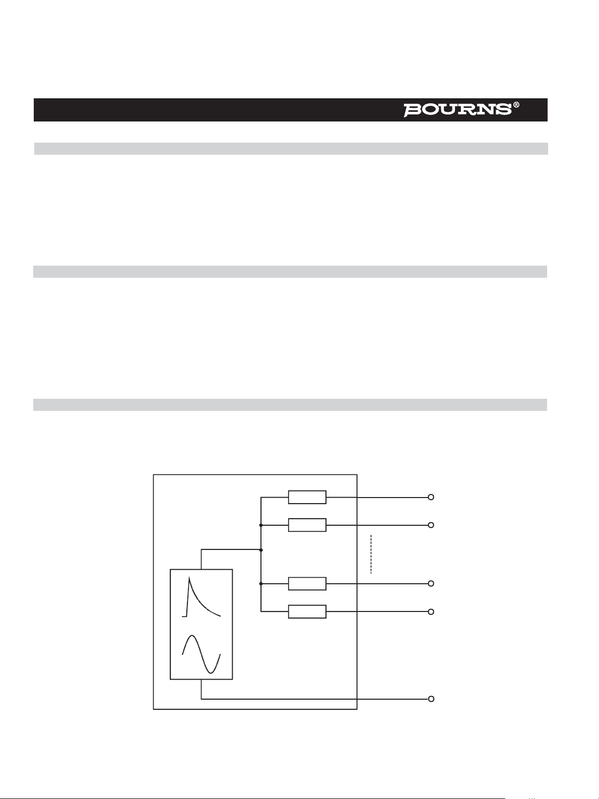
The generic form of test generator is shown in Figure 13. It emphasises that multiple outputs must be independent, i.e. the loading condition of
one output must not affect the waveforms of the other outputs. It is a requirement that the open-circuit voltage and short circuit current
waveforms be recorded for each generator output used for testing. The fictive impedance of a generator output is defined as the peak opencircuit voltage divided by the peak short-circuit current. Specified impulse waveshapes are maximum rise and minimum decay times. Thus, the
10/1000 waveshape should be interpreted as <10/>1000 and not the usually defined nominal values which have a tolerance.
Z
Z
Z
Z
or
Z is the fictiv e
curr ent-limiting
impedance in
each output feed
Outp ut 1
Output 2
Output n
Output n + 1
Return
Generic Lightning or AC Test Gener a tor
Figure 13. ‘1089 Test Generators
AI6XCJ
OCTOBER 2000 - REVISED FEBRUARY 2005
Customers should verify actual device performance in their specific applications.
Specifications are subject to change without notice.
Page 12
TISP61089B High Voltage Ringing SLIC Protector
‘1089 Section 4.5.5 - Test Generators (Continued)
The exception to these two conditions of independence and limit waveshape values is the alternative IEEE C.62.41, 1.2/50-8/20 combination
wave generator which may be used for testing in ‘1089 Sections 4.5.7, 4.5.8 and 4.5.9. Here, the quoted waveshape values are nominal with
defined tolerance. The open-circuit voltage waveshape is 1.2 µs±0.36 µs front time and 50 µs±10 µs duration. The short-circuit current
waveshape is 8 µs+1.0 µs, -2.5 µs front time and 20 µs+8 µs, -4 µs duration. The generator fictive source impedance (peak open-circuit
voltage divided by peak short-circuit current) is 2.0 Ω±0.25 Ω.
To get the same peak short-circuit currents as the 2/10 generator, for the same peak open-circuit voltage setting, ‘1089 specifies that the
1.2/50-8/20 generator be used with external resistors for current limiting and sharing. When working into a finite resistive load, the delivered
1.2/50-8/20 generator current waveshape moves towards the 1.2/50 voltage waveshape. Thus, although the 1.2/50-8/20 delivered peak
current is similar to the 2/10 generator, the much longer current duration means that a much higher stress is imposed on the equipment
protection circuit. This can cause fuses to operate which are perfectly satisfactory on the normal 2/10 generator. Testing with the 1.2/50-8/20
generator gives higher stress levels than the 2/10 generator and, because it is seldom used, will not be covered in this analysis.
Output 1Ring
V1
Return
Test G enerator
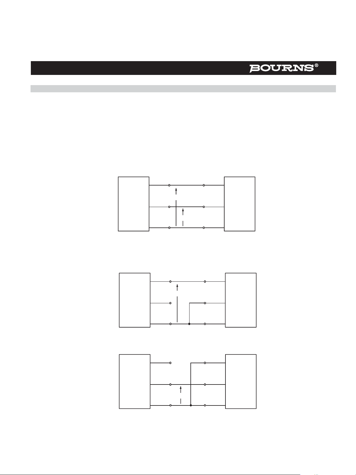
Figure 14. Longitudinal (also Called Common Mode) Testing
Output 1Ring
Return
Tes t Generator
Outp ut 1 Rin g
V2
V1
TipOutput 2
Ground
TipOutput 2
Ground
AI6XCK
EUT
(Equipment
Under Test)
EUT
(Equipment
Under Test)
Return
Tes t Generato r
Figure 15. Transverse (also Called Differential or Metallic) Testing
OCTOBER 2000 - REVISED FEBRUARY 2005
Specifications are subject to change without notice.
Customers should verify actual device performance in their specific applications.
V2
TipOutput 2
Ground
AI6XCM
EUT
(Equipment
Under Test)
Page 13

TISP61089B High Voltage Ringing SLIC Protector
‘1089 Section 4.5.6 - Test Connections
The telecommunications port R and T terminals may be tested simultaneously or individually. Figure 14 shows connection for simultaneous
(longitudinal) testing. Figure 15 shows the two connections necessary to individually test the R and T terminals during transverse testing.
The values of protector current are calculated by dividing the open-circuit generator voltage by the total circuit resistance. The total circuit
resistance is the sum of the generator fictive source resistance and the TISP61089B series resistor value. The starting point of this analysis is
to calculate the minimum circuit resistance for a test by dividing the generator open-circuit voltage by the TISP61089B rating. Subtracting the
generator fictive resistance from the minimum circuit resistance gives the lowest value of series resistance that can be used. This is repeated
for all test connections. As the series resistance must be a fixed value, the value used has to be the highest value calculated from all the
considered test connections. Where both 10/1000 and 2/10 waveshape testing occurs, the 10/1000 test connection gives the highest value of
minimum series resistance. Unless otherwise stated, the analysis assumes a -40 °C to +85 °C temperature range.
‘1089 Section 4.5.7 - First-Level Lightning Surge Testing
Table 1 shows the tests for this section. The peak TISP61089B current, ITM, is calculated by dividing the generator open voltage by the sum of
the generator fictive source and the line feed, RS, resistance values. Columns 9 and 10 show the resultant currents for RS values of 25 Ω and
40 Ω. The TISP61089B rated current values at the various waveshapes are higher than those listed in Table 1. Used with the specified values
of RS, the TISP61089B will survive these tests.
Table 1. First-Level Surge Currents
Surge
NOTES: 1. Surge 3 may be used instead of Surge 1 and Surge 2.
Waveshape
#
1 10/1000 600 100 +25, -25 Transv erse &
2 10/360 1000 100 +25, -25 Transverse &
3 10/1000 1000 100 +25, -25 Transv erse &
42/10 2500 500 +10, -10 Longitudinal No 5 2x83 2x56
5 10/360 1000 25 +5, -5 Longitudinal No 40 2x15 2x13
2. Surge 5 is applied to multiple line pairs up to a maximum of 12.
3. If the equipment contains a voltage-limiting secondary protector, each test is repeated at a voltage just below the threshold of
limiting.
Open-circuit
Vol tage
V
Short-circuit
Current
A
No
of
Tests
Test
Connections
Longitudinal
Longitudinal
Longitudinal
Primary
Fitted
No 6 19 &
No 10 29 &
No 10 29 &
Generator
Fictive
Source
Resistance
Ω
TISP61089B I
R
= 25
Ω
s
2x19
2x29
2x29
A
TM
Rs = 40
13 &
2x13
20 &
2x20
20 &
2x20
Ω
‘1089 Section 4.5.8 - Second-Level Lightning Surge Testing
Table 2 shows the 2/10 test used for this section. Columns 9 and 10 show the resultant currents for RS values of 25 Ω and 40 Ω. Used with an
RS of 40 Ω, the TISP61089B with survive this test. The 25 Ω value of RS is only intended to give first-level (Section 4.5.7) survival. Under
second-level conditions, the peak current will be 2x143 A, which may result in failure of the 2x120 A rated TISP61089B. However, if the testing
is done at or near 25 °C, the TISP61089B will survive with an RS value of 25 Ω as the 2/10 rating is 170 A at this temperature.
Table 2. Second-Level Surge Current
Generato
Surge
NOTE: 1. If the equipment contains a voltage-limiting secondary protector, the test is repeated at a voltage just below the threshold of
Waveshape
#
12/10 5000 500 +1, -1 Longitudinal No 10 2x143 2x100
limiting.
Open-circuit
Vol tage
V
Short-circuit
Current
A
No
of
Tests
Te st
Connections
Customers should verify actual device performance in their specific applications.
Primary
Fitted
Resistance
Specifications are subject to change without notice.
r
Fictive
Source
ΩΩΩΩ
OCTOBER 2000 - REVISED FEBRUARY 2005
TISP61089B I
= 25
R
ΩΩΩΩ
s
A
Rs = 40
TM
ΩΩΩΩ
Page 14
TISP61089B High Voltage Ringing SLIC Protector
‘1089 Section 4.5.9 - Intra-Building Lightning Surge Testing
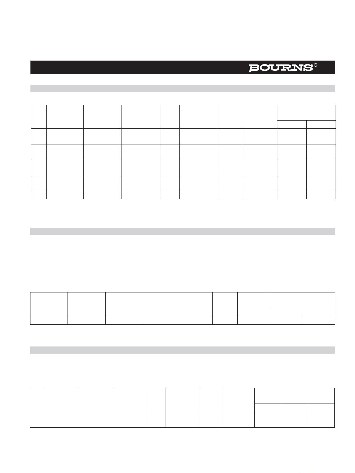
This test is for network equipment ports that do not serve outside lines. Table 3 shows the 2/10 tests used for this section. Dedicated intrabuilding ports may use an RS value of 8 Ω. The 8 Ω value is set by the intra-building second-level a.c. testing of Section 4.5.16. Columns 9, 10
and 11 show the resultant currents for RS values of 8 Ω, 25 Ω and 40 Ω. The listed currents are lower than the TISP61089B current rating of
2x120 A and the TISP61089B will survive these tests.
Table 3. Intra-building Lightning Surge Currents
Generator
Surge
NOTE:1.If the equipment contains a voltage-limiting secondary protector, the test is repeat ed at a voltage just below the threshold of
Waveshape
#
12/10 800 100 +1, -1 Transverse NA 8 50 24 17
22/10 1500 100 +1, -1 Longitudinal NA 15 2x65 2x38 2x27
limiting.
Open-circuit
Voltage
V
Short-circuit
Current
A
No
of
Tests
Test
Connections
Primary
Fitted
Fictive
Source
Resistance
ΩΩΩΩ
R
= 8
s
ΩΩΩΩ
TISP61089B I
A
Rs = 25
ΩΩΩΩ
TM
Rs = 40
ΩΩΩΩ
‘1089 Section 4.5.11 - Current-Limiting Protector Testing
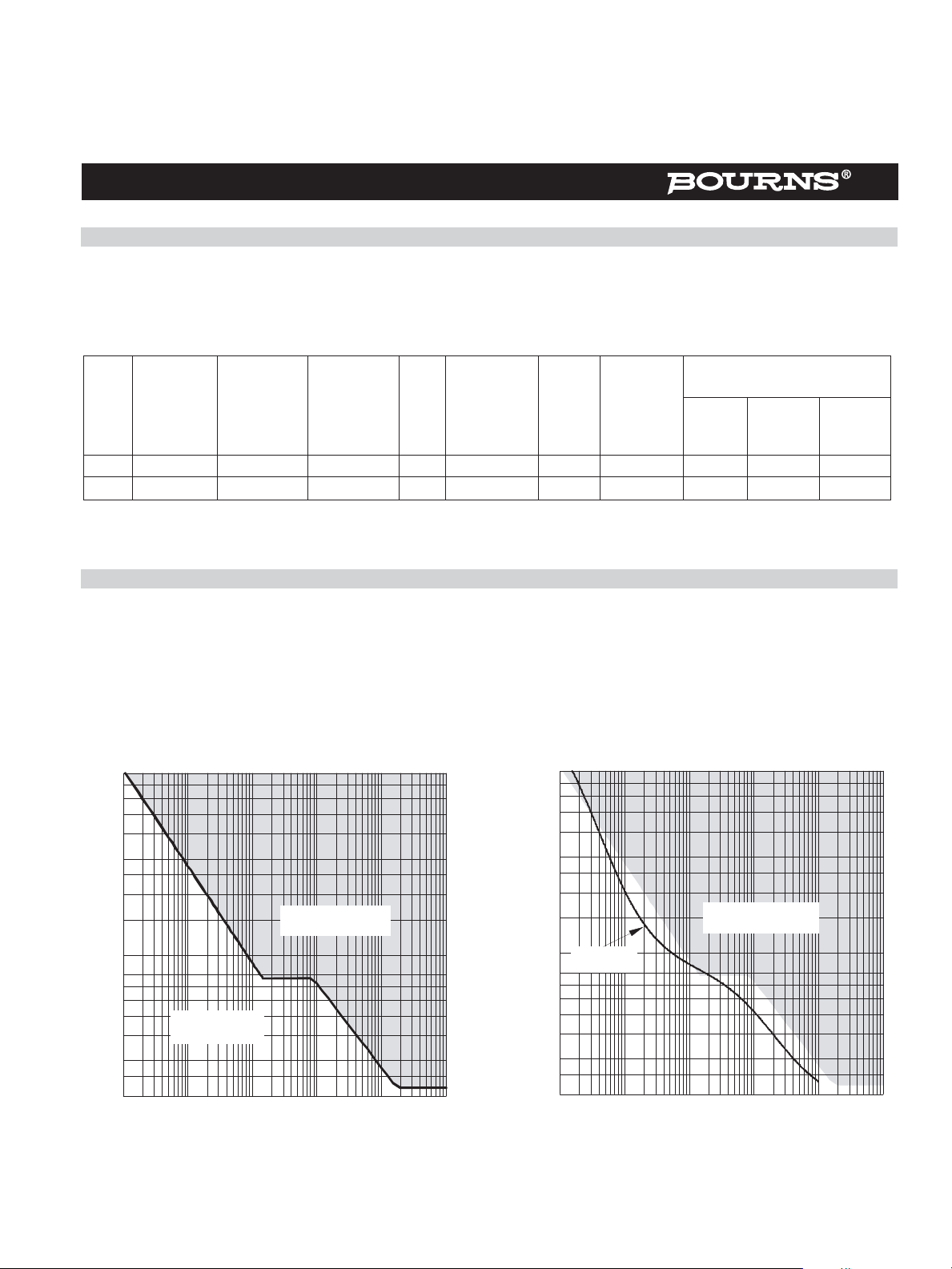
Equipment that allows unacceptable current to flow during power faults (Figure 16) shall be specified to use an appropriate current-limiting
protector. The equipment performance can be determined by testing with a series fuse, which simulates the safe current levels of a telephone
cable. If this fuse opens, the equipment allows unacceptable current flow and an external current-limiting protector must be specified. For
acceptable currents, the equipment must not allow current flows for times that would operate the simulator. The wiring simulator fuse currenttime characteristic shall match the boundary of Figure 16. A Bussmann MDQ-1 6/10 fuse is often specified as meeting this requirement, Figure 17.
'1089 WIRI NG SI MULATOR CURRENT
vs
TIME
80
70
60
50
40
30
25
20
15
10
8
Current — A rms
7
6
5
4
3
2.5
2
0·01 0·1
ACCEPTABLE
REGION
t - Current Durat ion - s
Figure 16. Wiring Simulator Current-Time
UNACCEPTABLE
REGION
1101001000
TI6LAG
Curr ent — A rm s
80
70
60
50
40
30
25
20
15
10
2.5
MDQ-16/10 OPERATING CURRENT
vs
AVERAGE MEL T TIME
UNACCEPTABLE
REGION
MDQ-16/
8
7
6
5
4
3
2
0·01 0·1 1 10 100 1000
10
t - Current Durati on - s
Figure 17. MDQ-16/10 Current-Time
TI6LAH
OCTOBER 2000 - REVISED FEBRUARY 2005
Specifications are subject to change without notice.
Customers should verify actual device performance in their specific applications.
Page 15

TISP61089B High Voltage Ringing SLIC Protector
‘1089 Section 4.5.11 - Current-Limiting Protector Testing (Continued)
The test generator has a voltage source that can be varied from zero to 600 V rms and an output resistance of 20 Ω to each conductor. Table 4
shows the range of currents conducted by the TISP61089B.
Table 4. Wiring Simulator Testing
AC Duration
s
900 0 to 600 0 to 30 Transverse & Longitudinal No 20 0 to 2x 19 0 to 2x 14
Open-Circuit
RMS Voltage
V
Short-Circuit
RMS Current
A
Tes t
Connections
Primary
Fitted
Source
Resistance
ΩΩΩΩ
TISP61089B I
A (peak)
R
= 25ΩRs = 40
s
TM
‘1089 Section 4.5.12 - First-Level Power Fault Testing
Table 5 shows the nine tests used for this section. The TISP61089B will survive these peak current values as they are lower than the
TISP61089B current-time ratings.
Table 5. First-Level Power Fault Currents
Test#AC Duration
s
1 900 50 0.33 1
2 900 100 0.17 1
31
41 1000 1 60 Longitudinal Yes 1000 2x1.38 2x1.30
55 600 0.09 60 Differential No Capacitive 2x0.12 2x0.12
630 600 0.5 1
72 600 2.2 1
81 600 3.0 1
90.5 1000 5 1 Longitudinal Yes 200 2x6.28 2x5.89
NOTES: 1. If the equipment contains a voltage-limiti ng device or a current -limiting device, tests 1, 2 and 3 are repeated at a level just below
the thresholds of the limiting devices.
2. Test 5 uses a special circuit with transformer coupled a.c. and capacitive feed.
3. Tests 1 through 5 are requirements and the equipment shall not be damaged after these tests.
4. Tests 6 through 9 are desirable objectives and the equipment can be damaged after these tests.
Open-circuit
RMS Voltage
V
200
400
600
Short-circuit
RMS Current
A
0.33
0.67
1.00
No
of
Tests
60
60
60
Te st
Connections
Tr a n sv e rs e &
Longitudinal
Tr a n sv e rs e &
Longitudinal
Tr a n sv e rs e &
Longitudinal
Tr a n sv e rs e &
Longitudinal
Tr a n sv e rs e &
Longitudinal
Tr a n sv e rs e &
Longitudinal
Primary
Fitted
No 150 2x0.40 2x0.37
No 600 2x0.23 2x0.22
No 600
No 1200 2x0.69 2x0.68
No 273 2x2.85 2x2.71
No 200 2x3.77 2x3.54
Source
Resistance
ΩΩΩΩ
TISP61089B I
A (peak)
= 25
R
Ω
s
2x0.45
2x0.90
2x1.36
TM
Rs = 40
2x0.44
2x0.89
2x1.33
ΩΩΩΩ
ΩΩΩΩ
‘1089 Section 4.5.13 - Second-Level Power Fault Testing for Central Office Equipment
Table 6 shows the five tests used for this section. Columns 9 and 10 show the prospective currents for these tests using RS values of 25 Ω and
40 Ω. The two most stressful tests of this section are test 1 and test 2. As shown in Table 6, the peak currents for these tests are 2x17 A and
2x7.7 A respectively. With the exception of test 5, all the other tests require the series overcurrent protection to operate before the TISP61089B
current-time ratings are exceeded. In the case of test 2, with an RS of 25 Ω, the overcurrent protection must operate within the initial a.c. half
cycle to prevent damage.
OCTOBER 2000 - REVISED FEBRUARY 2005
Customers should verify actual device performance in their specific applications.
Specifications are subject to change without notice.
Page 16
TISP61089B High Voltage Ringing SLIC Protector
‘1089 Section 4.5.13 - Second-Level Power Fault Testing for Central Office Equipment (Continued)
Table 6. Second-Level Power Fault Currents
Test#AC Duration
s
1 900
25 600 60 1
35 600 7 1
4 900
5 900 600 0.09 60 Differential No Capacitive 2x0.09 2x0.09
NOTES: 1. If the equipment contains a voltage-limiting device or a current-limiting device, these tests are repeated at a level just below the
thresholds of the limiting devices.
2. Test 5 uses a special circuit with transformer coupled a.c. and capacitive feed.
Open-circuit
RMS Voltage
V
120
277
100 to
600
Short-cir cuit
RMS Current
A
25
0.37 to
2.2
No
of
Tests
1
1
Test
Connect ions
Transverse &
Longitudinal
Transverse &
Longitudinal
Transverse &
Longitudinal
Transverse &
Longitudinal
Primary
Fitted
No
No 10 2x24 2x17
No 86 2x7.7 2x6.8
No 270 2x2.9 2x2.7
Source
Resistance
ΩΩΩΩ
5
11
TISP61089B I
A (peak)
= 25
R
Ω
s
2x5.7
2x11
TM
Rs = 40
2x3.8
2x7.7
ΩΩΩΩ
‘1089 Section 4.5.15 - Second-Level Power Fault Testing for Equipment Located on the Customer Premise
This test, Table 7, is for network equipment located on the customer premises. The purpose is to ensure that the feed wiring does not become
a hazard due to excessive current. This testing is similar to the Section 4.5.11 testing. If the equipment is directly wired, the wiring simulator
described in Section 4.5.11 is replaced by a one-foot section of 26 AWG wrapped in cheesecloth. The equipment fails if an open circuit occurs
or the cheesecloth is damaged.
Table 7 shows the test conditions for this section. Columns 7 and 8 show the prospective currents using RS values of 25 Ω and 40 Ω. For the
TISP61089B to survive, the series overcurrent protection to operate before the TISP61089B current-time ratings are exceeded.
Table 7. Customer Premise Wiring Simulator Testing
AC Duration
s
900 0 to 600 0 to 30 Transverse & Longitudinal No 20 0 to 2x 19 0 to 2x 14
NOTE:1.If the equipment interrupts the current before the 600 V r ms level is reached, a second piece of equipment is tested. The second
Open-circuit
RMS Voltage
V
piece of equipment shall withstand 600 V rms applied for 900 s without causing a hazard.
Short-circuit
RMS Curr ent
A
Test
Connections
Primary
Fitted
Source
Resistance
ΩΩΩΩ
TISP61089B I
A (peak)
= 25
Ω
R
s
TM
Rs = 40
ΩΩΩΩ
‘1089 Section 4.5.16 - Second-Level Intra-Building Power Fault Testing for Equipment Located on the Customer Premise
This test, Table 8, is for network equipment ports that do not serve outside lines. For standard plugable premise wiring, the wiring simulator
fuse shall be used for testing. Where direct wiring occurs, the simulator shall consist of a length of the wire used wrapped in cheesecloth. The
equipment fails if a hazard occurs or a wiring simulator open circuit occurs or the cheesecloth is damaged.
Table 8. Second-Level Power Fault Currents
R
= 8
s
TISP61089B I
A (peak)
Rs = 25ΩRs = 40
Ω
TM
Tes t#AC Duration
s
1900 120 25 1
NOTE:1.If the equipment contain s a voltage-limiting device or a current-limiting device, these tests are repeated at a level just below the
OCTOBER 2000 - REVISED FEBRUARY 2005
Specifications are subject to change without notice.
Customers should verify actual device performance in their specific applications.
thresholds of the limiting devices.
Open-circuit
RMS Voltage
V
Short-circuit
RMS Current
A
No
of
Tests
Tes t
Connections
Transverse &
Longitudinal
Prima ry
Fitted
No 5 2x13 2x5.7 2x3.8
Source
Resistance
ΩΩΩΩ
ΩΩΩΩ
Page 17
TISP61089B High Voltage Ringing SLIC Protector
‘1089 Section 4.5.16 (Continued)
Dedicated intra-building ports may use an RS value of 8 Ω. The 8 Ω value limits the initial current to 13 A, which is within the TISP61089B
single cycle rating. For the TISP61089B to survive the full 900 s test, the series overcurrent protection to operate before the TISP61089B
current-time ratings are exceeded.
Overcurrent and Overvoltage Protection Coordination
To meet ‘1089, the overcurrent protection must be coordinated with the requirements of Sections 4.5.7, 4.5.8, 4.5.9, 4.5.12, 4.5.13, 4.5.15 and
the TISP61089B. The overcurrent protection must not fail in the first-level tests of Sections 4.5.7, 4.5.9 and 4.5.12 (tests 1 through 5). Test 6
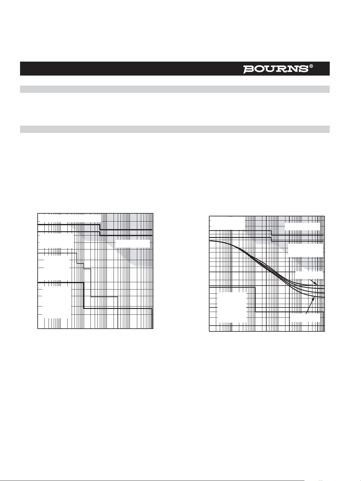
through 9 of Section 4.5.12 are not requirements. The test current levels and their duration are shown in Figure 18. First-level tests have a high
source resistance and the current levels are not strongly dependent on the TISP61089B series resistor value.
Second-level tests have a low source resistance and the current levels are dependent on the TISP61089B RS resistor value. The two stepped
lines at the top of Figure 18 are for the 25 Ω and 40 Ω series resistor cases. The unacceptable current region (Section 4.5.11) is also shown in
Figure 18. If current flows for the full second-level test time, the unacceptable current region will be entered. The series overcurrent protector
must operate before the unacceptable region is reached.
MAXIMUM RMS CURRENT
vs
30
TIME
Second Level Tests, 25
20
10
Second Level
7
Tests, 40 Ω
5
Objective
3
First Level
2
Tests # 6
through 9
1
0.7
First Level
0.5
Maximum RMS Current - A
Tests # 1
through 5,
0.3
0.2
25 ΩΩΩΩ & 40 Ω
0.1
0.01 0.1 1 10 100 1000
Ω
ΩΩ
Ω
ΩΩ
Figure 18. ‘1089 Test Current Levels
Fusible overcurrent protectors cannot operate at first-level current levels. Thus, the permissible low current time-current boundary for fusible
overcurrent protectors is formed by the first-level test currents. Automatically resettable overcurrent protectors (e.g. Positive Temperature
Coefficient Thermistors) may operate during first-level testing, but normal equipment working must be restored after the test has ended.
Ω
Unacceptable
Time - s
AI6XAKB
50
Second Level
40
Tests, 25 Ω
30
20
15
10
8
6
5
4
3
2
1.5
1
Fir st Level
Tests # 1
through 5,
25 ΩΩΩΩ & 40 Ω
0.01 0.1 1 10 100 1000
Peak 50 Hz / 60 Hz Current — A
0.8
0.6
0.5
0.4
0.3
0.2
0.15
Figure 19. TISP61089B Overlay
PEAK AC
vs
CURRENT DURATION
Ω
ΩΩ
Ω
ΩΩ
t — Current Duration — s
Unacceptable
AI6XDM
Second Level
Tests, 40 Ω
V
VGG = -60 V
= -120 V
GG
Ω
ΩΩ
At system level, the high current boundary is formed by the unacceptable region. However, component and printed wiring, PW, current
limitations will typically lower the high current boundary. Although the series line feed resistance, RS, limits the maximum available current in
second-level testing, after about 0.5 s this limitation will exceed the acceptable current flow values.
These three boundaries, first-level, second-level and unacceptable, are replotted in terms of peak current rather than rms current values in
Figure 19. Using a peak current scale allows the TISP61089B longitudinal current rating curves (Figure 3) to be added to Figure 19. Assuming
the PW is sized to adequately carry any currents that may flow, the high current boundary for the overcurrent protector is formed by the
TISP61089B rated current. Note that the TISP61089B rated current curve also depends on the value of gate supply voltage.
OCTOBER 2000 - REVISED FEBRUARY 2005
Customers should verify actual device performance in their specific applications.
Specifications are subject to change without notice.
Page 18
TISP61089B High Voltage Ringing SLIC Protector
Overcurrent and Overvoltage Protection Coordination (Continued)
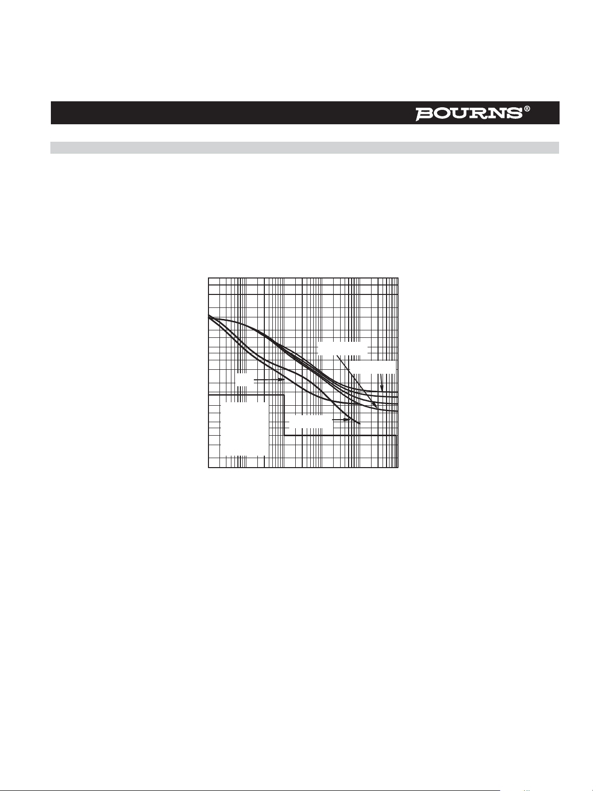
The overcurrent protector should not allow current-time durations greater than the TISP61089B current ratings, otherwise the TISP61089B
may fail. A satisfactory fusible resistor performance is shown in Figure 20. The line feed resistor (LFR) current-time curve is above the first-level
currents and below the TISP61089B rated current for VGG > -100 V. This particular curve is for a Bourns 4B04B-523-400 2 x 40 Ω, 2 %
tolerance, 0.5 % matched resistor module. Fusible resistors are also available with integrated thermal fuses or PTC thermistors. Thermal fuses
will cause a rapid drop in the operating current after about 10 s. Figure 20 shows the fused LFR curve for a Bourns 4B04B-524-400 2 x 40 Ω,
2 % tolerance, 0.5 % matched resistor module with integrated thermal fuse links. The Bourns 4B04B-524-400 allows the TISP61089B to
operate down to its full rated voltage of VGG = -155 V. An LFR with integrated PTC thermistors will give an automatically resettable current
limiting function for all but the highest currents.
PEAK AC
vs
50
CURRENT DURATION
40
30
20
15
10
8
6
5
4
3
2
1.5
1
0.8
0.6
0.5
Peak 50 Hz / 60 Hz Current — A
0.4
0.3
0.2
0.15
0.01 0.1 1 10 100 1000
LFR
First Level
s # 1
Test
through 5,
25 ΩΩΩΩ & 40 Ω
t — Current Duration — s
Ω
ΩΩ
Fused LFR
Figure 20. Line Feed Resistor - with and without Thermal Fuse
V
GG
= -120 V
AI6XDKA
VGG = -60 V
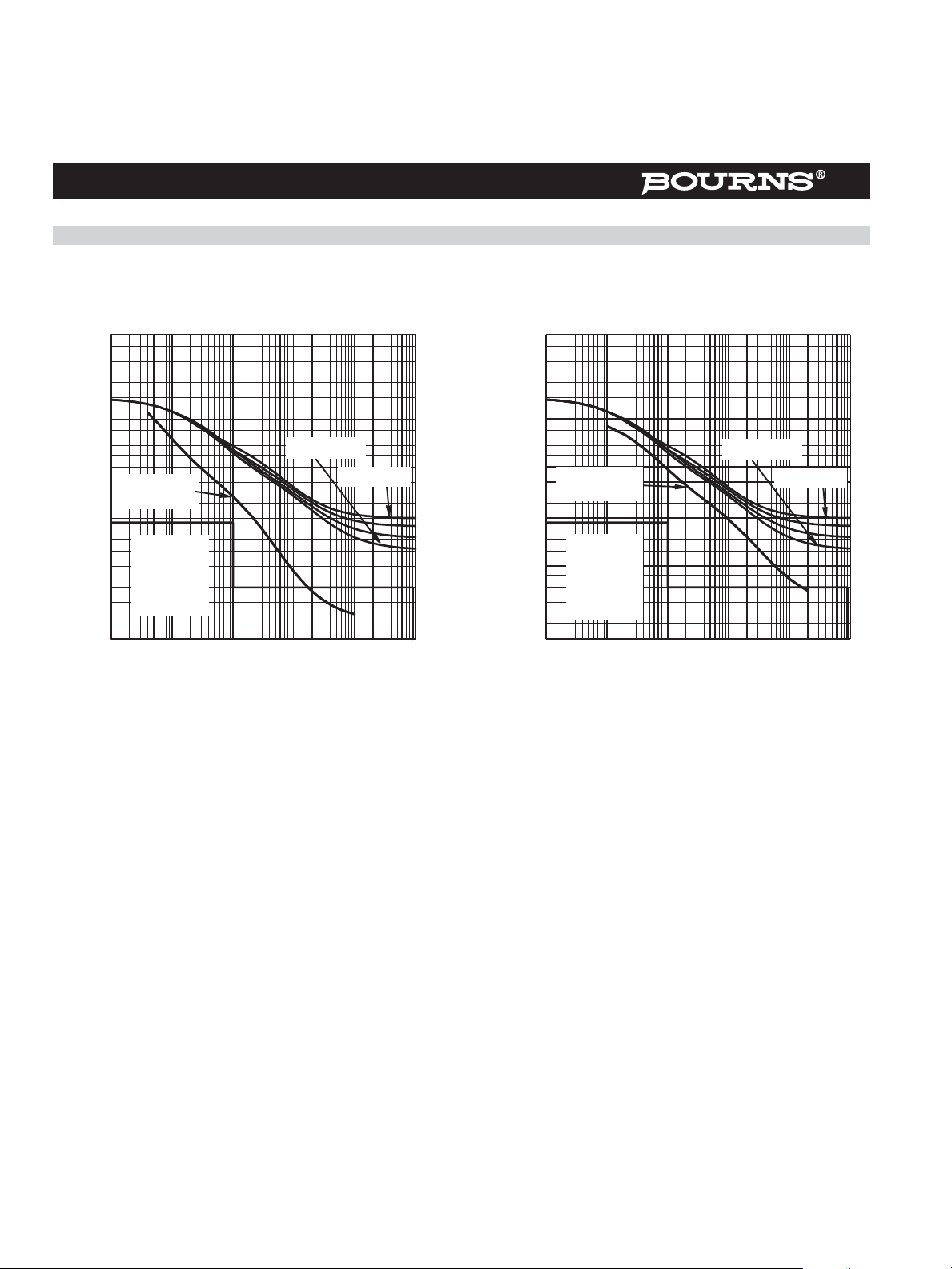
Ceramic PTC thermistors are available in suitable ohmic values to be used as the series line feed resistor RS . Figure 21 overlays a typical
ceramic PTC thermistor operating characteristic. Some of the first-level tests will cause thermistor operation. Generally, the resistance
matching stability of the two PTC thermistors after power fault switching lightning will meet the required line balance performance.
Ceramic PTC thermistors reduce in resistance value under high voltage conditions. Under high current impulse conditions, the resistance can
be less than 50 % of the d.c. resistance. This means that more current than expected will flow under high voltage impulse conditions. The
manufacturer should be consulted on the 2/10 currents conducted by their product under ‘1089 conditions. To keep the 2/10 current below
120 A, an increase of the PTC thermistor d.c. resistance value to 50 Ω or more may be needed. In controlled temperature environments, where
the temperature does not drop below freezing, the TISP61089B 2/10 capability is about 170 A, and this would allow a lower value of
resistance.
Generally, polymer PTC thermistors are not available in sufficiently high ohmic values to be used as the only line feed resistance. To meet the
required resistance value, an addition (fixed) series resistance can be used. Figure 22 overlays a typical polymer PTC thermistor operating
characteristic. Compared to ceramic PTC thermistors, the lower thermal mass of the polymer type will generally give a faster current reduction
time than the ceramic type. However, in this case the polymer resistance value is much less than the ceramic value. For the same current level,
the dissipation in the polymer thermistor is much less than the ceramic thermistor. As a result, the polymer thermistor is slower to operate than
the ceramic one.
The resistance stability of polymer PTC thermistors is not as good as ceramic ones. However, the thermistor resistance change will be diluted
by additional series resistance. If an SLIC with adaptive line balance is used, thermistor resistance stability may not be a problem. Polymer
PTC thermistors do not have a resistance decrease under high voltage conditions.
OCTOBER 2000 - REVISED FEBRUARY 2005
Specifications are subject to change without notice.
Customers should verify actual device performance in their specific applications.
Page 19
TISP61089B High Voltage Ringing SLIC Protector
Overcurrent and Overvoltage Protection Coordination (Continued)
PEAK AC
vs
CURRENT DURATION
50
40
30
20
15
10
8
6
5
4
3
Ceramic PTC
Thermistor
2
1.5
1
First Level
Tests # 1
through 5,
25 ΩΩΩΩ & 40 Ω
0.01 0.1 1 10 100 1000
Ω
ΩΩ
t — Current Duration — s
Peak 50 Hz / 60 Hz Current — A
0.15
0.8
0.6
0.5
0.4
0.3
0.2
Figure 21. Ceramic PTC Thermistor
VGG = -120 V
VGG = -60 V
AI6XDIA
PEAK AC
vs
CURRENT DURATION
50
40
30
20
15
10
8
6
5
4
Polymer PTC
3
Thermistor
2
1.5
1
Fir st Level
Tests # 1
through 5,
25 ΩΩΩΩ & 40 Ω
0.01 0.1 1 10 100 1000
Ω
ΩΩ
t — Current Duration — s
Peak 50 Hz / 60 Hz Current — A
0.15
0.8
0.6
0.5
0.4
0.3
0.2
Figure 22. Polymer PTC Thermistor
V= -120 V
GG
VGG = -60 V
AI6XDJA
OCTOBER 2000 - REVISED FEBRUARY 2005
Customers should verify actual device performance in their specific applications.
Specifications are subject to change without notice.
Page 20
TISP61089B High Voltage Ringing SLIC Protector
MECHANICAL DATA
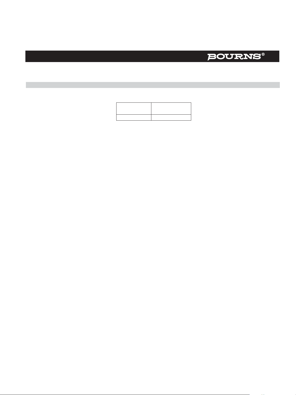
Device Symbolization Code
Devices will be coded as below.
Device
TISP61089B 61089B
Symbolization
Code
OCTOBER 2000 - REVISED FEBRUARY 2005
Specifications are subject to change without notice.
Customers should verify actual device performance in their specific applications.
Page 21
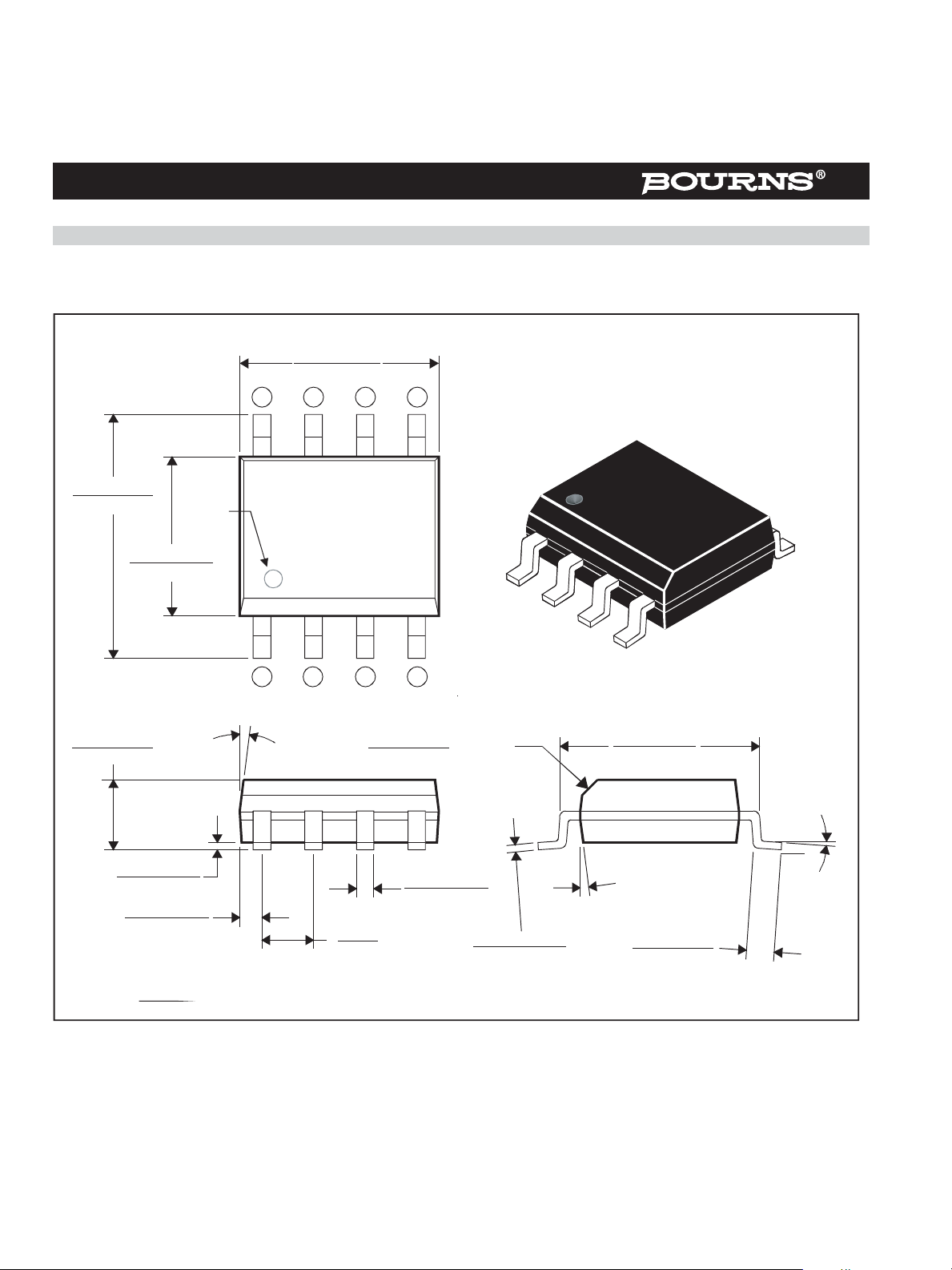
TISP61089B High Voltage Ringing SLIC Protector
D008 Plastic Small-Outline Package
This small-outline package consists of a circuit mounted on a lead frame and encapsulated within a plastic compound. The compound will
withstand soldering temperature with no deformation, and circuit performance characteristics will remain stable when operated in high
humidity conditions. Leads require no additional cleaning or processing when used in soldered assembly.
D008
5. 80 -
(0.228 - 0.244)
(0.053 - 0.069)
6. 20
(0.150 - 0.157)
1. 35 - 1.75
INDEX
3. 81 - 4. 00
(0.189 - 0. 19 7)
8
1
7° NOM
3 Places
4. 80 - 5. 00
765
2
3
4
0. 25 - 0.50
(0.010 - 0.020)
x 45 ° NOM
8-pin Small Outline Microelectronic Standard
Package MS-012, JEDEC Publication 95
4. 60 - 5. 21
(0.181 - 0.205)
0. 10 2 - 0.203
(0.004 - 0.008)
0. 28 - 0.79
(0.011 - 0. 03 1)
DIMENSIONS ARE:
NOTES: A. L eads are within 0.25 (0.010) radius of true position at maximum material condition.
B. Body dimensions do not include mold flash or protrusion.
C. Mold flash or protrusion shall not exceed 0.15 (0.006).
D. Lead tips to be planar within ±0.051 (0.002).
MILLIMETERS
(INCHES)
Pin Spacing
1. 27
(0.050)
(see Note A)
6 Pla ces
0. 36 - 0.51
(0.014 - 0.020)
8 Places
0. 19 0 - 0.229
(0.007 5 - 0.00 90)
Customers should verify actual device performance in their specific applications.
7° NOM
4 Places
0. 51 - 1.12
(0.020 - 0.044)
OCTOBER 2000 - REVISED FEBRUARY 2005
Specifications are subject to change without notice.
4° ± 4°
MDXXAAE
Page 22
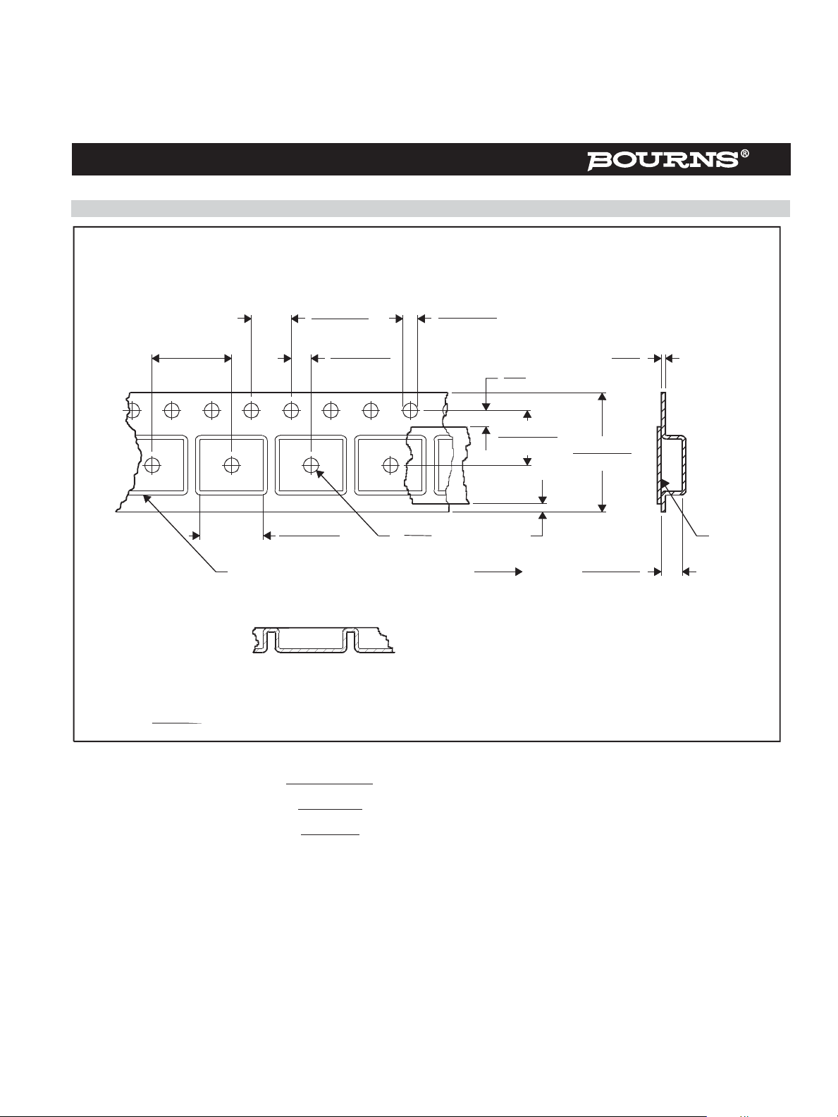
TISP61089B High Voltage Ringing SLIC Protector
D008 - Tape Dimensions
D008 Package (8-pin Small Outline) Single-Sprocket Tape
DIMENSIONS ARE:
7. 90 - 8.10
(.31 1 - .319)
MILLIMETERS
(INCHES)
6. 30 - 6. 50
(.24 8 - .256)
Carrier Tap e
Embos sment
3. 90 -
4.10
(.154 - .161 )
1. 95 - 2.05
(.07 7 - .081)
1. 50 - 1.60
(.059 - .063 )
1. 5
MIN .
(.05 9)
Direction o f Feed
0. 8
MIN .
(.03)
5. 40 - 5. 60
(.213 - .220 )
0 MIN.
(.01 6)
11 .7 0 -
12.30
(.461 - .484 )
2. 0 -
(.079 - .087 )
0. 40
Cover
Tape
2.2
NOTES: A. Ta ped devices are supplied on a reel of the following dimensions:
Reel diameter:
Reel hub diameter:
Reel axial hole:
B. 2500 devices are on a re el.
“TISP” is a trademark of Bourns, Ltd., a Bourns Company, and is Registered in U.S. Patent and Trademark Office.
“Bourns” is a registered trademark of Bourns, Inc. in the U.S. and other countries.
OCTOBER 2000 - REVISED FEBRUARY 2005
Specifications are subject to change without notice.
Customers should verify actual device performance in their specific applications.
33 0 +0. 0/-4 .0
(12.99 +0.0/-.157)
10 0 ±2.0
(3.937 ±.079)
13.0 ±0.2
(.51 2 ±.00 8)
MDXXATC
 Loading...