

Page 1
DUAL-GATE UNIDIRECTIONAL OVERVOLTAGE PROTECTOR
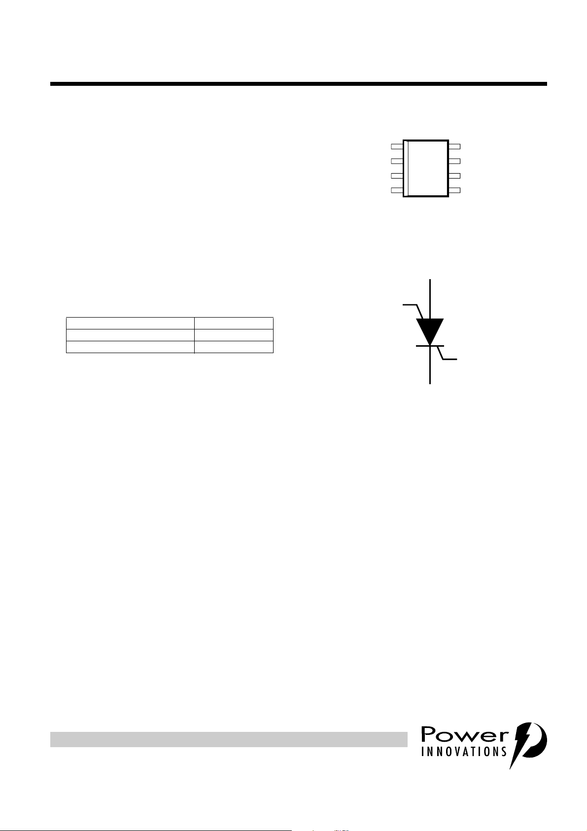
device symbol
K
G1
G2
SD6XAKA
A
OVERVOLTAGE PROTECTION FOR DUAL-VOLTAGE RINGING SLICS
●
Programmable Pr otection Configurations up
to ±100 V
●
Typically 5 Lines Protected by Two
TISP83121D + Diode Steering Networks
●
High Surge Current
- 150 A 10/1000 µs
- 150 A 10/700 µs
- 500 A 8/20 µs
●
Pin compatible with the LCP3121
- Functional Replacement in Diode Steering
Network Applications
- 50% more surge current
●
Small Outline Surface Mount Package
- Available Ordering Options
CARRIER PART #
Tube TISP83121D
Taped and reeled TISP83121DR
TISP83121D
FEBRUARY 1999Copyright © 1999, Power Innovations Limited, UK
D PACKAGE
(TOP VIEW)
1
K
G1
G2
For operation at the rated current values connect
pins 1, 4, 5 and 8 together.
2
3
4
K
8
K
7
A
6
A
5
K
MD6XAYA
description
The TISP83121D is a dual-ga te reverse-blocking
unidirectional thyristor designed for the
protection of dual-voltage ringing SLICs
(Subscriber Line Interface Circuits) against
overvoltages on the telephone line caused by
lightning, a.c. power contact and induction.
The device chip is a four-layer NPNP silicon
thyristor structure which has an electrode
connection to every layer. For negative
overvoltage protection the TISP83121D is used
in a common anode configuration with the
voltage to be limited applied to the cathod e (K)
terminal and the negative reference potential
applied to the gate 1 (G1 ) terminal. For positive
overvoltage protection the TISP83121D is used
in a common cathode configuration with the
voltage to be limited applied to the anode (A)
terminal and the positive reference potential
applied to the gate 2 (G2) terminal.
The TISP83121D is a unidirectional protector
and to prevent reverse bias, requires the use of a
series diode between the protected line
conductor and the protector. Further, the gate
reference supply voltage requires an
appropriately poled series diode to prevent the
supply from being shorted when the
TISP83121D crowbars.
Under low level power cross conditions the
TISP83121D gate current will charge the gate
reference supply. If the reference su pply cannot
absorb the charging current its potential will
increase, possibly to damaging levels. To avoid
excessive voltage levels a clamp (zener or
avalanche breakdown diode) may be added in
shunt with the supply. Alternatively, a grounded
collector emitter -follower may be used to reduce
the charging current by the transistors H
value.
FE
This monolithic protection device is mad e with a
ion-implanted epi taxial-planar tech nology to give
a consistent protection performance and be
virtually transparent to the system in normal
operation.
PRODUCT INFORMATION
Information is current as of publication date. Produc ts conform to specifications in accordance
with the terms of Power Innovations standard warranty. Production processing does not
necessarily include testing of all parameters.
1
Page 2

TISP83121D
DUAL-GATE UNIDIRECTIONAL OVERVOLTAGE PROTECTOR
FEBRUA RY 1999
absolute maximum ratings
RATING SYMBOL VALUE UNIT
Repetitive peak off-state voltage, 0 °C to 70 °C V
Non-repetitive peak on-state pulse current (see Notes 1 and 2)
10/1000 µs (GR-1089-CORE, open-circuit voltage wave shape 10/1000 µs) 150
5/310 µs (CCITT K20/21, open-circuit voltage wave shape 7 kV10/700 µs) 150
8/20 µs (ANSI C62.41, open-circuit voltage wave shape 1.2/50 µs) 500
Non-repetitive peak on-state current, 50 Hz, halfwave rectified sinewave, (see Notes 1 and 2)
100 ms
1 s
900 s
Junction temperature T
Storage temperature range T
I
I
TSM
DRM
TSP
J
stg
100 V
22
8
3
-40 to +150 °C
-65 to +150 °C
A
A
NOTES: 1. Initially the protector must be in thermal equilibrium with 0 °C < T
its initial conditions. For operation at the rated current value, pins 1, 4, 5 and 8 must be connected together.
< 70 °C. The surge may be repeated after the device returns to
J
2. Above 70 °C, derate linearly to zero at 150 °C lead temperature.
electrical characteristics, TJ = 25 °C (unless otherwise noted)
PARAMETER TEST CONDITIONS MIN TYP MAX UNIT
Off-state current Vd=70V, IG=0 1µA
I
D
Repetitive peak off-state
I
DRM
current
Holding current IT= 1 A, di/dt = -1A/ms
I
H
Reverse current VR=0.3V 1mA
I
R
I
Gate G1 trigger current IT=+1A, t
G1T
Gate G2 trigger current IT=+1A, t
I
G2T
G1-K trigger voltage IT=+1A, t
V
G1T
G2-A trigger voltage IT=+1A, t
V
G2T
Anode to cathode off-
C
AK
state capacitance
V
d=VDRM
f=1MHz, V
= 100 V, IG= 0, 0 °C to 70 °C 10 µA
T
= 0 to 70 °C
J
= 25 °C
T
J
= 70 °C
T
J
= 20 µs +200 mA
p(g)
= 20 µs -180 mA
p(g)
=20µs +1.8 V
p(g)
=20µs -1.8 V
p(g)
=1V
d
, VD=5V, IG= 0 (see Note 3) 100 pF
RMS
90
60
300
mA
NOTE 3: These capacitance measurements employ a three terminal capacitance bridge incor porating a guard circuit. The unmeasured
device terminals are decoupled to the guard terminal of the bridge.
thermal characterist ics
PARAMETER TEST CONDITIONS MIN TYP MAX UNIT
R
Junction to free air thermal resistance
θ
JA
PRODUCT INFORMATION
2
= 25 °C, EIA/JESD51-3 PCB,
T
A
EIA/JESD51-2 environment, I
= I
T
TSM(900)
105 °C/W
Page 3
DUAL-GATE UNIDIRECTIONAL OVERVOLTAGE PROTECTOR
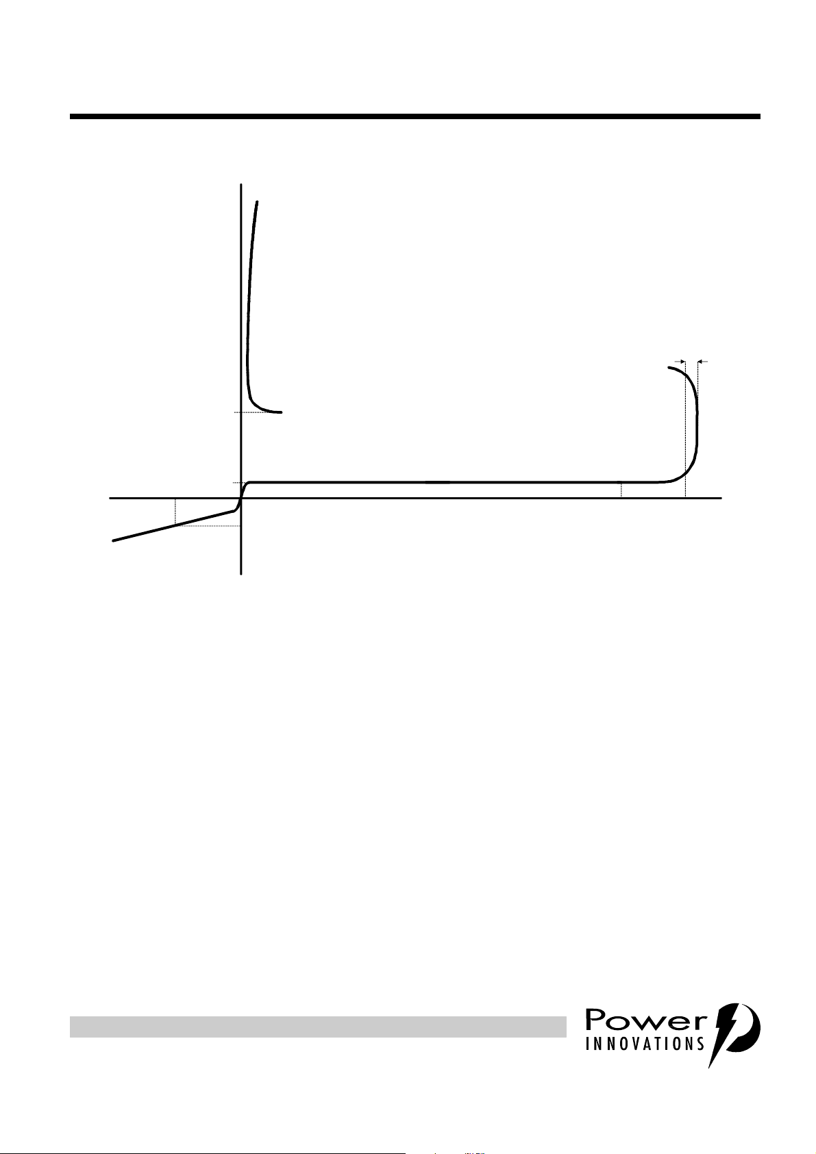
PARAMETER MEASUREMENT INFORMATION
+i
I
H
TISP83121D
FEBRUARY 1999
QUADRANT 1
ANODE POSITIVE
SWITCHING CHARACTERISTIC
V
GT
I
V
-v
QUADRANT III
ANODE NEGATIVE
REVERSE CHARACTERISTIC
R
D
V
I
R
-i
DRM
REFERENCE
VOLTAGE
Figure 1. VOLTAGE-CURRENT CHARACTERISTIC
multiple line overvoltage protectio n
Figure 2 shows two TISP83121D devices protecting many lines. Line conductor positive overvoltage
protection is given by the steering diode ar ray connected to the anode of the upper TISP83121D and the
TISP83121D itself. The TISP83 121D gate reference voltage is the positive batter y supply, +V
limiting voltage will be the sum of the voltages of the batter y, th e forward biased conductor diode, the gate
trigger of the TISP8312 1D and the forward biased reference voltage blocking diode. Typic ally the conductor
voltage will be initially limited at 2.5 V above the +V
BAT
value.
Line conductor negative overvoltage protecti on i s given by the diode ste ering array connected to the cathode
of the lower TISP83121D and the TISP83121D itself. The TISP83121D gate reference voltage is the negative
battery sup ply, -V
. The initial limiting voltage wil l be the sum of the voltages of the batter y, the forward
BAT
biased conductor diode, the gate trigger of the TISP83121D and the forward biased reference voltage
blocking diode. Typically the conductor voltage will be initially limited at 2.5 V below the -V
When an TISP83121D crowbars and grounds all conductors of the appropriate polarity, the device current will
be the sum of all the SLIC output currents. This will usually exceed the TISP83121D holding current. To
switch off the TISP83121D and re sto re normal operation , the grou nde d cond iti on of the SLIC output must be
detected and the SLIC outputs turned off.
BAT
BAT
value.
+v
PM6XAGB
. The initial
The 150 A rating of the TISP83121D a llows a large number of li nes to be prot ected agains t currents cau sed
by lightning. For example, if a recommendation K.20 10 /700 generator was connected to all lines, together
PRODUCT INFORMATION
3
Page 4

TISP83121D
DUAL-GATE UNIDIRECTIONAL OVERVOLTAGE PROTECTOR
FEBRUA RY 1999
R1
R
LINE 1
IN
R
T1
SLIC 1
A
G2
+VE
REFERENCE
VOLTAGE
+V
BAT
RN
LINE N
IN
TN
G1
R
R
R
R
SLIC N
TISP83121D
K
G2
TISP83121D
A
G1
K
-VE
REFERENCE
VOLTAGE
Figure 2. N LINE POSITIVE AND NEGATIVE OVERVOLTAGE PROTECTION
A
A
G2
+VE
REFERENCE
VOLTAGE
+V
BAT
G1
G2
REFERENCE
VOLTAGE
0
-V
BAT
AI8XAA
+VE
+V
BAT
TISP83121D
A
G2
K
TISP83121D
G1
K
REFERENCE
VOLTAGE
(B)
-VE
0
-V
BAT
AI8XAB
G2
G1
A
TISP83121D
K
TISP83121D
G1
K
REFERENCE
(A)
-VE
VOLTAGE
0
-V
BAT
Figure 3. REFERENCE VOLTAGE CONTROL BY (A) BREAKDOWN DIODES
OR (B) BY TRANSISTOR BUFFERS
with 350 V primary protection and a series conductor resistance (R) of 25Ω, the maximum conductor current
before the primar y protection ope rated would be 350/25 = 14 A or 28 A per line. For a total return current of
about 150 A the number of lines would be 150/28 = 5. At this current level, 5x28 = 140 A, the generator
PRODUCT INFORMATION
4
Page 5

TISP83121D
DUAL-GATE UNIDIRECTIONAL OVERVOLTAGE PROTECTOR
FEBRUARY 1999
voltage would be 140((25+25)/10+ 15) = 2 800 V. Another limitation is lon g term power cross. The long ter m
power cross capability of the TISP83121D is 3 A peak or 2.1 A rms. If the line conductor overcurrent
protection was given by a PTC resistor which switched at 0.2 A, the maximum number of conductors
becomes 2.1/0.2 = 10 or 5 lines.
battery supply impedance
In many designs, the batter y supply voltages are generated by switching mode power suppli es. This type of
power supply cannot be charged like a battery. Feeding a charging current to a switching mode power supply
will usually cause the supply to stop switching and the voltage to rise. The gate current of the TISP83121D is
a charging current for the supply. To avoid the supply voltage from rising and damaging the connected SLICs,
an avalanche diode voltage clamp can be connected across the supply (Figure 3. (A)).
Another approach is to reduce the gate charging current for the supply by a transistor buffer (Figure 3. (B)). If
the transistor gain was 50, a 200 mA gate current would be reduced to a supply charging current of
200/50 = 4 mA In both cases, the dissipatio n in the contr ol devices can be su bstantial an d power capability
needs to be taken into account in device selection.
PRODUCT INFORMATION
5
Page 6

TISP83121D
DUAL-GATE UNIDIRECTIONAL OVERVOLTAGE PROTECTOR
FEBRUA RY 1999
MECHANICAL DATA
D008
plastic small-outline package
This small-outline pa ckage consists of a circuit mo unted on a lead frame an d encapsulated with in a plastic
compound. The compound will withstand soldering temperature with no deformation, and circuit performance
characteristics will remain stable when operated in high humidity conditions. Leads require no additional
cleaning or processing when used in soldered assembly.
D008
6,20 (0.244)
5,80 (0.228)
1,75 (0.069)
1,35 (0.053)
4,00 (0.157)
3,81 (0.150)
8
1
7° NOM
3 Places
5,00 (0.197)
4,80 (0.189)
765
432
0,50 (0.020)
0,25 (0.010)
x 45°NOM
Designation per JEDEC Std 30:
PDSO-G8
5,21 (0.205)
4,60 (0.181)
0,203 (0.008)
0,102 (0.004)
0,79 (0.031)
0,28 (0.011)
ALL LINEAR DIMENSIONS ARE IN MILLIMETERS AND PARENTHETICALLY IN INCHES
NOTES: A. Leads are within 0,25 (0.010) radius of true position at maximum material condition.
B. Body dimensions do not include mold flash or protrusion.
C. Mold flash or protrusion shall not exceed 0,15 (0.006).
D. Lead tips to be planar within ±0,051 (0.002).
Pin Spacing
1,27 (0.050)
(see Note A)
6 Places
0,51 (0.020)
0,36 (0.014)
8 Places
0,229 (0.0090)
0,190 (0.0075)
PRODUCT INFORMATION
6
7° NOM
4 Places
1,12 (0.044)
0,51 (0.020)
4° ± 4°
MDXXAA
Page 7

TISP83121D
DUAL-GATE UNIDIRECTIONAL OVERVOLTAGE PROTECTOR
FEBRUARY 1999
IMPORTANT NOTICE
Power Innovations Limited (PI) reserves the right to make changes to its products or to discontinue any semiconductor product
or service without notice, and advises its customers to verify, before placing orders, that the information being relied on is
current.
PI warrants performance of its semiconductor products to the specifications applicable at the time of sale in accordance with
PI's standard wa rranty. Tes ting and o ther qu ali ty contr ol techn iques are u tilis ed to the e xtent PI deem s n ecessary t o support this
warranty. Specific testing of all param eters of ea ch devi ce is not nec essa rily perf ormed, except those mandate d by gove rnment
requirements.
PI assumes no liability for applications assistance, customer product design, software performance, or infringement of patents
or services described herein. Nor is any license, either express or implied, granted under any patent right, copyright, design
right, or other intellectual property right of PI covering or relating to any combination, machine, or process in which such
semiconductor products or services might be or are used.
PI SEMICONDUCTOR PRODUCTS ARE NOT DESIGNED, INTENDED, AUTHORISED, OR WARRANTED TO BE SUITABLE
FOR USE IN LIFE-SUPPORT APPLICATIONS, DEVICES OR SYSTEMS.
Copyright © 1999, Power Innovations Limited
PRODUCT INFORMATION
7
 Loading...