

Page 1
TISP61511D, TISP61512P
DUAL FORWARD-CONDUCTING P-GATE THYRISTORS
PROGRAMMABLE OVERVOLTAGE PROTECTORS
PRODUCT INFORMATION
1
JULY 1995 - REVISED SEPTEMBER 1997Copyright © 1997, Power Innovations Limited, UK
Information is current as of publication date. Products conform to specifications in accordance
with the terms of Power Innovations standard warranty. Production processing does not
necessarily include testing of all parameters.
PROGRAMMABLE SLIC OVERVOLTAGE PROTECTION
from 0 V (ground) and a negative voltage in the region of -10 V to -70 V. The protector gate is connected to
this negative supply. This references the protection (clipping) voltage to the negative supply voltage. As the
protection voltage will track the negative supply voltage the overvoltage stress on the SLIC is minimised.
Positive overvoltages are clipped to ground by diode forward conduction. Negative overvoltages are initially
clipped close to the SLIC negative supply rail value. If sufficient current is available from the overvoltage, then
the protector will crowbar into a low voltage on-state condition. As the current subsides the high holding
current of the crowbar prevents d.c. latchup.
These monolithic protection devices are fabricated in ion-implanted planar vertical power structures for high
reliability and in normal system operation they are virtually transparent. The buffered gate design reduces the
loading on the SLIC supply during overvoltages caused by power cross and induction.
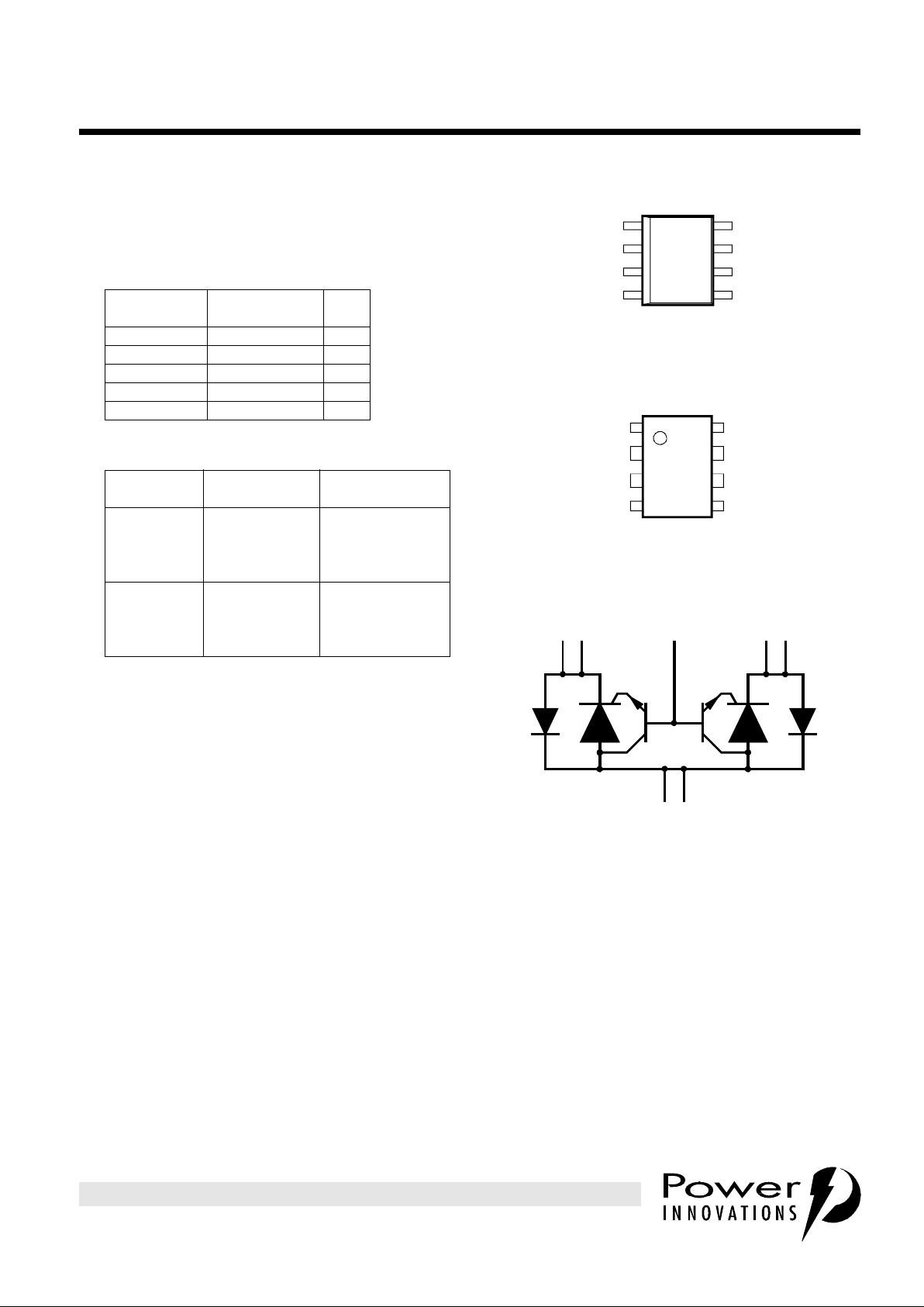
● Dual Voltage-Programmable Protectors.
- Wide 0 to -80 V Programming Range
- Low 5 mA max. Triggering Current
- High 150 mA min. Holding Current
● Rated for International Surge Wave Shapes
● Functional Replacements for
description
The TISP61511D and TISP61512P are dual
forward-conducting buffered p-gate overvoltage
protectors. They are designed to protect
monolithic Subscriber Line Interface Circuits,
SLICs, against overvoltages on the telephone
line caused by lightning, ac power contact and
induction. The TISP61511D and TISP61512P
limit voltages that exceed the SLIC supply rail
voltage.
The SLIC line driver section is typically powered
VOLTAGE
WAVE SHAPE
STANDARD
I
TSP
A
2/10 µs TR-NWT-001089 170
1.2/50 µs ETS 300 047-1 90
0.5/700 µs RLM88/I3124 40
10/700 µs K17, K20, K21 40
10/1000 µs TR-NWT-001089 30
DEVICE TYPE PACKAGE TYPE
FUNCTIONAL
REPLACEMENT
LCP1511,
LCP1511D,
ATTL7591AS,
MGSS150-1
8-pin Small-Outline
TISP61511D
or order as
TISP61511DR
for Taped and Reeled
LCP1512,
LCP1512D,
ATTL7591AB,
MGSS150-2
8-pin Plastic DIP TISP61512P
device symbol
Terminals K1, K2 and A correspond to the alternative
line designators of T, R and G or A, B and C. The
negative protection voltage is controlled by the voltage,
V
GG,
applied to the G terminal.
SD6XAE
A
K1 G K2
MD6XAJ
'61512P PACKAGE
(TOP VIEW)
NC - No internal connection
Terminal typical application names shown in
parenthesis
1
2
3
4
5
6
7
8
K2
G
K1
NC
K1
A
A
K2
(Tip)
(Ground)
(Ground)
(Ring)
(Gate)
(Tip)
(Ring)
MD6XAL
'61511D PACKAGE
(TOP VIEW)
NC - No internal connection
Terminal typical application names shown in
parenthesis
1
2
3
4
5
6
7
8
K1
A
A
K2
G
K1
K2
NC
(Tip)
(Ground)
(Ground)
(Ring)
(Gate)
(Tip)
(Ring)
Page 2

TISP61511D, TISP61512P
DUAL FORWARD-CONDUCTING P-GATE THYRISTORS
PROGRAMMABLE OVERVOLTAGE PROTECTORS
2
JULY 1995 - REVISED SEPTEMBER 1997
PRODUCT INFORMATION
NOTES: 1. Initially the protector must be in thermal equilibrium with -40°C ≤ TJ≤ 85°C, unless otherwise specified. The surge may be
repeated after the device returns to its initial conditions. See the applications section for the details of the impulse generators.
2. The rated current values may be applied to either the R-G or T-G terminal pairs. Additionally, both terminal pairs may have their
rated current values applied simultaneously (in this case the G terminal current will be twice the rated current value of an individual
terminal pair). Above 85°C, derate linearly to zero at 150°C lead temperature.
absolute maximum ratings
RATING SYMBOL VALUE UNIT
Repetitive peak off-state voltage, I
G
= 0, -40°C ≤ TJ≤ 85°C V
DRM
-100 V
Repetitive peak gate-cathode voltage, V
KA
= 0, -40°C ≤ TJ≤ 85°C V
GKRM
-85 V
Non-repetitive peak on-state pulse current(see Notes 1 and 2)
I
TSP
A
10/1000 µs 30
5/310 µs
0.2/310 µs
40
40
1/20 µs
2/10 µs T
J
= -40°C
T
J
= 25, 85°C
90
120
170
Non-repetitive peak on-state current, 50 Hz (see Notes 1 and 2)
I
TSM
A full-sine-wave, 20 ms 5
1 s 3.5
Non-repetitive peak gate current, half-sine-wave, 10 ms (see Notes 1 and 2) I
GSM
2 A
Junction temperature T
J
-55 to +150 °C
Storage temperature range T
stg
-55 to +150 °C
recommended operating conditions
MIN TYP MAX UNIT
C
G
Gate decoupling capacitor 220 nF
electrical characteristics, TJ = 25°C (unless otherwise noted)
PARAMETER TEST CONDITIONS MIN TYP MAX UNIT
I
D
Off-state current VD= -85 V, VGK= 0 V
T
J
= 25°C 5 µA
T
J
= 70°C 50 µA
V
(BO)
Breakover voltage IT= 30 A, 10/1000 µs, 1 kV, RS= 33 Ω, di/dt
(i)
= 8 A/µs (see Note 3) -58 V
V
GK(BO)
Gate-cathode voltage
at breakover
I
T
= 30 A, 10/700 µs, 1.5 kV, RS= 10 Ω, di/dt
(i)
= 14 A/µs (see Note 3)
I
T
= 30 A, 1.2/50 µs, 1.5 kV, RS= 10 Ω, di/dt
(i)
= 70 A/µs (see Note 3)
I
T
= 38 A, 2/10 µs, 2.5 kV, RS= 61 Ω, di/dt
(i)
= 40 A/µs (see Note 3)
10
20
25
V
V
T
On-state voltage
I
T
= 0.5 A, tw= 500 µs
I
T
= 3 A, tw= 500 µs
3
4
V
V
F
Forward voltage IF= 5 A, tw= 500 µs 3 V
V
FRM
Peak forward recovery
voltage
I
F
= 30 A, 10/1000 µs, 1 kV, RS= 33 Ω, di/dt
(i)
= 8 A/µs (see Note 3)
I
T
= 30 A, 10/700 µs, 1.5 kV, RS= 10 Ω, di/dt
(i)
= 14 A/µs (see Note 3)
I
T
= 30 A, 1.2/50 µs, 1.5 kV, RS= 10 Ω, di/dt
(i)
= 70 A/µs (see Note 3)
I
T
= 38 A, 2/10 µs, 2.5 kV, RS= 61 Ω, di/dt
(i)
= 40 A/µs (see Note 3)
5
5
7
12
V
I
H
Holding current IT= 1 A, di/dt = -1A/ms, VGG= -48 V 150 mA
I
GAS
Gate reverse current VGG= -75 V, K and A terminals connected
T
J
= 25°C 5 µA
T
J
= 70°C 50 µA
I
GT
Gate trigger current IT= 3 A, t
p(g)
≥ 20 µs, VGG= -48 V 0.2 5 mA
V
GT
Gate trigger voltage IT= 3 A, t
p(g)
≥ 20 µs, VGG= -48 V 2.5 V
NOTE 3: All tests have C
G
= 220 nF and VGG = -48 V. RS is the current limiting resistor between the output of the impulse generator and
the R or T terminal. See the applications section for the details of the impulse generators.
Page 3
3
JULY 1995 - REVISED SEPTEMBER 1997
TISP61511D, TISP61512P
DUAL FORWARD-CONDUCTING P-GATE THYRISTORS
PROGRAMMABLE OVERVOLTAGE PROTECTORS
PRODUCT INFORMATION
C
AK
Anode-cathode offstate capacitance
f = 1 MHz, V
d
= 1 V, IG= 0, (see Note 4)
V
D
= -3 V 100 pF
V
D
= -48 V 50 pF
NOTE 4: These capacitance measurements employ a three terminal capacitance bridge incorporating a guard circuit. The unmeasured
device terminals are a.c. connected to the guard terminal of the bridge.
thermal characteristics
PARAMETER
TEST CONDITIONS
MIN TYP MAX UNIT
R
θJA
Junction to free air thermal resistance
P
tot
= 0.8 W,TA= 25°C
5 cm
2
, FR4 PCB
D Package 170
°C/W
P Package 125
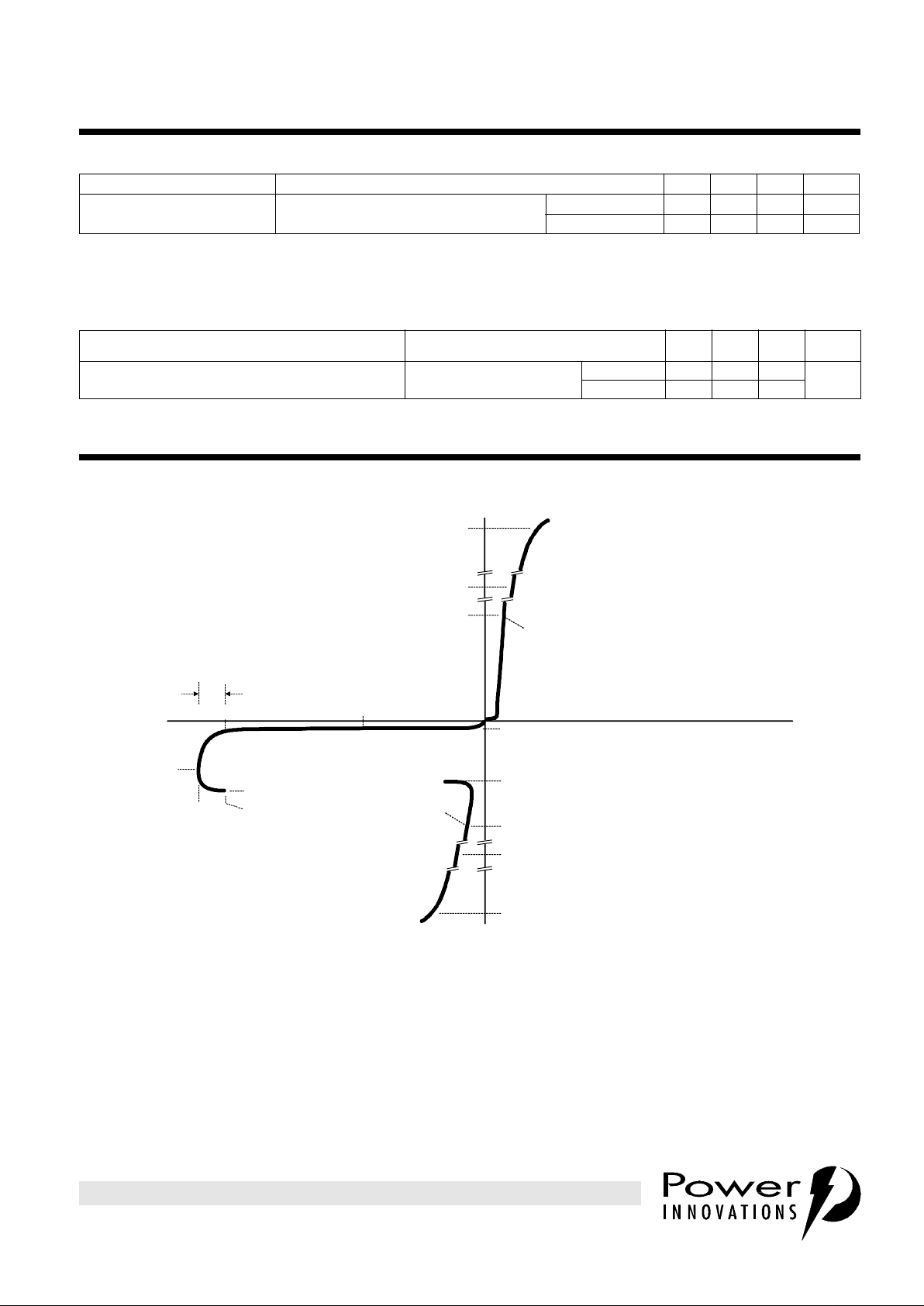
PARAMETER MEASUREMENT INFORMATION
Figure 1. VOLTAGE-CURRENT CHARACTERISTIC
electrical characteristics, TJ = 25°C (unless otherwise noted) (Continued)
PARAMETER TEST CONDITIONS MIN TYP MAX UNIT
-v
I
S
V
S
V
GG
V
D
I
H
I
T
V
T
I
TSM
I
TSP
V
(BO)
I
(BO)
I
D
Quadrant I
Forward
Conduction
Characteristic
+v
+i
I
F
V
F
I
FSM
(= |I
TSM
|)
I
FSP
(= |I
TSP
|)
-i
Quadrant III
Switching
Characteristic
PM6XAAA
V
GK(BO)
Page 4
TISP61511D, TISP61512P
DUAL FORWARD-CONDUCTING P-GATE THYRISTORS
PROGRAMMABLE OVERVOLTAGE PROTECTORS
4
JULY 1995 - REVISED SEPTEMBER 1997
PRODUCT INFORMATION
DEVICE PARAMETERS
general
Thyristor based overvoltage protectors, for telecommunications equipment, became popular in the late
1970s. These were fixed voltage breakover triggered devices, likened to solid state gas discharge tubes. As
these were new forms of thyristor, the existing thyristor terminology did not cover their special characteristics.
This resulted in the invention of new terms based on the application usage and device characteristic. Initially,
there was a wide diversity of terms to describe the same thing, but today the number of terms have reduced
and stabilised.
Programmable, (gated), overvoltage protectors are relatively new and require additional parameters to
specify their operation. Similarly to the fixed voltage protectors, the introduction of these devices has resulted
in a wide diversity of terms to describe the same thing. To help promote an understanding of the terms and
their alternatives, this section has a list of alternative terms and the parameter definitions used for this data
sheet. In general, the Texas Instruments approach is to use terms related to the device internal structure,
rather than its application usage as a single device may have many applications each using a different
terminology for circuit connection.
alternative symbol cross-reference guide
This guide is intended to help the translation of alternative symbols to those used in this data sheet. As in
some cases the alternative symbols have no substance in international standards and are not fully defined by
the originators, users must confirm symbol equivalence. No liability will be assumed from the use of this
guide.
THERMAL INFORMATION
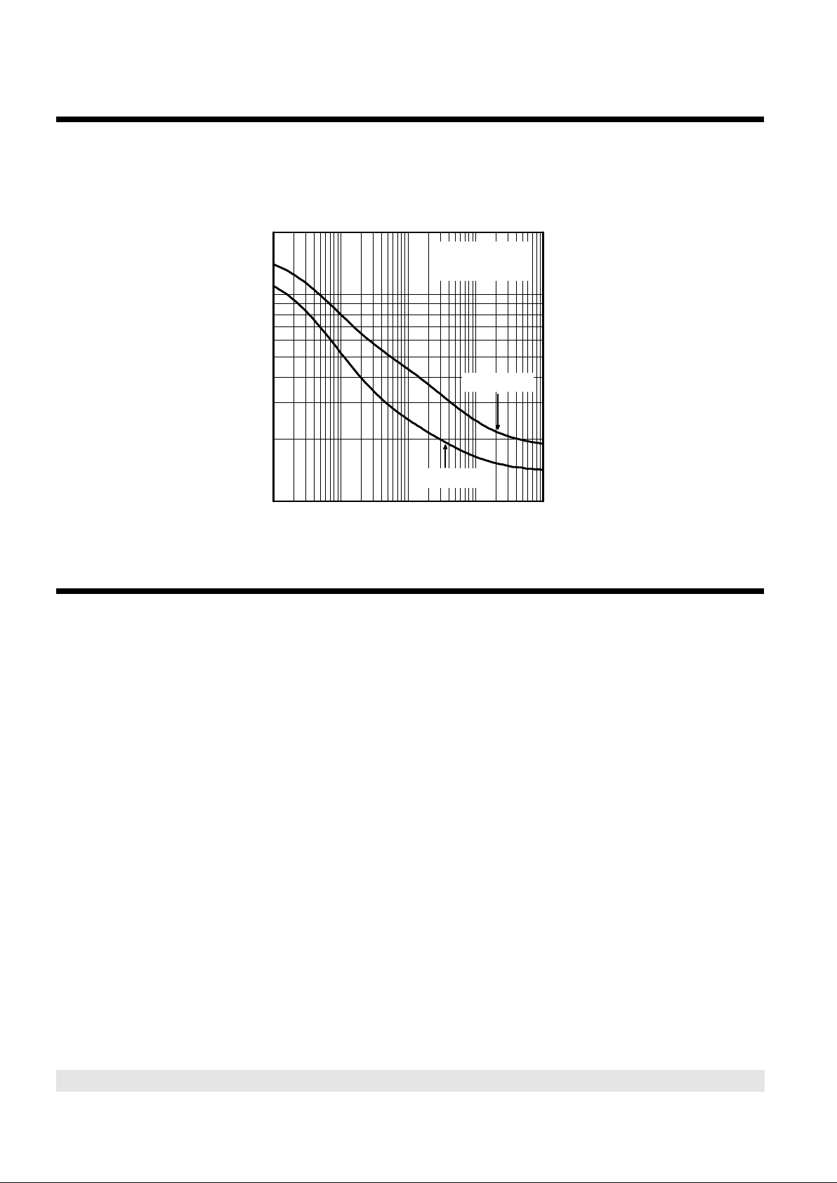
Figure 2.
MAXIMUM NON-RECURRING 50 Hz CURRENT
t - Current Duration - s
0·1 1 10 100 1000
I
TRMS
- Maximum Non-Recurrent 50 Hz Current - A
1
10
vs
CURRENT DURATION
TI6LAA
V
GEN
= 250 Vrms
R
GEN
= 10 to 150 Ω Ω
TISP61511D
TISP61512P
Page 5

5
JULY 1995 - REVISED SEPTEMBER 1997
TISP61511D, TISP61512P
DUAL FORWARD-CONDUCTING P-GATE THYRISTORS
PROGRAMMABLE OVERVOLTAGE PROTECTORS
PRODUCT INFORMATION
APPLICATIONS INFORMATION
electrical characteristics
The electrical characteristics of a thyristor overvoltage protector are strongly dependent on junction
temperature, T
J
. Hence a characteristic value will depend on the junction temperature at the instant of
measurement. The values given in this data sheet were measured on commercial testers, which generally
minimise the temperature rise caused by testing.
application circuit
Figure 3 shows a typical TISP6151xx SLIC card protection circuit. The incoming line wires, R and T, connect
to the relay matrix via the series over-current protection. Fusible resistors, fuses and positive temperature
coefficient (PTC) resistors can be used for over-current protection. Resistors will reduce the prospective
current from the surge generator for both the TISP6151xx and the ring/test protector. The TISP7xxxF3
protector has the same protection voltage for any terminal pair. This protector is used when the ring generator
configuration maybe ground or battery-backed. For dedicated ground-backed ringing generators, the
TISP3xxxF3 gives better protection as its inter-wire protection voltage is twice the wire to ground value.
Relay contacts 3a and 3b connect the line wires to the SLIC via the TISP6151xx protector. The protector gate
reference voltage comes from the SLIC negative supply (V
BAT
). A 220 nF gate capacitor sources the high
gate current pulses caused by fast rising impulses.
TISP61511D, TISP61512P PARAMETER
DATA SHEET
SYMBOL
ALTERNATIVE
SYMBOL
ALTERNATIVE PARAMETER
Non-repetitive peak on-state pulse current I
TSP
I
PP
Peak pulse current
Off-state current I
D
I
R
I
RM
Reverse leakage current LINE/GND
Gate reverse current (with A and K terminals connected) I
GAS
I
RG
Reverse leakage current GATE/LINE
Off-state voltage V
D
V
R
V
RM
Reverse voltage LINE/GND
Peak forward recovery voltage V
FRM
V
FP
Peak forward voltage LINE/GND
Breakover voltage V
(BO)
V
SGL
Dynamic switching voltage GND/LINE
Gate voltage, (V
GG
is gate supply voltage referenced
to the A terminal)
V
G
V
gate
V
GATE
V
S
GATE/GND voltage
Repetitive peak off-state voltage V
DRM
V
MLG
Maximum voltage LINE/GND
Repetitive peak gate-cathode voltage V
GKM
V
MGL
Maximum voltage GATE/LINE
Gate-cathode voltage V
GK
V
GL
GATE/LINE voltage
Gate-cathode voltage at breakover V
GK(BO)
V
DGL
Dynamic switching voltage GATE/LINE
Cathode-anode voltage V
K
V
LG
V
GND/LINE
LINE/GND voltage
Anode-cathode capacitance C
AK
C
off
Off-state capacitance LINE/GND
Cathode 1 terminal K1 Tip Tip terminal
Cathode 2 terminal K2 Ring Ring terminal
Anode terminal A GND Ground terminal
Gate terminal G Gate Gate terminal
Thermal Resistance, junction to ambient R
θJA
Rth (j-a) Thermal Resistance, junction to ambient
Page 6

TISP61511D, TISP61512P
DUAL FORWARD-CONDUCTING P-GATE THYRISTORS
PROGRAMMABLE OVERVOLTAGE PROTECTORS
6
JULY 1995 - REVISED SEPTEMBER 1997
PRODUCT INFORMATION
impulse conditions
Most lightning tests, used for equipment verification, specify a unidirectional sawtooth waveform which has an
exponential rise and an exponential decay. Wave shapes are classified in terms of Peak Amplitude (voltage or
current), rise time and a decay time to 50% of the maximum amplitude. The notation used for the wave shape
is amplitude, rise time/decay time. A 38 A, 5/310 µs wave shape would have a peak current value of 38 A, a
rise time of 5 µs and a decay time of 310 µs.
There are three categories of surge generator type, single wave shape, combination wave shape and circuit
defined. Single wave shape generators have essentially the same waveshape for the open circuit voltage and
short circuit current (e.g. 10/1000 µs open circuit voltage and short circuit current). Combination generators
have two wave shapes, one for the open circuit voltage and the other for the short circuit current (e.g.
1.2/50 µs open circuit voltage and 8/20 µs short circuit current). Circuit specified generators usually equate to
a combination generator, although typically only the open circuit voltage waveshape is referenced (e.g. a
10/700 µs open circuit voltage generator typically produces a 5/310 µs short circuit current). If the
combination or circuit defined generators operate into a finite resistance the wave shape produced is
intermediate between the open circuit and short circuit values.
When the TISP switches into the on-state it has a very low impedance. As a result, although the surge wave
shape may be defined in terms of open circuit voltage, it is the current waveshape that must be used to
assess the TISP surge requirement. As an example, the CCITT IX K17 1.5 kV, 10/700 µs surge is changed to
a 38 A 5/310 µs waveshape when driving into a short circuit. The impulse generators used for rated values
are tabulated below
Figure 3. TYPICAL APPLICATION CIRCUIT
IMPULSE GENERATORS USED FOR RATED VALUES
STANDARD
PEAK
VOLTAGE
SETTING
V
VOLTAGE
WAVE
FORM
µs
GENERATOR
FICTIVE SOURCE
IMPEDANCE
Ω
EXTERNAL
SERIES
RESISTANCE
Ω
PEAK
CURRENT
A
CURRENT
WAVE
FORM
µs
TR-NWT-001089 2500 2/10 5 10 170 2/10
TEST
RELAY
RING
RELAY
SLIC
RELAY
TEST
EQUIP-
MENT
RING
GENERATOR
S1a
S1b
R1a
R1b
RING
WIRE
TIP
WIRE
Th1
Th2
Th3
Th4
Th5
SLIC
SLIC
PROTECTOR
RING/TEST
PROTECTION
OVER-
CURRENT
PROTECTION
S2a
S2b
TISP
6151xx
TISP
3xxxF3
OR
7xxxF3
S3a
S3b
V
BAT
220 nF
AI6XAA
Page 7

7
JULY 1995 - REVISED SEPTEMBER 1997
TISP61511D, TISP61512P
DUAL FORWARD-CONDUCTING P-GATE THYRISTORS
PROGRAMMABLE OVERVOLTAGE PROTECTORS
PRODUCT INFORMATION
Figures 4. and 5. show how the TISP6151xx limits negative and positive over-voltages. Negative overvoltages
(Figure 4.) are initially clipped close to the SLIC negative supply rail value (V
BAT
). If sufficient current is
available from the overvoltage, then the protector (Th5) will crowbar into a low voltage on-state condition. As
the overvoltage subsides the high holding current of the crowbar prevents dc latchup. The protection voltage
will be the sum of the gate supply (V
BAT
) and the peak gate-cathode voltage (V
GK(BO)
). The protection voltage
will be increased if there is a long connection between the gate decoupling capacitor, C, and the gate
terminal. During the initial rise of a fast impulse, the gate current (I
G
) is the same as the cathode current (IK).
Rates of 70 A/µs can cause inductive voltages of 0.7 V in 2.5 cm of printed wiring track. To minimise this
inductive voltage increase of protection voltage, the length of the capacitor to gate terminal tracking should be
minimised. Inductive voltages in the protector cathode wiring can increase the protection voltage. These
voltages can be minimised by routing the SLIC connection through the protector as shown in Figure 3.
Positive overvoltages (Figure 5.) are clipped to ground by forward conduction of the diode section in protector
(Th5). Fast rising impulses will cause short term overshoots in forward voltage (V
FRM
).
The thyristor protection voltage, (V
(BO)
) increases under lightning surge conditions due to thyristor
regeneration time. This increase is dependent on the rate of current rise, di/dt, when the TISP is clamping the
voltage in its breakdown region. The diode protection voltage, known as the forward recovery voltage, (V
FRM
)
is dependent on the rate of current rise, di/dt. An estimate of the circuit di/dt can be made from the surge
ETS 300 047-1 3000 1.2/50 38 0 80 0.6/18
RLM88/I3124 1600 0.5/700 40 0 40 0.2/310
K17, K20, K21 1600 10/700 40 0 40 5/310
TR-NWT-001089 1000 10/1000 10 23 30 10/1000
Figure 4. NEGATIVE OVERVOLTAGE CONDITION Figure 5. POSITIVE OVERVOLTAGE CONDITION
IMPULSE GENERATORS USED FOR RATED VALUES
STANDARD
PEAK
VOLTAGE
SETTING
V
VOLTAGE
WAVE
FORM
µs
GENERATOR
FICTIVE SOURCE
IMPEDANCE
Ω
EXTERNAL
SERIES
RESISTANCE
Ω
PEAK
CURRENT
A
CURRENT
WAVE
FORM
µs
C
220 nF
I
G
Th5
SLIC
V
BAT
SLIC
PROTECTOR
TISP
6151xx
I
K
AI6XAB
Th5
SLIC
V
BAT
SLIC
PROTECTOR
TISP
6151xx
220 nF
I
F
AI6XAC
Page 8

TISP61511D, TISP61512P
DUAL FORWARD-CONDUCTING P-GATE THYRISTORS
PROGRAMMABLE OVERVOLTAGE PROTECTORS
8
JULY 1995 - REVISED SEPTEMBER 1997
PRODUCT INFORMATION
generator voltage rate of rise, dv/dt, and the circuit resistance. The impulse generators used for
characterising the protection voltages are tabulated below
IMPULSE GENERATORS USED FOR ELECTRICAL CHARACTERISTIC VALUES
STANDARD
PEAK
VOLTAGE
SETTING
V
VOLTAGE
WAVE
FORM
µs
GENERATOR
FICTIVE SOURCE
IMPEDANCE
Ω
EXTERNAL
SERIES
RESISTANCE
Ω
PEAK
CURRENT
A
di/dt
(i)
INITIAL
RATE OF
RISE
A/µs
CURRENT
WAVE
FORM
µs
TR-NWT-001089 2500 2/10 5 61 38 40 2/10
ETS 300 047-1 1500 1.2/50 38 12 30 70 0.6/21
K17, K20, K21 1500 10/700 40 10 30 14 5/350
TR-NWT-001089 1000 10/1000 10 23 30 8 10/1000
Page 9

9
JULY 1995 - REVISED SEPTEMBER 1997
TISP61511D, TISP61512P
DUAL FORWARD-CONDUCTING P-GATE THYRISTORS
PROGRAMMABLE OVERVOLTAGE PROTECTORS
PRODUCT INFORMATION
D008
plastic small-outline package
This small-outline package consists of a circuit mounted on a lead frame and encapsulated within a plastic
compound. The compound will withstand soldering temperature with no deformation, and circuit performance
characteristics will remain stable when operated in high humidity conditions. Leads require no additional
cleaning or processing when used in soldered assembly.
MECHANICAL DATA
5,21 (0.205)
4,60 (0.181)
NOTES: A. Leads are within 0,25 (0.010) radius of true position at maximum material condition.
B. Body dimensions do not include mold flash or protrusion.
C. Mold flash or protrusion shall not exceed 0,15 (0.006).
D. Lead tips to be planar within ±0,051 (0.002).
1,75 (0.069)
1,35 (0.053)
6,20 (0.244)
5,80 (0.228)
5,00 (0.197)
4,80 (0.189)
D008
8
7 6 5
432
1
4,00 (0.157)
3,81 (0.150)
7° NOM
3 Places
7° NOM
4 Places
0,51 (0.020)
0,36 (0.014)
8 Places
Pin Spacing
1,27 (0.050)
(see Note A)
6 Places
1,12 (0.044)
0,51 (0.020)
4° ± 4°
0,79 (0.031)
0,28 (0.011)
0,203 (0.008)
0,102 (0.004)
ALL LINEAR DIMENSIONS ARE IN MILLIMETERS AND PARENTHETICALLY IN INCHES
Designation per JEDEC Std 30:
PDSO-G8
0,50 (0.020)
0,25 (0.010)
x 45°NOM
0,229 (0.0090)
0,190 (0.0075)
MDXXAA
Page 10

TISP61511D, TISP61512P
DUAL FORWARD-CONDUCTING P-GATE THYRISTORS
PROGRAMMABLE OVERVOLTAGE PROTECTORS
10
JULY 1995 - REVISED SEPTEMBER 1997
PRODUCT INFORMATION
P008
plastic dual-in-line package
This dual-in-line package consists of a circuit mounted on a lead frame and encapsulated within a plastic
compound. The compound will withstand soldering temperature with no deformation, and circuit performance
characteristics will remain stable when operated in high humidity conditions The package is intended for
insertion in mounting-hole rows on 7,62 (0.300) centers. Once the leads are compressed and inserted,
sufficient tension is provided to secure the package in the board during soldering. Leads require no
additional cleaning or processing when used in soldered assembly.
MECHANICAL DATA
1 2 3 4
8
7 6 5
10,2 (0.400) MAX
Index
Dot
1,78 (0.070) MAX
4 Places
5,08 (0.200)
MAX
0,51 (0.020)
MIN
2,54 (0.100) T.P.
6 Places
(see Note A)
0,533 (0.021)
0,381 (0.015)
8 Places
3,17 (0.125)
MIN
Seating
Plane
0,36 (0.014)
0,20 (0.008)
8 Places
105°
90°
8 Places
6,60 (0.260)
6,10 (0.240)
7,87 (0.310)
7,37 (0.290)
T.P.
C
L
C
L
ALL LINEAR DIMENSIONS ARE IN MILLIMETERS AND PARENTHETICALLY IN INCHES
P008
Designation per JEDEC Std 30:
PDIP-T8
NOTE A: Each pin centerline is located within 0,25 (0.010) of its true longitudinal position
MDXXABA
Page 11

11
JULY 1995 - REVISED SEPTEMBER 1997
TISP61511D, TISP61512P
DUAL FORWARD-CONDUCTING P-GATE THYRISTORS
PROGRAMMABLE OVERVOLTAGE PROTECTORS
PRODUCT INFORMATION
IMPORTANT NOTICE
Power Innovations Limited (PI) reserves the right to make changes to its products or to discontinue any
semiconductor product or service without notice, and advises its customers to verify, before placing orders, that the
information being relied on is current.
PI warrants performance of its semiconductor products to the specifications applicable at the time of sale in
accordance with PI's standard warranty. Testing and other quality control techniques are utilized to the extent PI
deems necessary to support this warranty. Specific testing of all parameters of each device is not necessarily
performed, except as mandated by government requirements.
PI accepts no liability for applications assistance, customer product design, software performance, or infringement
of patents or services described herein. Nor is any license, either express or implied, granted under any patent
right, copyright, design right, or other intellectual property right of PI covering or relating to any combination,
machine, or process in which such semiconductor products or services might be or are used.
PI SEMICONDUCTOR PRODUCTS ARE NOT DESIGNED, INTENDED, AUTHORIZED, OR WARRANTED TO BE
SUITABLE FOR USE IN LIFE-SUPPORT APPLICATIONS, DEVICES OR SYSTEMS.
Copyright © 1997, Power Innovations Limited
 Loading...