

Page 1
PROGRAMMABLE SLIC OVERVOLTAGE PROTECTION FOR LSSGR ‘1089
device symbol
Terminals K1, K2 and A correspond to the alternative
line designators of T, R and G or A, B and C. The
negative protection voltage is controlled by the voltage,
V
GG,
applied to the G
terminal.
SD6XAE
AK1G
K2
y
(
)
(
)
(
)
(
g)
(
)
(
)
(
g)
y
(
)
(
)
(
)
(
g)
(
)
(
)
(
g)
●
Dual Voltage-Programmable Protectors
- Wide 0 to -85 V Programming Range
- Low 5 mA max. Gate Triggering Current
- High 150 mA min. Holding Current
●
Rated for LSSGR ‘1089 Conditions
WAVE SHAPE
2/10 µs 4.5.8 Second-Level 1 120
10/1000 µs 4.5.7 First-Level 3 30
‘1089 TEST CLAUSE
AND TEST #
TISP61089
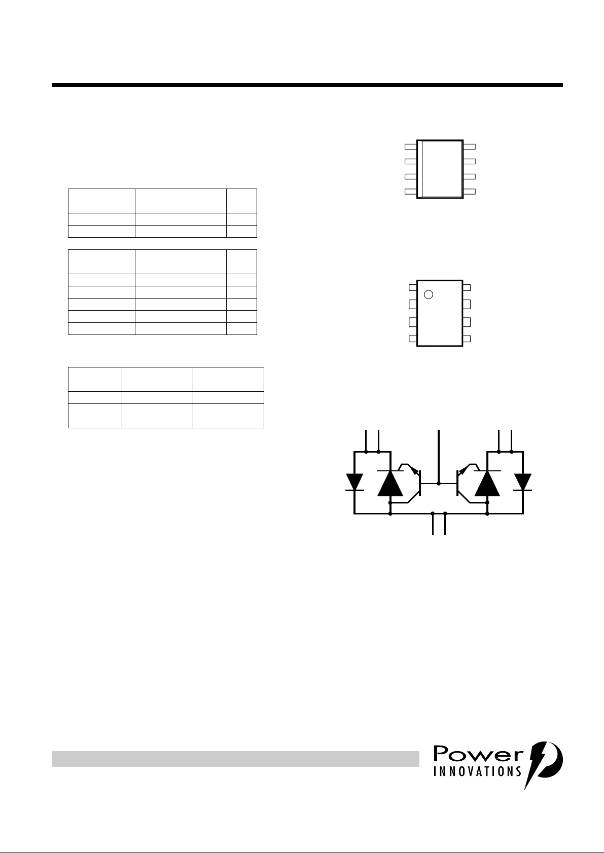
DUAL FORWARD-CONDUCTING P-GATE THYRISTORS
PROGRAMMABLE OVERVOLTAGE PROTECTORS
NOVEMBER 1995 - REVISED FEBRUARY 1998Copyright © 1998, Power Innovations Limited, UK
D PACKAGE
(TOP VIEW)
I
TSP
K1
Tip
G
Gate
NC
K2
Rin
A
Terminal t
NC - No internal connection
1
2
3
45
pical application names shown in
parenthesis
8
K1
Tip
7
6
A
A
K2
Ground
Ground
Rin
MD6XAN
60 Hz POWER
FAULT TIME
100 ms 4.5.13 Second-Level 2 11
1 s 4.5.13 Second-Level 2 4.5
5 s 4.5.13 Second-Level 2 2.4
300 s 4.5.13 Second-Level 1 0.95
900 s 4.5.13 Second-Level 1 0.93
●
2/10 Protection Voltage Specified
ELEMENT
Diode 6 8
Crowbar
= -48 V
V
GG
●
Also Rated for ITU-T 10/700 impulses
●
Surface Mount and Through-Hole Options
‘1089 TEST CLAUSE
AND TEST #
FIRST-LEVEL
V @ 56 A
-57 -60
I
TSM
A
SECOND-LEVEL
V @ 100 A
P PACKAGE
(TOP VIEW)
Tip
Gate
Rin
Terminal t
1
K1
2
G
3
NC
45
K2
NC - No internal connection
pical application names shown in
parenthesis
8
7
6
K1
A
A
K2
Tip
Ground
Ground
Rin
MD6XAV
- TISP61089P for Plastic DIP
- TISP61089D for Small-Outline
- TISP61089DR for Small-Outline Taped and
Reeled
description
The TISP61089 is a dual forward-conducting
buffered p-gate overvoltage protector. It is
designed to protect monolithic SLICs (Subscriber
Line Interface Circuits) against overvoltages on
the telephone line caused by lightning, a.c.
power contact and induction. Th e TISP61089 limits voltages that exceed the SLIC supp ly rail voltage. The
TISP61089 parameters are specified to allow equipment compliance with Bellcore GR-1089-CORE, Issue 1.
The SLIC line driver section is typically powered from 0 V (ground) and a negative voltage in the region of
-10 V to -75 V. The protector gate is connected to this negative supply. This references the protection
(clipping) voltage to the ne gative supply voltage. As the pro tectio n voltage wil l then track the nega tive supply
voltage the overvoltage stress on the SLIC is minimised.
Positive overvoltages are cl ipped to ground by diode forward condu ction. Negative overvoltages are i nitially
clipped close to the SLIC negative supply rail value. If sufficient current is available from the overvoltage, then
PRODUCT INFORMATION
Information is current as of publication date. Products conform to specifications in accordance
with the terms of Power Innovations standard warranty. Production processing does not
necessarily include testing of all parameters.
1
Page 2

TISP61089
DUAL FORWARD-CONDUCTING P-GATE THYRISTORS
PROGRAMMABLE OVERVOLTAGE PROTECTORS
NOVEMBER 1995 - REVISED FEBRUARY 1998
the protector will c rowbar int o a low voltage on-s tate cond ition. As the overvoltage subs ides the high holdi ng
current of the crowbar prevents d.c. latchup.
The TISP61089 is intended to be used with a series combination of a 25Ω or higher resistance and a suitable
overcurrent protector. Power fault compliance requires the series overcurrent element to open-circuit or
become high impedance (see Applications Information). For equipment compliant to ITU-T recommendations
K20 or K21 only, the series resistor value is set by the power cross requirements. For K20 and K21, a
minimum series resistor value of 10Ω is recommended.
These monolithic protection devices a re fabricated in ion-impla nted planar ver tical power structures for high
reliability and in normal system operation they are virtually transparent. The TISP61089 buffered gate design
reduces the loading on the SLIC supply during overvoltages caused by power cross and induction. The
TISP61089 is available in 8-pin plastic small-outline surface mount package and 8-pin plastic dual-in-line
package.
absolute maximum ratings
RAT ING SYMBOL VALUE UNIT
≤
Repetitive peak off-state voltage, I
Repetitive peak gate-cathode voltage, V
Non-repetitive peak on-state pulse current (see Notes 1 and 2)
10/1000 µs (Bellcore GR-1089-CORE, Issue 1, November 1994, Section 4)
5/320 µs (ITU-T recommendation K20 & K21, open-circuit voltage wave shape 10/700)
1.2/50 µs (Bellcore GR-1089-CORE, Issue 1, November 1994, Section 4, Alternative) 100
2/10 µs (Bellcore GR-1089-CORE, Issue 1, November 1994, Section 4) 120
Non-repetitive peak on-state current, 60 Hz (see Notes 1 and 2)
0.1 s 11
1s
5s
300 s
900 s
Non-repetitive peak gate current, 1/2 µs pulse, cathodes commoned (see Notes 1 and 2) I
Operating free-air temperature range T
Junction temperature T
Storage temperature range T
= 0, -40°C≤T
G
= 0, -40°C≤T
KA
85°C V
J
≤
85°C V
J
DRM
GKRM
I
TSP
I
TSM
GSM
A
J
stg
-100 V
-85 V
30
40
4.5
2.4
0.95
0.93
40 A
-40 to +85 °C
-40 to +150 °C
-40 to +150 °C
A
A
NOTES: 1. Initially the protector must be in thermal equilibrium with -40°C≤T
its initial conditions.
2. The rated current values may be applied either to the Ring to Ground or to the Tip to Ground ter minal pairs. Additionally, both
terminal pairs may have thei r rated current values applied simultaneously (in this case the Ground terminal current will be twice the
rated current value of an individual terminal pair). Above 85°C, derate linearly to zero at 150°C lead temperature.
recommended operating conditions
C
Gate decoupling capacitor 100 220 nF
G
TISP61089 series resistor for first-level and second-level surge survival
R
S
TISP61089 series resistor for first-level surge survival
PRODUCT INFORMATION
2
≤
85°C. The surge may be repeated after the device returns to
J
MIN TYP MAX UNIT
40
25
Ω
Page 3
DUAL FORWARD-CONDUCTING P-GATE THYRISTORS
PROGRAMMABLE OVERVOLTAGE PROTECTORS
electrical characterist ics, TJ = 25°C (unless otherwise noted)
PARAMETER TEST CONDITIONS MIN TYP MAX UNIT
I
D
V
V
V
I
H
I
GAS
I
GT
V
Q
C
(BO)
F
FRM
GT
GS
AK
Off-state current VD=-85V, VGK=0
Ω,
VGG=-48V, CG= 220 nF
Ω,
VGG=-48V, CG= 220 nF
Ω,
VGG=-48V, CG= 220 nF
Ω,
VGG=-48V, CG= 220 nF
Breakover voltage
2/10 µs, I
2/10 µs, I
1.2/50 µs, I
1.2/50 µs, I
= -56 A, RS=45
T
= -100 A, RS=50
T
=-53A, RS=47
T
=-96A, RS=52
T
Forward voltage IF= 5 A, tw= 200 µs 3V
Ω,
VGG=-48V, CG= 220 nF
Ω,
VGG=-48V, CG= 220 nF
Ω,
VGG=-48V, CG= 220 nF
Ω,
VGG=-48V, CG= 220 nF
Peak forward recov ery
voltage
2/10 µs, I
2/10 µs, I
1.2/50 µs, I
1.2/50 µs, I
=56A, RS=45
F
= 100 A, RS=50
F
=53A, RS=47
F
=96A, RS=52
F
Holding current IT= -1 A, di/dt = 1A/ms, VGG= -48 V -150 mA
Gate reverse current VGG=VGK=-75V, VKA=0
≥
Gate trigger current IT= 3 A, t
Gate trigger voltage IT= 3 A, t
p(g)
p(g)
20 µs, V
≥
20 µs, V
=-48V 5 mA
GG
=-48V 2.5 V
GG
Gate switching charge 1.2/50 µs, IT=53A, RS=47Ω, VGG= -48 V CG= 220 nF 0.1 µC
Anode-cathode off-
state capacitance
f=1MHz, V
=1V, IG= 0, (see Note 3)
d
T
T
T
T
V
V
TISP61089
NOVEMBER 1995 - REVISED FEBRUARY 1998
= 25°C -5 µA
J
= 85°C -50 µA
J
-57
-60
-60
-64
6
8
8
12
= 25°C -5 µA
J
= 85°C -50 µA
J
= -3 V 100 pF
D
=-48V 50 pF
D
V
V
NOTE 3: These capacitance mea surements employ a three terminal capacitance bridge incorporating a guard circuit. The unmeasured
device terminals are a.c. connected to the guard terminal of the bridge.
thermal characteristics
PARAMETER TEST CONDITIONS MIN TYP MAX UNIT
P
=0.8W, TA= 25°C
R
Junction to free air thermal resistance
θ
JA
tot
5cm
2
, FR4 PCB
D Package 160
P Package 100
°C/W
PRODUCT INFORMATION
3
Page 4
TISP61089
DUAL FORWARD-CONDUCTING P-GATE THYRISTORS
PROGRAMMABLE OVERVOLTAGE PROTECTORS
NOVEMBER 1995 - REVISED FEBRUARY 1998
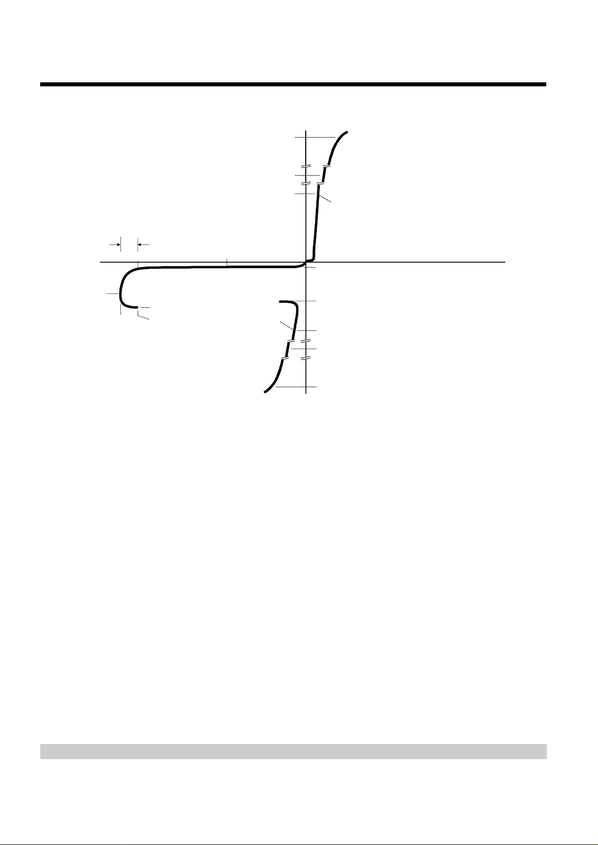
PARAMETER MEASUREMENT INFORMATION
-v
I
(BO)
V
Quadrant III
Switching
Characteristic
V
(BO)
GK(BO)
V
+i
I
(= |I
TSP
|)
FSP
Characteristic
I
(= |I
FSM
GG
I
S
V
S
V
D
|)
TSM
I
F
V
F
I
D
I
H
V
T
I
T
I
TSM
I
TSP
-i
Quadrant I
Forward
Conduction
+v
PM6XAAA
Figure 1. VOLTAGE-CURRENT CHARACTERISTIC
PRODUCT INFORMATION
4
Page 5
g
10
DUAL FORWARD-CONDUCTING P-GATE THYRISTORS
PROGRAMMABLE OVERVOLTAGE PROTECTORS
NOVEMBER 1995 - REVISED FEBRUARY 1998
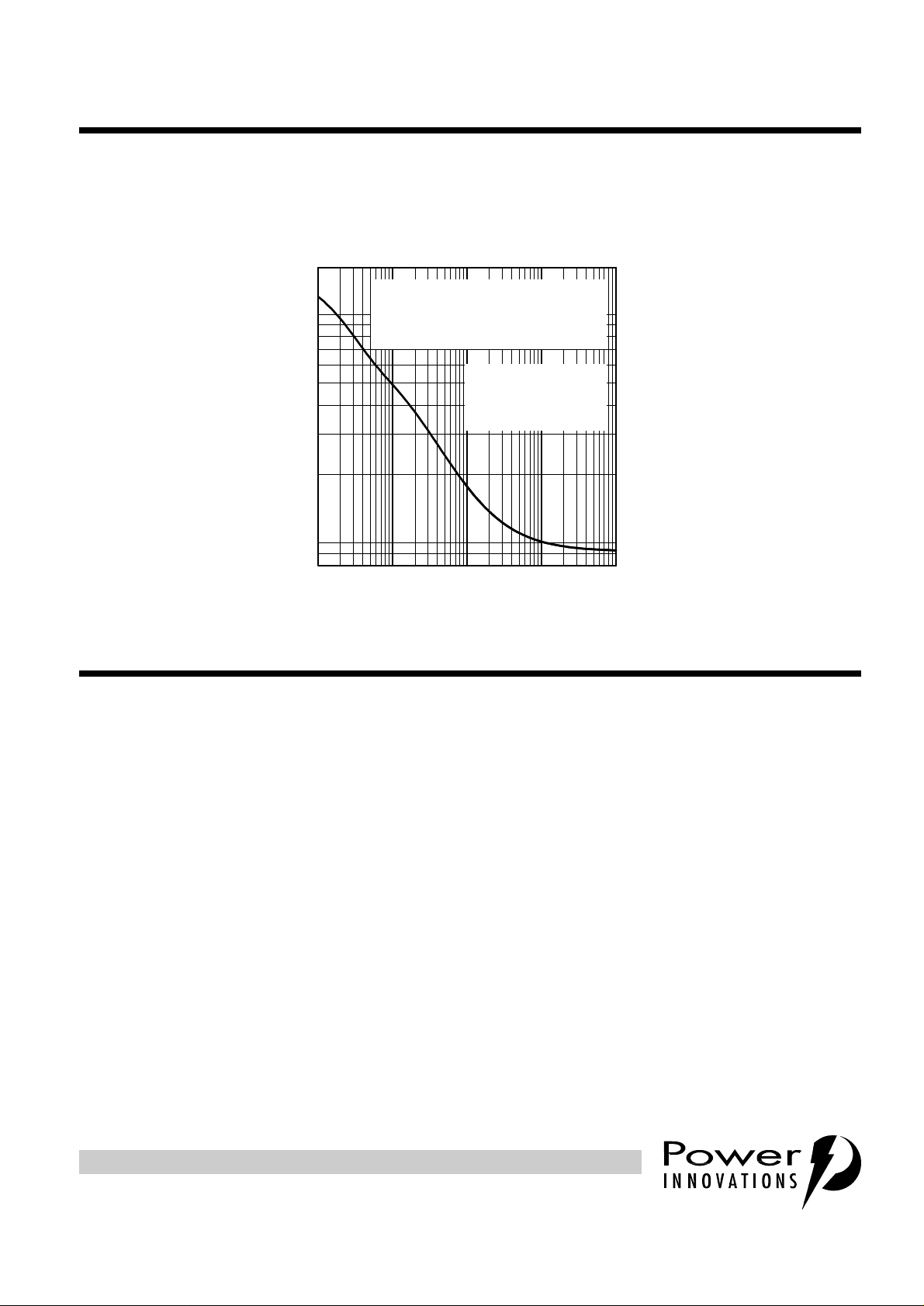
THERMAL INFORMATION
PEAK NON-RECURRING A.C.
vs
CURRENT DURATION
RING AND TIP CONNECTIONS -
applied simultaneously to both
I
TSM
GROUND CONNECTION Return current is twice I
V
GEN
R
GEN
VG = -48 V, T
TSM
= 600 Vrms
= 70 to 950
AMB
TI6LACA
Ω
= 85°C
TISP61089
- Peak Non-Recurrent 60 Hz Current - A
TSM
1
I
0·1 1 10 100 1000
t - Current Duration - s
Fi
ure 2. NON-REPETITIVE PEAK ON-STATE CURRENT AGAINST DURATION
APPLICATIONS INFORMATION
gated protectors
This section covers three topics. Firstly, it is explained why gated protectors are needed. Second, the voltage
limiting action of the protector is described. Third, an example application circuit is described.
purpose of gated protectors
Fixed voltage thyristor overvoltage protectors have been used si nce the early 1980s to protect mo nolithic
SLICs (Subscriber Line Interface Circuits) against overvoltages on the telephone line caused by lightning, a.c.
power contact and induction. As the SLIC was usuall y powered from a fixed voltage negative supply rail, the
limiting voltage of the protector could als o be a fixed value. The TISP1072F3 is a typical example of a fixed
voltage SLIC protector.
SLICs have become more sophisticated. T o minimise power consumption, some designs automatically adjust
the supply voltage, V
supply voltage would be set low, but for long lines, a higher supply voltage would be generated to drive
sufficient line curren t. The optimum protection for this type of SLIC would be given by a protection voltage
which tracks the SLIC supply voltage. This can be achieved by connecting the protection thyr istor ga te t o the
SLIC supply, Figure 3. This gated (programmable) protection arrangement minimises the voltage stress on
the SLIC, no matter what value of supply voltage.
, to a value that is just sufficient to drive the requir ed line cu rrent. For shor t line s the
BAT
PRODUCT INFORMATION
5
Page 6
TISP61089
g
)
DUAL FORWARD-CONDUCTING P-GATE THYRISTORS
PROGRAMMABLE OVERVOLTAGE PROTECTORS
NOVEMBER 1995 - REVISED FEBRUARY 1998
TIP
WIRE
Ω
600
GENERATOR
SOURCE
RESISTANCE
Ω
600
A.C.
GENERATOR
0 - 600 Vrms
Fi
ure 3. TISP61089 BUFFERED GATE PROTECTOR (SECTION 4.5.12 TESTING CONDITION
RING
WIRE
R1a
>25
R1b
>25
Ω
Ω
TISP61089
Th4
Th5
C1
220 nF
SLIC
SWITCHING MODE
POWER SUPPLY
Tx
I
I
SLIC
G
I
BAT
C2
V
BAT
D1
AI6XAG
operation of gated protectors
Figures 4. and 5. show how the TISP61089 limits neg ative and positive overvoltages. Positive overvoltages
(Figure 5) are clipped by the antiparallel diodes in th e TISP61089 and the resulting current is diver ted to
ground. Negative overvoltages (Figure 4.) are initially clipped clos e to the SLIC negative supply rail value
). If sufficient curren t is available from the overvoltage, then the protector (Th5) wil l crowbar into a low
(V
BAT
voltage on-state conditio n. As the overvoltage sub sides th e high holdin g current o f th e crowbar prevents d.c.
latchup. The protection voltage will be th e sum of t he gate su pply (V
(V
). The protection voltage will be i nc reas ed if th er e is a l ong c on necti on bet ween t he gat e d ec oup li ng
GK(BO)
capacitor, C1, and the gate terminal. During the in iti al rise of a fast impulse, the gat e c ur rent (I
as the cathode current (I
). Rates of 70 A/µs can cause inductive voltages of 0.7 V in 2.5 cm of printed wiring
K
) and the peak gate-c athode voltage
BAT
) is the same
G
track. To minimi se this inductive voltage increase of protection voltage, the length of the c apacitor to gate
terminal tracking should be minimised. Inductive voltages in the protector cathode wiring will also increase the
protection voltage. These voltages can be minimised by routing the SLIC connection through the protector as
shown in Figure 3.
PROTECTOR
CROWBAR
OPERATION
I
K
61089
Th5
TISP
C1
220 nF
SLIC
I
G
V
BAT
AI6XAH
PROTECTOR
DIODE
OPERATION
I
F
61089
Th5
TISP
C1
220 nF
SLIC
V
BAT
AI6XAI
Figure 4. NEGATIVE OVERVOLTAGE CONDITION Figure 5. POSITIVE OVERVOLTAGE CONDITION
PRODUCT INFORMATION
6
Page 7

TISP61089
g
DUAL FORWARD-CONDUCTING P-GATE THYRISTORS
PROGRAMMABLE OVERVOLTAGE PROTECTORS
NOVEMBER 1995 - REVISED FEBRUARY 1998
In Figure 6, the positive gate cha rge (QGS) is about 0.1 µC which, wit h the 0.1 µF ga te decoupl ing capa citor
used, increased the gate supply by about 1 V (= Q
volt age, V
. This increase does not directly add to the protection voltage as the supply voltage change
BAT
reaches a maximum at 0.4 µs whe n the gate current reverses polarity; wherea s the pr otection voltage peaks
at 0.3 µs. In Figure 6, the peak clamping voltage (V
supply voltage. This 5.5 V increase is the sum of the supply rail increase at that time, (0.5 V), and the
protection circuits catho de diode to su pply rail breakover voltage (5 V). In practice, use of the recomme nded
220 nF gate decoupling capacitor would give a supply rail increase of 0.25 V and a V
-77.25 V.
0
-20
/C1). This change is just visible on the -72 V gate
GS
) is -77.5 V, an increase o f 5. 5 V on t he nomin al gat e
(BO)
value of about
(BO)
V
-40
Voltage - V
-60
-80
0.0 0.5 1.0 1.5
1
Q
GS
0
-1
-2
Current - A
-3
-4
-5
0.0 0.5 1.0 1.5
K
Time - µs
I
G
Time - µs
V
BAT
I
K
Fi
ure 6. PROTECTOR FAST IMPULSE CLAMPING AND SWITCHING WAVEFORMS
application circuit
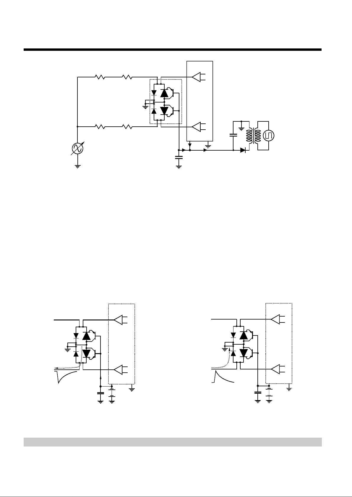
Figure 7 shows a typical TISP61089 SLIC card protection circuit. The incoming line conductors, Ring (R) and
Tip (T), connect to the rel ay matrix via t he ser ies overcurrent prot ect ion. Fusible resisto rs, fuses and posit ive
temperature coefficient (PTC) resistors can be used for overcurrent protection. Resistors will reduce the
prospective current from the surge generator for both the TISP61089 and the ring/test protector. The
TISP7xxxF3 protector has the same prote ction voltage for any ter minal pair. This protector is us ed when the
ring generator configuration may be ground or battery-backed. For dedicated ground-backed ringing
generators, the TISP3xxxF3 gives better protection as its inter-conductor protection voltage is twice the
conductor to ground value.
PRODUCT INFORMATION
7
Page 8

TISP61089
g
DUAL FORWARD-CONDUCTING P-GATE THYRISTORS
PROGRAMMABLE OVERVOLTAGE PROTECTORS
NOVEMBER 1995 - REVISED FEBRUARY 1998
TIP
WIRE
RING
WIRE
OVER-
CURRENT
PROTECTION
R1a
R1b
RING/TEST
PROTECTION
Th1
Th3
Th2
TISP
3xxxF3
OR
7xxxF3
Fi
TEST
RELAY
S1a
S1b
TEST
EQUIP-
MENT
RING
RELAY
S2a
S2b
RING
GENERATOR
SLIC
RELAY
S3a
S3b
ure 7. TYPICAL APPLICATION CIRCUIT
SLIC
PROTECTOR
Th4
Th5
TISP
61089
C1
220 nF
SLIC
V
BAT
AI6XAJ
Relay contacts 3a and 3b connect the line conductors to the SLIC via the TISP61089 protector. The protector
gate reference voltage comes from the SLIC neg ative supply (V
). A 220 nF gate capacitor sources the
BAT
high gate current pulses caused by fast rising impulses.
LSSGR 1089
GR-1089-CORE, “1089”, covers electromagnetic compatibility and electrical safety generic criteria for US
network teleco mmunica tion eq uipmen t. It is a mod ule in Volume 3 of LSSGR (LATA (Local Access Transport
Area) Switching Syste ms Ge ner ic Requ ireme nts, FR-NWT-000064). In 1089 surge a nd power fault immunity
tests are done at two levels. After first-level testing the equipment shall not be damaged and shall continue to
operate correctly. Under second level testing the equipment shall not become a safety hazard. The equipment
is permitted to fail as a result of second-level testing. When the equipment is to be located on customer
premises, second-level testing incl udes a wiring simula tor test, which requ ires the equipment to reduce the
power fault current below certain values.
The following clauses reference the 1089 section and ca lc ulate th e pr otec tor s tre ss levels. The TISP61089 is
specified for use with a 40Ω series resistor. This resistor value will ensure that the TISP61089 survives
second level surge testing. Values down to 25Ω may be used if some second level surge failure is
acceptable. All the tabulated values are for a series re si st ance of 40Ω. Peak current values for a 25Ω series
resistor are covered in the clause te xt.
The values of protector c urrent are cal culated from the open circui t generator voltage di vided by the sum of
the total circuit resistance. The total circuit resistance is the sum of the generator fictive source resistance and
the TISP61089 ser ies resi stor value. Most generators have multiple outputs and e ach ou tput connects to an
individual line conductor. For those generators that have a single output, each conductor will have an effective
generator fictive source resistance of n times the generator fictive source resistance, where n is the number of
conductors simultaneously tested.
PRODUCT INFORMATION
8
Page 9

TISP61089
DUAL FORWARD-CONDUCTING P-GATE THYRISTORS
PROGRAMMABLE OVERVOLTAGE PROTECTORS
NOVEMBER 1995 - REVISED FEBRUARY 1998
section 4.5.7 - first-level surge testing
The two most significant test wave shapes in this section are the high energy 10/1000 and the high current
2/10. As shown in table 1, the peak currents for these surges are 2x20 A and 2x56 A respectively. The
protector must survive the 2x20 A 10/1000 surge and the TISP61089 will do this as its rating is 2x30 A. When
both conductors are surg ed simultaneo usly the retur n ( anode) cu rrent wil l be 40 A, agai n the TISP61 089 will
survive this as its rating for this condition will be 60 A. Similarly the TISP61089 will survive the 2x56 A 2/10 as
its rating is 2x120 A.
table 1. first-level surge currents
GENERATOR
WAVE SHAPE
2/10 2500 500 5 45 2x56
OPEN-CIRCUIT
VOLTAGE
V
SHORT-CIRCUIT
CURRENT
A
FICTIVE
SOURCE
RESISTANCE
Ω
TOTAL CIRCUIT
RESISTANCE
Ω
I
T
A
1.2/50, 8/20
(See Text)
10/360 1000 100 10 50 2x20
10/1000 600 100 6 46 2x13
10/1000 1000 100 10 50 2x20
The highest protection voltage will be for the 56 A 2/10 wave shape. Under this c onditi on the average rate of
current rise will be 56/2 = 28 A/µs. The value of diode and thyristor voltage under this condition is specified in
the electrical characteristics.
Compared to TR-NWT-001089, Issue 1, October 19 91, GR -1089-CORE , Issue 1, November 19 94, adds the
alternative of using the IEEE C62.41 1.2/50-8/20 combination wave generator for the 2/10 test. This generator
usually has a single outp ut and a fictive resist ance of 2Ω. The 2/10 generator has a fictive output res ista nce
5Ω, (2500/500), and GR-1089-CORE compensates for this by adding an extra 3Ω in the output of the 1.2/508/20 generator. In practice, the extra 3Ω causes the prospective short-circuit current wave shape to be similar
to the 1.2/50 open-cir cuit voltage wave shape. The TISP61089 will surv ive the 2x53 A 1.2/50 a s its rating is
2x100 A.
Using a 25Ω series resistor will result in table 1. I
TISP61089 will survive these peak current values as they are lower than the TISP61089 ratings.
section 4.5.8 - second-level surge testing
This is a 2/10 wave shape test. As shown in table 2, the peak current for this surge is 2x100 A. The
TISP61089 will survive the 2x100 A 2/10 surge as its rating is 2x120 A.
2500 360 4 + 3 47 2x53
column values of 2x83, 2x78, 2x29, 2x19 and 2x29. The
T
Under this condition t he average rate of current r ise will be 100/2 = 5 0 A/µs. The value of dio de and thyris tor
voltage under this condition is specified in the electrical characteristics.
Compared to TR-NWT-001089, Issue 1, October 19 91, GR -1089-CORE , Issue 1 , November 1994, adds th e
alternative of using the IEEE C62.41 1.2/50-8/20 combination wave generator for the 2/10 test. The 2/10
generator has a fictive output resistance 10Ω, (5000/500), and GR-1089-CORE compensates for this by
adding an extra 8Ω in the output of the 1.2/50-8/20 generator. In practice, the extra 8Ω causes the
PRODUCT INFORMATION
9
Page 10

TISP61089
DUAL FORWARD-CONDUCTING P-GATE THYRISTORS
PROGRAMMABLE OVERVOLTAGE PROTECTORS
NOVEMBER 1995 - REVISED FEBRUARY 1998
table 2. second-level surge current
WAVE SHAPE
2/10 5000 500 10 50 2x100
1.2/50, 8/20
(See Text)
prospective shor t-ci rcuit cu rrent wave shape to be similar to the 1.2/50 open-c ircuit voltage wave shape. The
TISP61089 will survive the 2x96 A 1.2/50 as its rating is 2x100 A.
Using a 25Ω series resisto r wil l resu lt in table 2. I
fail at these peak current values as they are higher than the TISP61089 ratings.
section 4.5.9 - Intra-building surge testing
These tests use a 2/10 wave shape. As shown in table 3, the peak currents for this test are 2x27 A and 17 A.
The TISP61089 can survive both these levels as its rating is 2x120 A.
OPEN-CIRCUIT
VOLTAGE
V
5000 420 4 + 8/conductor 52 2x96
SHORT-CIRCUIT
CURRENT
A
column values of 2x14 3 an d 2 x1 35. The TI SP 610 89 m ay
T
GENERATOR
FICTIVE
SOURCE
RESISTANCE
Ω
TOTAL
CIRCUIT
RESISTANCE
Ω
table 3. intra-building surge currents
GENERATOR
WAVE SHAPE
OPEN-CIRCUIT
VOLTAGE
V
SHORT-CIRCUIT
CURRENT
A
FICTIVE
SOURCE
RESISTANCE
Ω
TOTAL CIRCUIT
RESISTANCE
Ω
I
T
A
I
T
A
2/10 1500 100 15 55 2x27
800 100 8 48 17
1.2/50, 8/20
(See Text)
Compared to TR-NWT-001089, Issue 1, October 1991, GR-108 9-CORE, Issue 1, November 1994, the 2/10
alternative of using a CCITT Recommendation K.22 1.2/50-8/20 combination wave generator has been
changed to an IEEE C6 2.41 1.2/50-8/20 gene rator. This generator usually has a single o utput and a fictive
resistance of 2Ω. The 2/10 generator has fictive output resistances of 15Ω and 8Ω. GR-1089-CORE
compensates for this by adding an extra resistances of 12Ω and 6Ω in the output of the 1.2/50-8/20
generator. In practice, this extra resistance causes the p rospective short-circuit current wave shape to be
similar to the 1.2 /50 open-circuit voltage wave shape. The TISP 61089 will sur vive the 2x27 A 1.2/50 as its
rating is 2x100 A.
Using a 25Ω series resistor wil l res ul t in ta ble 3. I
will survive these peak current values as they are lower than the TISP61089 ratings.
1500 94 4 + 12/conduc-
tor
800 100 2 + 6 48 17
column values of 2x38, 24, 2x37 and 24. The TI SP61089
T
56 2x27
PRODUCT INFORMATION
10
Page 11

TISP61089
DUAL FORWARD-CONDUCTING P-GATE THYRISTORS
PROGRAMMABLE OVERVOLTAGE PROTECTORS
NOVEMBER 1995 - REVISED FEBRUARY 1998
section 4.5.12 - first-level power fault testing
The most significant tests are a long duration (900 s) medium current test and a higher current tests of 60 one
second power applications. As sh own in table 4, the peak curren ts for these tests are 2x0.37 A and 2x1.3 A
respectively. The TISP61089 will sur vive both these conditions as its rat ings are 2x0.93 A and 2x4.5 A for
these time periods
table 4. first-level power fault currents
A.C.
DURATION
s
1 200 0.33 600 640 2x0.31 2x0.44
1 400 0.67 600 640 2x0.63 2x0.88
1 600 1 600 640 2x0.94 2x1.3
1 1000 1 1000 1040 2x0.96 2x1.3
900 50 0.33 150 190 2x0.26 2x0.37
900 100 0.17 590 630 2x0.16 2x0.22
Using a 25Ω series resistor will result in table 4. I
2x0.23. The TISP61089 will survive these peak current values as they are lower than the TISP61089 ratings.
section 4.5.13 - second-level power fault testing
The two most significant test s are a long duratio n (900 s) mediu m current test and a hi gher current 5 s tes t.
As shown in table 5, the peak currents for these tests are 2x17 A and 2x7.7 A respectively. For the
TISP61089 to survive this test, the series current limiting element must operate within 0.1 s and 0.5 s
respectively.
OPEN-CIRCUIT
RMS VOLTAGE
V
SHORT-CIRCUIT
RMS CURRENT
A
SOURCE
RESISTANCE
Ω
column values of 2x0.45, 2x0.9, 2x1.4, 2x1.4, 2x0.4 and
TM
TOTAL CIRCUIT
RESISTANCE
Ω
I
TRMS
A
table 5. second-level po wer fault currents
I
TM
A
A.C.
DURATION
s
5 600 60 10 50 2x12 2x17
5 600 7 86 126 2x4.8 2x6.8
900 120 25 5 45 2x2.7 2x3.8
900 277 25 11 51 2x5.4 2x7.7
900 100 0.37 273 313 2x0.32 2x0.45
900 300 1.1 273 313 2x0.96 2x1.4
900 600 2.2 273 313 2x1.9 2x2.7
Using a 25Ω series resistor will result in table 5. I
and 2x2.9. The TISP61089 wi ll probably fail for a peak curren t level of 2x24 A and the ser ies curre nt limitin g
OPEN-CIRCUIT
RMS VOLTAGE
V
SHORT-CIRCUIT
CURRENT
A
SOURCE
RESISTANCE
Ω
column values of 2x24, 2x7.7, 2x5.7, 2x11, 2x0.47, 2x1.4
TM
TOTAL
CIRCUIT
RESISTANCE
Ω
I
TRMS
A
PRODUCT INFORMATION
I
TM
A
11
Page 12

TISP61089
DUAL FORWARD-CONDUCTING P-GATE THYRISTORS
PROGRAMMABLE OVERVOLTAGE PROTECTORS
NOVEMBER 1995 - REVISED FEBRUARY 1998
element must operate i n under 0.1 s to prevent exceeding the TISP610 89 package limit. For 2x7.7 A, the
series current limiting element must operate within 0.4 s for TISP61089 survival.
section 4.5.15 - second-level power fault testing with wiring simulator
The purpose o f this test is to ens ure that the telephone c able does not become a hazard due to excessive
current. A seri es fuse, type MDQ 1- 6/10A, simula tes the sa fe current levels of a telephone cable. If this fus e
opens the equipment fails the test. For the equipment to pass, the equipment series overcurrent element must
reduce the current to below the MDQ 1-6/10A fusing level to prevent the simulator operating. The a.c. test
voltage can range from zero to 600 V, which gives a maximum co nductor cur rent of 10 A. Table 6 shows the
simulator fusing times for three current levels.
table 6. second-level power fault currents with MDQ 1-6/10A fuse
A.C.
DURATION
s
1000 100 5 20 60 1.7 2.4
1000 300 15 20 60 5.0 7.1 30
1000 600 30 20 60 10 14 0.7
Using a 25Ω series resistor will result in table 6. I
operating times will be ∞, 12 s and 0.4 s respectively
For the equipment to pass this test, the TIS P61089 series cu rrent limiting element must ope rate before the
MDQ 1-6/10A fusing times shown in table 7.
OPEN-CIRCUIT
RMS VOLTAGE
V
SHORT-
CIRCUIT
CURRENT
A
SOURCE
RESISTANCE
Ω
column values of 2x3.1, 2x9.4 and 2x19. Simulator
TM
TOTAL
CIRCUIT
RESISTANCE
Ω
I
TRMS
A
I
TM
A
table 7. operating times of MDQ 1-6/10A fuse
TIME TO
OPERATE
s
0.2 17
0.5 12
I
RMS
A
TIME
TO
OPEN
s
∞
19
57
10 6.8
1000 2.5
overcurrent protection
To meet ‘1089, the overcurrent protection must be coordinated with the requirements of sections 4.5.7, 4.5.8,
4.5.9, 4.5.12, 4.5.13, 4.5.15 and the TISP61089. The overcurrent protection must not fail in the first level tests
of sections 4.5.7, 4.5.9 and 4.5.12. Recoverable overcurrent protectors (e.g. Positive Temperature Coefficient
Resistors) may operate during first level testing, but normal equipment working must be restored after the test
has ended. The test current levels and their duration are shown in Figure 8. First level tests have a high
source resistance and the current levels are not strongly dependent on the TISP61089 series resistor value.
PRODUCT INFORMATION
12
Page 13

TISP61089
g
DUAL FORWARD-CONDUCTING P-GATE THYRISTORS
PROGRAMMABLE OVERVOLTAGE PROTECTORS
NOVEMBER 1995 - REVISED FEBRUARY 1998
Second level tests have a low source resistance and the curre nt levels are dependent on the TISP61089
series resisto r value. The two stepped lines at the top of Fig ure 8 are for the 25Ω and 40Ω series resistor
cases. If the full current-time duration s occur the equipment will fail the wiri ng simulator test. The MDQ 1-6/
10A fusing characteristic is also shown in Figure 8. The TISP61089 series overcurrent protection must
operate before the MDQ 1-6/10A fuses, so this represents ano ther bou ndar y c ondition in the selection of the
overcurrent protector.
MAXIMUM RMS CURRENT
vs
AI6XAK
Ω
Ω
Ω
Maximum RMS Current - A
30
20
10
0.7
0.5
0.3
0.2
TIME
Second Level Tests - 25
7
5
3
2
1
Second Level Tests - 40
MDQ 1-6/10A Fuse
First Level Tests - 25 & 40
0.1
0.01 0.1 1 10 100 1000
Fi
ure 8. ‘1089 MAXIMUM TEST CURRENT LEVEL
Time - s
Figure 9 summarises these boundary conditions. The highest curren t levels that can flow are influenced by
the TISP61089 ser ies res is tan ce. Af ter on e sec ond the max i mum c urre nt-ti me b oun dary becomes s et by the
MDQ 1-6/10A fusing characteristic. Fusible overcurrent protectors cannot operate at first level current levels.
Figure 9 shows two other cur ves. The lower one is the TISP61089 rated curren t. The overcurrent protector
should not allow cur rent-time durations greater t han this otherwise the TISP61089 may fail. If second level
failure is acceptable then the overcurrent protector
must
operate before the TISP61089 package limit is
reached.
The TISP61089 a.c. ratings are worse ca se values when the device is mounted on the minimal sized PCB
used for measuring ther mal resistance. Typic al PCBs would give a 25% increase in the rated currents for
periods above 0.1 s.
PRODUCT INFORMATION
13
Page 14

TISP61089
DUAL FORWARD-CONDUCTING P-GATE THYRISTORS
PROGRAMMABLE OVERVOLTAGE PROTECTORS
NOVEMBER 1995 - REVISED FEBRUARY 1998
OVERCURRENT PROTECTOR OPERATION LIMITS
vs
TIME
Maximum RMS Current - A
30
Second Level Tests - 25
20
10
7
5
3
2
1
0.7
0.5
0.3
0.2
Second Level Tests - 40
Ω
Ω
AI6XAL
MDQ 1-6/10A Fuse
TISP61089 Package Limit
TISP61089 Survival
First Level Tests - 25 & 40
Ω
0.1
0.01 0.1 1 10 100 1000
Time - s
Figure 9. OVERCURRENT PROTECTOR REQUIREMENTS
PRODUCT INFORMATION
14
Page 15

TISP61089
p
DUAL FORWARD-CONDUCTING P-GATE THYRISTORS
PROGRAMMABLE OVERVOLTAGE PROTECTORS
NOVEMBER 1995 - REVISED FEBRUARY 1998
MECHANICAL DATA
D008
lastic small-outline package
This small-outline package c onsists of a circuit mounted on a lead frame and encapsulated with in a plastic
compound. The compound will withstand soldering temperature with no deformation, and circuit performance
characteristics will remain stable when operated in high humidity conditions. Leads require no additional
cleaning or processing when used in soldered assembly.
D008
6,20 (0.244)
5,80 (0.228)
1,75 (0.069)
1,35 (0.053)
4,00 (0.157)
3,81 (0.150)
8
1
7° NOM
3 Places
5,00 (0.197)
4,80 (0.189)
765
432
0,50 (0.020)
0,25 (0.010)
x 45°NOM
Designation per JEDEC Std 30:
PDSO-G8
5,21 (0.205)
4,60 (0.181)
0,203 (0.008)
0,102 (0.004)
0,79 (0.031)
0,28 (0.011)
ALL LINEAR DIMENSIONS ARE IN MILLIMETERS AND PARENTHETICALLY IN INCHES
NOTES: A. Leads are within 0,25 (0.010) radius of true position at maximum material condition.
B. Body dimensions do not include mold flash or protrusion.
C. Mold flash or protrusion shall not exceed 0,15 (0.006).
D. Lead tips to be planar within ±0,051 (0.002).
Pin Spacing
1,27 (0.050)
(see Note A)
6 Places
0,51 (0.020)
0,36 (0.014)
8 Places
0,229 (0.0090)
0,190 (0.0075)
7° NOM
4 Places
1,12 (0.044)
0,51 (0.020)
4° ± 4°
MDXXAA
PRODUCT INFORMATION
15
Page 16

TISP61089
p
DUAL FORWARD-CONDUCTING P-GATE THYRISTORS
PROGRAMMABLE OVERVOLTAGE PROTECTORS
NOVEMBER 1995 - REVISED FEBRUARY 1998
MECHANICAL DATA
P008
lastic dual-in-line package
This dual-in-line package co nsists of a circuit mounted on a lead frame and en capsulated within a plastic
compound. The compound will withstand soldering temperature with no deformation, and circuit performance
characteristics will remain stable when operated in high humidity conditions The package is intended for
insertion in mounting-hole rows on 7,62 (0.300) centres. Once the leads are compressed and inserted,
sufficient tension is provided to secure the package in the board during soldering. Leads require no additional
cleaning or processing when used in soldered assembly.
P008
Index
Dot
10,2 (0.400) MAX
8
1 2 3 4
7 6 5
1,78 (0.070) MAX
4 Places
Designation per JEDEC Std 30:
C
L
PDIP-T8
7,87 (0.310)
7,37 (0.290)
T.P.
6,60 (0.260)
6,10 (0.240)
C
L
5,08 (0.200)
MAX
Seating
Plane
0,51 (0.020)
MIN
3,17 (0.125)
2,54 (0.100) T.P.
6 Places
(see Note A)
ALL LINEAR DIMENSIONS ARE IN MILLIMETERS AND PARENTHETICALLY IN INCHES
NOTE A: Each pin centerline is located within 0,25 (0.010) of its true longitudinal position
0,533 (0.021)
0,381 (0.015)
8 Places
MIN
PRODUCT INFORMATION
16
105°
90°
8 Places
0,36 (0.014)
0,20 (0.008)
8 Places
MDXXABA
Page 17

TISP61089
DUAL FORWARD-CONDUCTING P-GATE THYRISTORS
PROGRAMMABLE OVERVOLTAGE PROTECTORS
NOVEMBER 1995 - REVISED FEBRUARY 1998
IMPORTANT NOTICE
Power Innovations Limited (PI) reserves the right to make changes to its products or to discontinue any semiconductor product
or service without notice, and advises its customers to verify, before placing orders, that the information being relied on is
current.
PI warrants performance of its semiconductor products to the specifications applicable at the time of sale in accordance with
PI's standard w ar r a nty. Testing and other quality co ntro l t echniques are utilized to the extent PI deems n ece ss ary to s upp ort t his
warranty. Specific testing of all parameters of each device is not necessarily performed, except those mandated by government
requirements.
PI assumes no liability for applications assistance, customer product design, software performance, or infringement of patents
or services described herein. Nor is any license, either express or implied, granted under any patent right, copyright, design
right, or other intellectual property right of PI covering or relating to any combination, machine, or process in which such
semiconductor products or services might be or are used.
PI SEMICONDUCTOR PRODUCTS ARE NOT DESIGNED, INTENDED, AUTHORISED, OR WARRANTED TO BE SUITABLE
FOR USE IN LIFE-SUPPORT APPLICATIONS, DEVICES OR SYSTEMS.
Copyright © 1998, Power Innovations Limited
PRODUCT INFORMATION
17
 Loading...