

Page 1
PROGRAMMABLE SLIC OVER VOLTAGE PROTECTION FOR LSSGR ‘1089
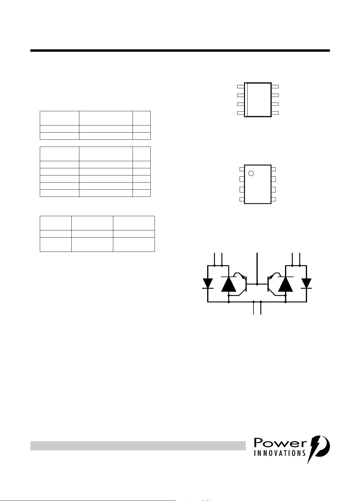
device symbol
Terminals K1, K2 and A correspond to the alternative
line designators of T, R and G or A, B and C. The
negative protection voltage is controlled by the voltage,
V
GG,
applied to the G terminal.
SD6XAE
A
K1 G K2
●
Dual Voltage-Programmable Protectors
- Wide 0 to -110 V Programming Range
- Low 5 mA max. Gate Triggering Current
- High 150 mA min. Holding Current
●
Rated for LSSGR ‘1089 Conditions
WAVE SHAPE
2/10 µs 4.5.8 Second-Level 1 120
10/1000 µs 4.5.7 First-Level 3 30
‘1089 TEST CLAUSE
AND TEST #
TISP61089A
DUAL FORWARD-CONDUCTING P-GATE THYRISTORS
PROGRAMMABLE OVERVOLTAGE PROTECTORS
D PACKAGE
(TOP VIEW)
I
TSP
(Tip)
(Gate)
K1
G
NC
K2
(Ring)
A
NC - No internal connection
Terminal typical application names shown in
1
2
3
45
parenthesis
8
K1
(Tip)
7
A
(Ground)
6
A
(Ground)
K2
(Ring)
JUNE 1999Copyright © 1999, Power Innovations Limited, UK
MD6XAN
60 Hz POWER
FAULT TIME
100 ms 4.5.13 Second-Level 2 10
1 s 4.5.13 Second-Level 2 4.4
5 s 4.5.13 Second-Level 2 2.1
300 s 4.5.13 Second-Level 1 0.84
900 s 4.5.13 Second-Level 1 0.83
●
2/10 Protection Voltage Specified
ELEMENT
Diode 6 8
Crowbar
= -48 V
V
GG
●
Also Rated for ITU-T 10/700 impulses
●
Surface Mount and Through-Hole Options
‘1089 TEST CLAUSE
AND TEST #
FIRST-LEVEL
V @ 56 A
-57 -60
I
TSM
A
SECOND-LEVEL
V @ 100 A
P PACKAGE
(TOP VIEW)
(Tip)
(Gate)
(Ring)
Terminal typical application names shown in
1
K1
2
G
3
NC
45
K2
NC - No internal connection
parenthesis
8
7
6
K1
A
A
K2
(Tip)
(Ground)
(Ground)
(Ring)
MD6XAV
- TISP61089AP for Plastic DIP
- TISP61089AD for Small-Outline
- TISP61089ADR for Small-Outline Taped
and Reeled
description
The TISP61089A is a dual forward-conducting
buffered p-gate overvoltage protector. It is
designed to protect monolithic SLICs (Subscriber
Line Interface Circuits) against overvoltages on
the telephone line caused by lightning, a.c.
power contact and induction. The TISP61089A lim its voltages that exceed the SLIC supply rail voltage. The
TISP61089A parameters are specified to allow equipment compliance with Bellcore GR-1089-CORE,
Issue 1.
The SLIC line driver section is typically powered from 0 V (ground) and a negative voltage in the region of
-10 V to -100 V. The protector gate is connected to this negative supply. This references the protection
(clipping) voltage to the negat ive supply voltage. As the p rotecti on voltage will th en track the negati ve supply
voltage the overvoltage stress on the SLIC is minimised.
PRODUCT INFORMATION
Information is current as of publication date. Products conform to specifications in accordance
with the terms of Power Innovations standard warranty. Production processing does not
necessarily include testing of all parameters.
1
Page 2

TISP61089A
DUAL FORWARD-CONDUCTING P-GATE THYRISTORS
PROGRAMMABLE OVERVOLTAGE PROTECTORS
JUNE 1999
Positive over voltages are clipp ed to ground by diode forward conduction. Ne gative overvoltages are initially
clipped close to the SLIC negative supply rail value. If sufficient current is available from the overvoltage, then
the protector will c rowbar in to a l ow voltage on-state cond ition. As the overvoltage sub side s the hi gh hol ding
current of the crowbar prevents d.c. latchup.
The TISP61089A is intended to be used with a ser ies combination of a 25Ω or higher resistance and a
suitable overcurrent protector. Power fault compliance requires the serie s overcurrent element to open- cir cuit
or become high impedance (see Applications Information). For equipment compliant to ITU-T
recommendations K20 or K21 only, the series resistor value is set by the power cross requirements. For K20
and K21, a minimum series resistor value of 10Ω is recommended.
These monolithic prote ction devices are fabricated in ion-implanted planar vertic al power structures for high
reliability and in normal system operation they are virtually transparent. The TISP61089A buffered gate
design reduces the loading on the SLIC supply dur ing overvoltages caused by power cross and induction.
The TISP61089A is available in 8-pin plas tic small-outlin e surface mount package and 8-pi n plastic dual-in line package.
absolute maximum ratings
RATING SYMBOL VALUE UNIT
≤
Repetitive peak off-state voltage, I
Repetitive peak gate-cathode voltage, V
Non-repetitive peak on-state pulse current (see Notes 1 and 2)
10/1000 µs (Bellcore GR-1089-CORE, Issue 1, November 1994, Section 4)
5/320 µs (ITU-T recommendation K20 & K21, open-circuit voltage wave shape 10/700)
1.2/50 µs (Bellcore GR-1089-CORE, Issue 1, November 1994, Section 4, Alternative) 100
2/10 µs (Bellcore GR-1089-CORE, Issue 1, November 1994, Section 4) 120
Non-repetitive peak on-state current, 60 Hz (see Notes 1 and 2)
0.1 s 10
1s
5s
300 s
900 s
Non-repetitive peak gate current, 1/2 µs pulse, cathodes commoned (see Notes 1 and 2) I
Operating free-air temperature range T
Junction temperature T
Storage temperature range T
= 0, -40°C≤T
G
= 0, -40°C≤T
KA
85°C V
J
≤
85°C V
J
DRM
GKRM
I
TSP
I
TSM
GSM
A
J
stg
-120 V
-120 V
30
40
4.4
2.1
0.84
0.83
40 A
-40 to +85 °C
-40 to +150 °C
-40 to +150 °C
A
A
NOTES: 1. Initially the protector must be in thermal equilibrium with -40°C≤T
its initial conditions.
2. The rated current values may be applied either to the Ring to Ground or to the Tip to Ground ter minal pairs. Additionally, both
terminal pairs may have their rated current values applied simultaneously (in this case the Ground terminal current will be twice the
rated current value of an individual terminal pair). Above 85°C, derate linearly to zero at 150°C lead temperature.
recommended operating conditions
C
Gate decoupling capacitor 100 220 nF
G
TISP61089A series resistor for first-level and second-level surge survival
R
S
TISP61089A series resistor for first-level surge survival
PRODUCT INFORMATION
2
≤
85°C. The surge may be repeated after the device returns to
J
MIN TYP MAX UNIT
40
25
Ω
Page 3
DUAL FORWARD-CONDUCTING P-GATE THYRISTORS
PROGRAMMABLE OVERVOLTAGE PROTECTORS
electrical characterist ics, TJ = 25°C (unless otherwise noted)
PARAMETER TEST CONDITIONS MIN TYP MAX UNIT
I
D
V
V
V
I
H
I
GKS
I
GT
V
Q
C
(BO)
F
FRM
GT
GS
AK
Off-state current VD=V
2/10 µs, I
Breakover voltage
2/10 µs, I
1.2/50 µs, I
1.2/50 µs, I
, IG=0
DRM
=-56A, RS=45
T
= -100 A, RS=50
T
= -53 A, RS=47
T
= -96 A, RS=52
T
Ω,
VGG=-48V, CG= 220 nF
Ω,
VGG=-48V, CG= 220 nF
Ω,
VGG=-48V, CG= 220 nF
Ω,
VGG=-48V, CG= 220 nF
Forward voltage IF= 5 A, tw= 200 µs 3V
Ω,
VGG=-48V, CG= 220 nF
Ω,
VGG=-48V, CG= 220 nF
Ω,
VGG=-48V, CG= 220 nF
Ω,
VGG=-48V, CG= 220 nF
Peak forward recovery
voltage
2/10 µs, I
2/10 µs, I
1.2/50 µs, I
1.2/50 µs, I
=56A, RS=45
F
= 100 A, RS=50
F
=53A, RS=47
F
=96A, RS=52
F
Holding current IT= -1 A, di/dt = 1A/ms, VGG= -48 V -150 mA
Gate reverse current VGG=VGK=V
Gate trigger current IT= 3 A, t
Gate trigger voltage IT= 3 A, t
p(g)
p(g)
GKRM
≥
20 µs, V
≥
20 µs, V
, VKA=0
=-48V 5 mA
GG
=-48V 2.5 V
GG
Gate switching charge 1.2/50 µs, IT=53A, RS=47Ω, VGG= -48 V CG= 220 nF 0.1 µC
Anode-cathode off-
state capacitance
f=1MHz, V
=1V, IG= 0, (see Note 3)
d
T
T
T
T
V
V
TISP61089A
JUNE 1999
= 25°C -5 µA
J
= 85°C -50 µA
J
-57
-60
-60
-64
6
8
8
12
= 25°C -5 µA
J
= 85°C -50 µA
J
= -3 V 100 pF
D
=-48V 50 pF
D
V
V
NOTE 3: These capacitance measurements employ a three terminal capacitance bridge incorporating a guard circuit. The unmeasured
device terminals are a.c. connected to the guard terminal of the bridge.
thermal characteristics
PARAMETER TEST CONDITIONS MIN TYP MAX UNIT
T
= 25 °C, EIA/JESD51-3
A
R
Junction to free air thermal resistance
θ
JA
PCB, EIA/JESD51-2
environment, P
TOT
= 1.7 W
D Package 120
°C/W
P Package 100
PRODUCT INFORMATION
3
Page 4
TISP61089A
DUAL FORWARD-CONDUCTING P-GATE THYRISTORS
PROGRAMMABLE OVERVOLTAGE PROTECTORS
JUNE 1999
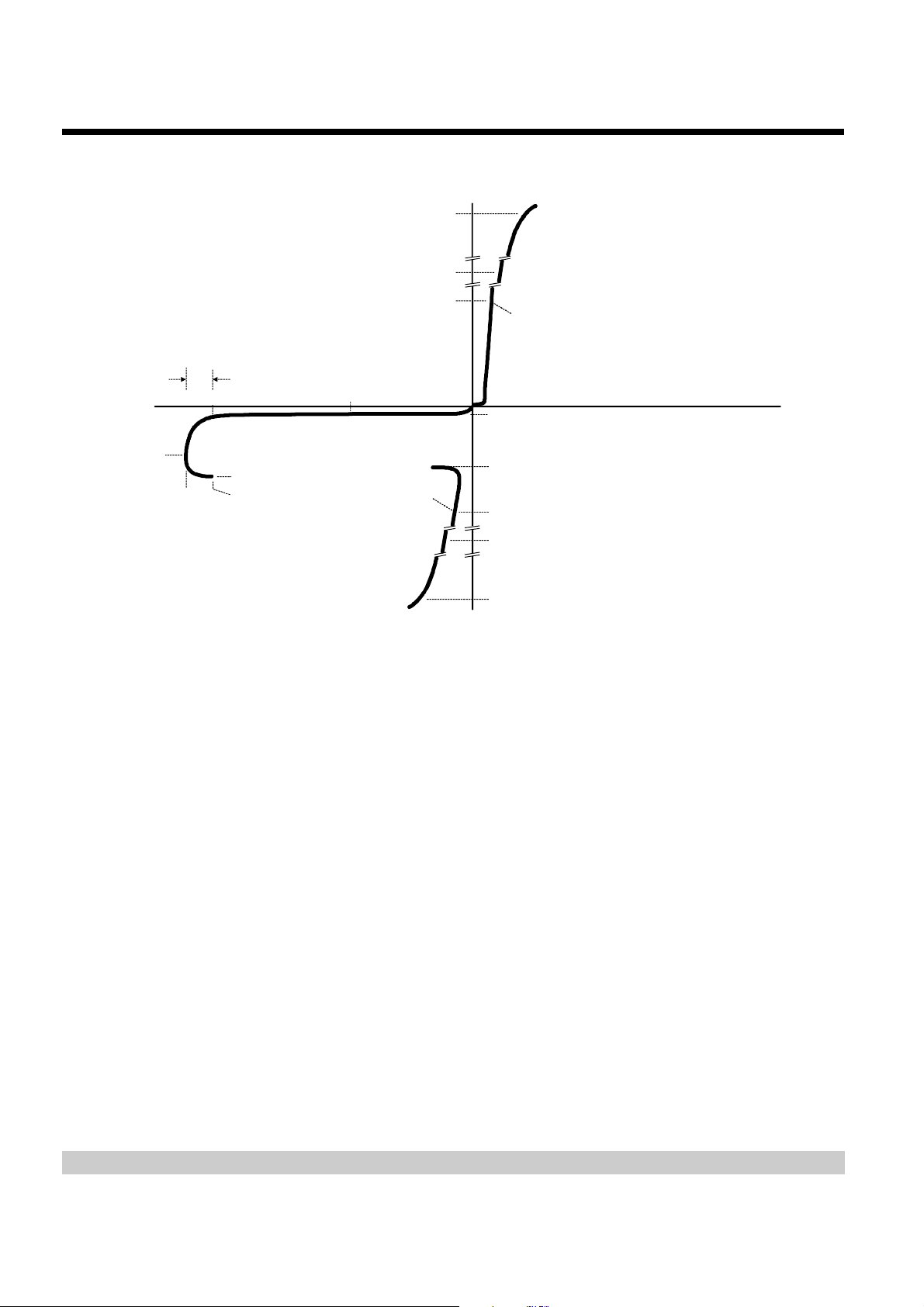
PARAMETER MEASUREMENT INFORMATION
-v
I
(BO)
V
Quadrant III
Switching
Characteristic
V
(BO)
GK(BO)
V
+i
I
(= |I
TSP
|)
FSP
Characteristic
I
(= |I
FSM
GG
I
S
V
S
V
D
|)
TSM
I
F
V
F
I
D
I
H
V
T
I
T
I
TSM
I
TSP
-i
Quadrant I
Forward
Conduction
+v
PM6XAAA
Figure 1. VOLTAGE-CURRENT CHARACTERISTIC
PRODUCT INFORMATION
4
Page 5
DUAL FORWARD-CONDUCTING P-GATE THYRISTORS
PROGRAMMABLE OVERVOLTAGE PROTECTORS
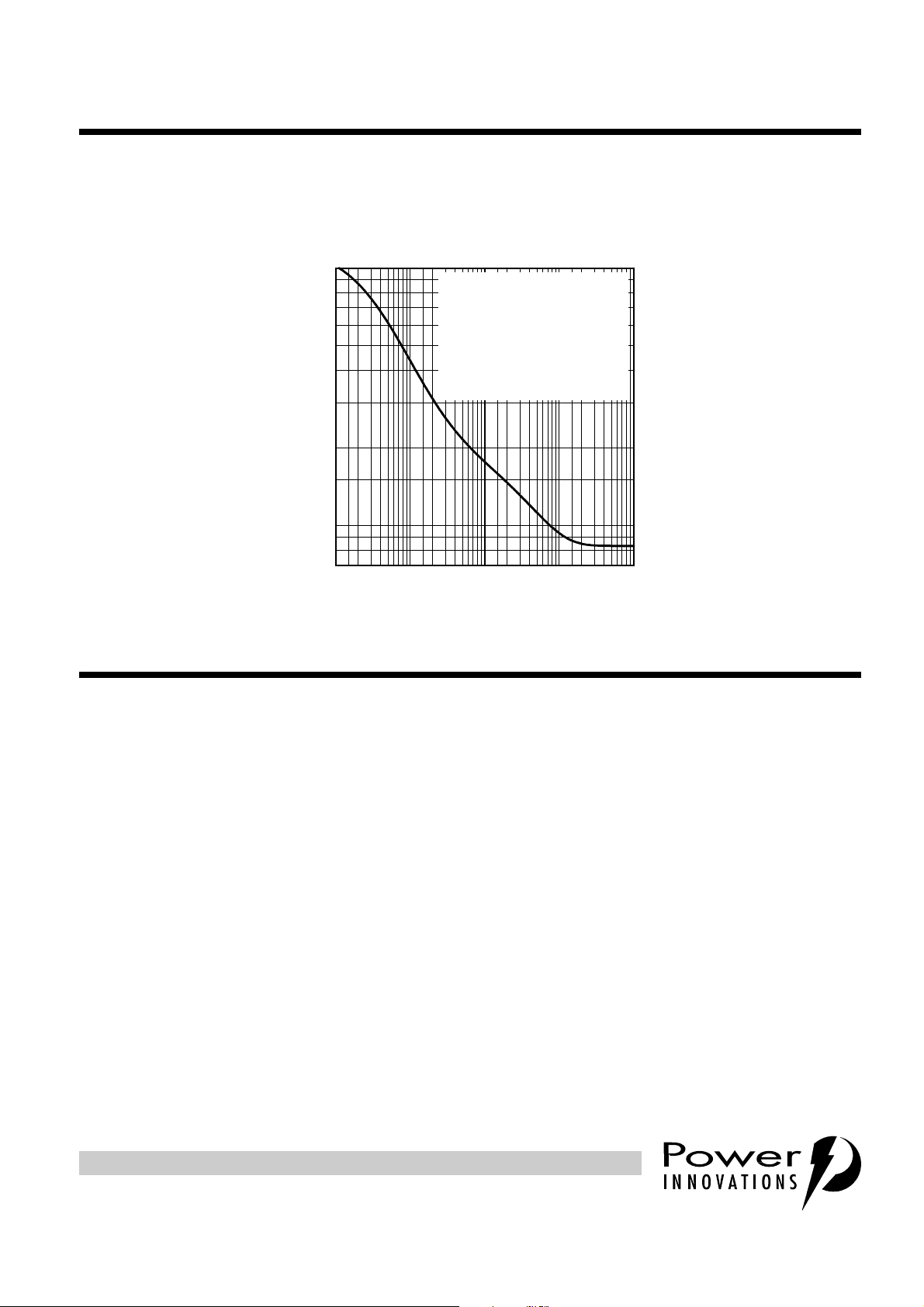
THERMAL INFORMATION
NON-REPETITIVE PEAK ON-STAT E CURRENT
vs
10
1.5
CURRENT DURATION
9
8
7
6
5
4
3
2
V
= 600 Vrms, 50/60 Hz
GEN
= 1.4*V
R
GEN
EIA/JESD51-2 ENVIRONMENT
EIA/JESD51-3 PCB
= 25 °C
T
A
GROUND RETURN = 2x
GEN
/I
TSM(t)
I
TSM(t)
TI6HAC
TISP61089A
JUNE 1999
- Non-Repetitive Peak On-State Current - A
1
0.9
TSM(t)
0.8
I
0.7
0·1 1 10 100 1000
t - Current Duration - s
Figure 2. NON-REPETITIVE PEAK ON-STATE CURRENT AGAINST DURATION
APPLICATIONS INFORMATION
gated protectors
This section covers three topics. Firstly, it is explained why gated protectors ar e n eed ed. S econd, the voltage
limiting action of the protector is described. Third, an example application circuit is described.
purpose of gated protectors
Fixed voltage thyristor overvoltage protectors have been used since the early 1980s to protect monol ithic
SLICs (Subscriber Line Interface Circuits) against overvoltages on the telephone line caused by lightning, a.c.
power contact and induction. As the SLIC was usually powered from a fixed voltage negative supply rail, the
limiting voltage of the protector could als o be a fixed value. The TISP1072F3 is a typical example of a fixed
voltage SLIC protector.
SLICs have become more sophisticated. To minimise power consumption, some designs automatically adjust
the supply voltage, V
supply voltage would be set low, but for long lines, a higher supply voltage would be generated to drive
sufficient line curre nt. The optimum protection for this type of SLIC would be given by a protection voltage
which tracks the SLIC supply voltage. This can be achieved by connecting the protection thyristor ga te to th e
SLIC supply, Figure 3. This gated (programmable) protection arrangement mi nimises the voltage stress on
the SLIC, no matter what value of supply voltage.
, to a value that is just sufficient to drive the requir ed line curre nt. For shor t lines th e
BAT
PRODUCT INFORMATION
5
Page 6
TISP61089A
DUAL FORWARD-CONDUCTING P-GATE THYRISTORS
PROGRAMMABLE OVERVOLTAGE PROTECTORS
JUNE 1999
TIP
WIRE
ΩΩΩΩ
600
GENERATOR
SOURCE
RESISTANCE
ΩΩΩΩ
600
RING
WIRE
A.C.
GENERATOR
0 - 600 Vrms
50
50
R1
R2
TISP61089A
ΩΩΩΩ
ΩΩΩΩ
Th4
Th5
C1
220 nF
SLIC
SWITCHING MODE
POWER SUPPLY
Tx
I
I
SLIC
G
I
BAT
C2
V
BAT
D1
AI6XAGA
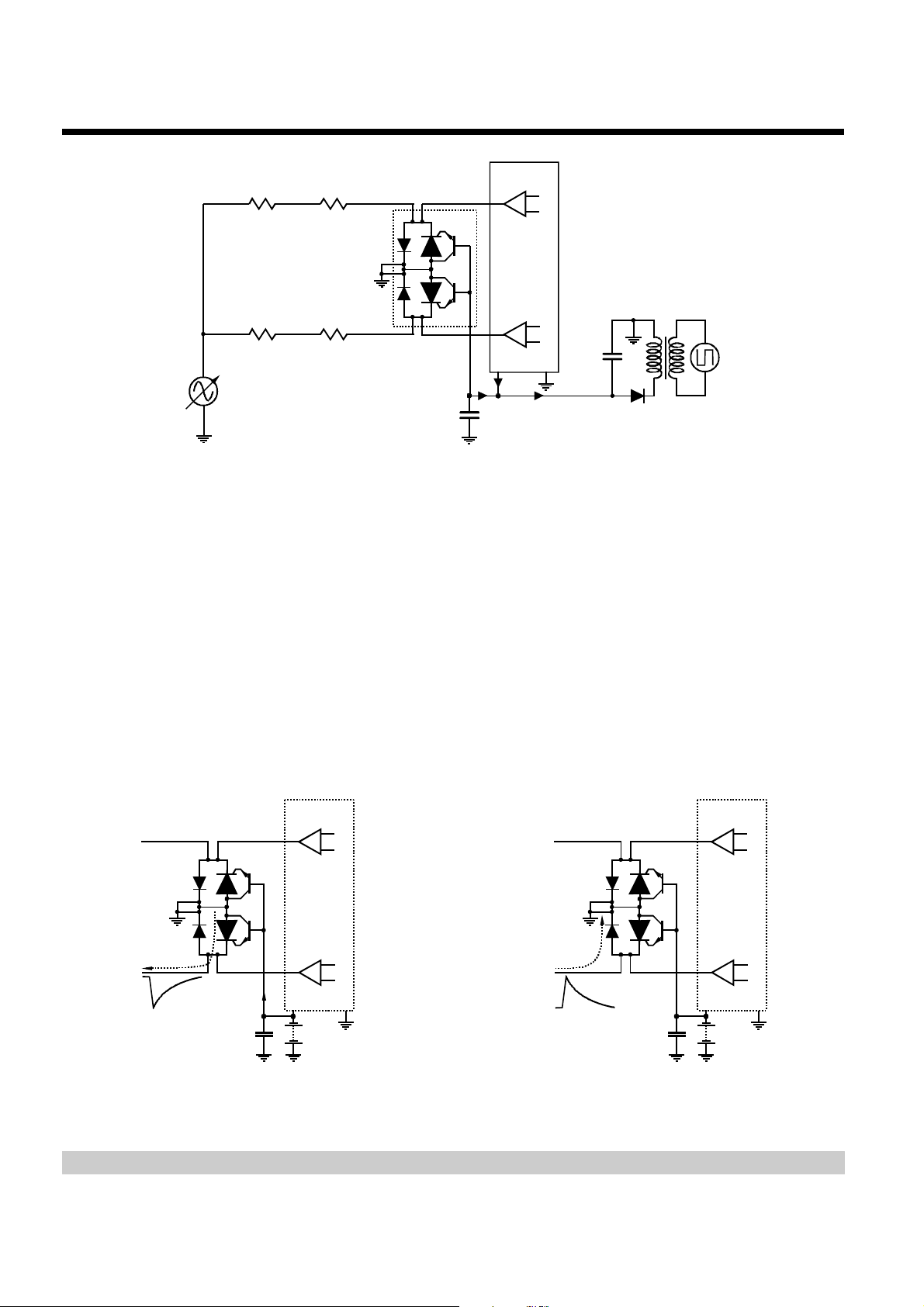
Figure 3. TISP61089A BUFFERED GATE PROTECTOR (SECTION 4.5.12 TESTING CONDITION)
operation of gated protectors
Figures 4. and 5. show how the TISP61089A limit s negati ve and positive overvoltages. Positive overvoltages
(Figure 5) are clipped by the antiparallel di odes in the TISP61089A and the resulti ng current is diverted to
ground. Negative overvoltages (Figure 4.) are initially c lipped close to the SLIC negative supply rail value
(V
). If sufficient current i s available from the overvoltage, then the protector (Th5) wil l crowbar into a low
BAT
voltage on-state conditio n. As the overvoltage subsi des th e high holding curren t of the crowbar prevents d.c.
latchup. The protection voltage will be th e sum of the gate s upply (V
(V
). The protection voltage wi ll be increased if the re i s a l ong c on nec tio n bet ween th e gate d ec oup li ng
GK(BO)
capacitor, C1, and the gate terminal. During the in iti al rise of a fast impulse, the gate cur rent ( I
as the cathode current (I
). Rates of 70 A/µs can cause inductive voltages of 0.7 V in 2.5 cm of printed wiring
K
) and the peak gate-cathode voltage
BAT
) is the same
G
track. To minimise this inductive voltage increase of protection voltage, the length of the capacit or to gate
terminal tracking should be minimised. Inductive voltages in the protector cathode wiring will also increase the
protection voltage. These voltages can be minimised by routing the SLIC connection through the protector as
shown in Figure 3.
I
K
AI6XAHA
SLIC
PROTECTOR
Th5
TISP
61089A
C1
220 nF
SLIC
I
F
I
G
V
BAT
AI6XAIA
SLIC
PROTECTOR
Th5
TISP
61089A
C1
220 nF
SLIC
V
BAT
Figure 4. NEGATIVE OVERVOLTAGE CONDITION Figure 5. POSITIVE OVERVOLTAGE CONDITION
PRODUCT INFORMATION
6
Page 7

TISP61089A
DUAL FORWARD-CONDUCTING P-GATE THYRISTORS
PROGRAMMABLE OVERVOLTAGE PROTECTORS
JUNE 1999
In Figure 6, the positive gate char ge (QGS) is about 0.1 µC which, with the 0.1 µF gate de couplin g capaci tor
used, increased the gate supply by about 1 V (= Q
volt age, V
. This increas e does not directly add to the protection voltage as the supply vo ltage change
BAT
reaches a maximum at 0.4 µs wh en the gat e curre nt reverses polarity; wher eas t he prot ection voltage peaks
at 0.3 µs. In Figure 6, the peak clamping voltage (V
supply voltage. This 5.5 V increase is the sum of the supply rail increase at that time, (0.5 V), and the
protection circuits cath ode diode to supp ly rail breakover voltage (5 V). In practice, use of the recommende d
220 nF gate decoupling capacitor would give a supply rail increase of 0.25 V and a V
-77.25 V.
0
-20
/C1). This change is just visible on the -72 V gate
GS
) is -77.5 V, an increase of 5.5 V on the nom inal gate
(BO)
value of about
(BO)
V
-40
Voltage - V
-60
-80
0.0 0.5 1.0 1.5
1
Q
GS
0
-1
-2
Current - A
-3
-4
-5
0.0 0.5 1.0 1.5
K
Time - µs
Time - µs
I
G
V
BAT
I
K
Figure 6. PROTECTOR FAST IMPULSE CLAMPING AND SWITCHING WAVEFORMS
application circuit
Figure 7 shows a typical TIS P61089A SLIC card prote ction circuit. The incoming line conductors, Ring (R)
and Tip (T), connect to the relay matrix via the series overcurrent protection. Fusible resistors, fuses and
positive temperature coefficient (PTC) r esistors can be used for overcurrent protection. Resisto rs will reduc e
the prospective current from the surge generator for both the TISP61089A and the ring/test protec tor. The
TISP7xxxF3 protector ha s the same pro tectio n voltage for any ter minal pair. This protector is use d when the
ring generator configuration may be ground or battery-backed. For dedicated ground-backed ringing
generators, the TISP3xxxF3 gives better protection as its inter-conductor protection voltage is twice the
conductor to ground value.
PRODUCT INFORMATION
7
Page 8

TISP61089A
DUAL FORWARD-CONDUCTING P-GATE THYRISTORS
PROGRAMMABLE OVERVOLTAGE PROTECTORS
JUNE 1999
TIP
WIRE
RING
WIRE
OVER-
CURRENT
PROTECTION
R1a
R1b
RING/TEST
PROTECTION
Th1
Th3
Th2
TISP
3xxxF3
OR
7xxxF3
TEST
RELAY
S1a
S1b
TEST
EQUIP-
MENT
RING
RELAY
S2a
S2b
RING
GENERATOR
SLIC
RELAY
S3a
S3b
SLIC
PROTECTOR
Th4
Th5
TISP
61089A
C1
220 nF
SLIC
V
BAT
AI6XAJA
Figure 7. TYPICAL APPLICATION CIRCUIT
Relay contacts 3a and 3b connect the line conductors to the SLIC via the TISP61089A protector. The
protector gate reference voltage comes from the SLIC negative supply (V
). A 220 nF gate capacitor
BAT
sources the high gate current pulses caused by fast rising impulses.
LSSGR 1089
GR-1089-CORE, “1089”, covers electromagnetic compatibility and electrical safety generic criteria for US
network telecommunica tion equipment. It is a module in Volume 3 of LSSGR (LATA (Local Ac cess Transport
Area) Switching Sy stems G ener ic Requ irements, FR- NWT-000064 ). In 1 089 s urge and power fault immunity
tests are done at two levels. After first-level testing the equipment shall not be damaged and shall continue to
operate correctly. Under second level testing the equipment shall not become a safety hazard. The equipment
is permitted to fail as a result of second-level testing. When the equipment is to be located on customer
premises, second-level testing incl udes a wiri ng simulator test, whic h requires the equ ipment to reduce t he
power fault current below certain values.
The following clauses reference the 1089 section a nd calculate the protector stress levels. The TISP61089A
is specified for use with a 4 0Ω series resistor. This resistor value will ensure that the TISP61089A sur vives
second level surge testing. Values down to 25Ω may be used if some second level surge failure is
acceptable. All the tabulated values are for a ser i es r esis tan ce of 40Ω. Peak current values for a 25Ω series
resistor are covered in the clause text.
The values of protector current are calculated fr om the open circuit generator voltage divide d by the sum of
the total circuit resistance. The total circuit resistance is the sum of the generator fictive source resistance and
the TISP61089A series resistor value. Most generators have multiple outputs and each output connects to an
individual line conductor. For those generators that have a single output, each conductor will have an effective
generator fictive source resistance of n times the generator fictive source resistance, where n is the number of
conductors simultaneou sl y tes ted.
PRODUCT INFORMATION
8
Page 9

TISP61089A
DUAL FORWARD-CONDUCTING P-GATE THYRISTORS
PROGRAMMABLE OVERVOLTAGE PROTECTORS
section 4.5.7 - first-level surge testing
The two most significant test wave shapes in this section are the high energy 10/1000 and the high current
2/10. As shown in table 1, the peak currents for these surges are 2x20 A and 2x56 A respectively. The
protector must sur vive the 2x20 A 10/1000 surge an d the TISP61089A will do this as its rating is 2x30 A.
When both conductors are surged simultaneously the return (anode) current will be 40 A, again the
TISP61089A will survive this as its rating for this condition will be 60 A. Similarly the TISP61089A will survive
the 2x56 A 2/10 as its rating is 2x120 A.
table 1. first-level surge currents
GENERATOR
WAVE SHAPE
2/10 2500 500 5 45 2x56
OPEN-CIRCUIT
VOLTAGE
V
SHORT-CIRCUIT
CURRENT
A
FICTIVE
SOURCE
RESISTANCE
Ω
TOTAL CIRCUIT
RESISTANCE
Ω
JUNE 1999
I
T
A
1.2/50, 8/20
(See Text)
10/360 1000 100 10 50 2x20
10/1000 600 100 6 46 2x13
10/1000 1000 100 10 50 2x20
The highest protectio n voltage will b e for the 56 A 2/10 wave shape. Under this condit ion the average rate of
current rise will be 56/2 = 28 A/µs. The value of diode and thyristor voltage under this condition is specified in
the electrical characteristics.
Compared to TR-NWT-0010 89, Issue 1, October 1 991, GR- 1089-CORE, Issue 1, November 1994, adds th e
alternative of using the IEEE C62.41 1.2/50-8/20 combination wave generator for the 2/10 test. This generator
usually has a sin gle ou tput and a fic tive resista nce of 2Ω. The 2/10 generator has a fictive output res ista nce
5Ω, (2500/500), and GR-1089-CORE compensates for this by adding an extra 3Ω in the output of the 1.2/508/20 generator. In practice, the extra 3Ω causes the prospective short-circuit current wave shape to be similar
to the 1.2/50 open-cir cuit voltage wave shape. The TISP61089A w ill s urvive the 2x53 A 1.2/50 as i ts rating is
2x100 A.
Using a 25Ω series resistor will result in table 1. I
TISP61089A will survive these peak current values as they are lower than the TISP61089A ratings.
section 4.5.8 - second-level surge testing
This is a 2/10 wave shape test. As shown in table 2, the peak current for this surge is 2x100 A. The
TISP61089A will survive the 2x100 A 2/10 surge as its rating is 2x120 A.
2500 360 4 + 3 47 2x53
column values of 2x83, 2x78 , 2x 29, 2x 19 a nd 2x 29. Th e
T
Under this condition the average rate of current r is e will be 1 00/2 = 50 A/µs. The value of dio de and thyr istor
voltage under this condition is specified in the electrical characteristics.
Compared to TR-NWT-0010 89, Issue 1, October 1 991, GR- 1089-CORE, Issue 1, November 1994, adds th e
alternative of using the IEEE C62.41 1.2/50-8/20 combination wave generator for the 2/10 test. The 2/10
generator has a fictive output resistance 10Ω, (5000/500), and GR-1089-CORE compensates for this by
adding an extra 8Ω in the output of the 1.2/50-8/20 generator. In practice, the extra 8Ω causes the
PRODUCT INFORMATION
9
Page 10

TISP61089A
DUAL FORWARD-CONDUCTING P-GATE THYRISTORS
PROGRAMMABLE OVERVOLTAGE PROTECTORS
JUNE 1999
table 2. second-level surge current
WAVE SHAPE
2/10 5000 500 10 50 2x100
1.2/50, 8/20
(See Text)
prospective shor t-cir cuit curr ent wave shape to be similar to the 1.2/ 50 open- circuit voltage wave shape. The
TISP61089A will survive the 2x96 A 1.2/50 as its rating is 2x100 A.
Using a 25Ω series resistor will result in table 2. I
fail at these peak current values as they are higher than the TISP61089A ratings.
section 4.5.9 - Intra-building surge testing
These tests use a 2/10 wave shape. As shown in table 3, the peak currents for this test are 2x27 A and 17 A.
The TISP61089A can survive both these levels as its rating is 2x120 A.
OPEN-CIRCUIT
VOLTAGE
V
5000 420 4 + 8/conductor 52 2x96
SHORT-CIRCUIT
CURRENT
A
column values of 2x143 and 2x135. The TISP61089A may
T
GENERATOR
FICTIVE
SOURCE
RESISTANCE
Ω
TOT AL
CIRCUIT
RESISTANCE
Ω
table 3. intra-building surge currents
GENERATOR
WAVE SHAPE
OPEN-CIRCUIT
VOLTAGE
V
SHORT-CIRCUIT
CURRENT
A
FICTIVE
SOURCE
RESISTANCE
Ω
TOTAL CIRCUIT
RESISTANCE
Ω
I
T
A
I
T
A
2/10 1500 100 15 55 2x27
800 100 8 48 17
1.2/50, 8/20
(See Text)
Compared to TR-NWT-001089, Issue 1, October 1991, GR-1089-CORE , Issue 1, November 1994, the 2/10
alternative of using a CCITT Recommendation K.22 1.2/50-8/20 combination wave generator has been
changed to an IEEE C 62.41 1.2/50-8/20 gen erator. This generator usually has a singl e output and a fictive
resistance of 2Ω. The 2/10 generator has fictive output resistances of 15Ω and 8Ω. GR-1089-CORE
compensates for this by adding an extra resistances of 12Ω and 6Ω in the output of the 1.2/50-8/20
generator. In practice, this extra resistance causes the pros pective shor t-circuit current wave shape to be
similar to the 1.2/50 o pen-circui t voltage wave shape. The TISP61089A will sur vive the 2x27 A 1.2 /50 as its
rating is 2x100 A.
Using a 25Ω series resistor will result in table 3. I
will survive these peak current values as they are lower than the TISP61089A ratings.
1500 94 4 + 12/conduc-
tor
800 100 2 + 6 48 17
column values of 2x38, 24, 2x37 and 24. The TISP61089A
T
56 2x27
PRODUCT INFORMATION
10
Page 11

TISP61089A
DUAL FORWARD-CONDUCTING P-GATE THYRISTORS
PROGRAMMABLE OVERVOLTAGE PROTECTORS
section 4.5.12 - first-level power fault testing
The most significant tests are a long duration (900 s) medium current test and a higher current tests of 60 one
second power applications. As shown in table 4, the peak current s for these tests are 2x0. 37 A and 2x1.3 A
respectively. The TISP6 1089A will sur vive both these conditions as its ratings are 2x0.8 3 A and 2x4.1 A for
these time periods
table 4. first-level power fault currents
JUNE 1999
A.C.
DURATION
s
1 200 0.33 600 640 2x0.31 2x0.44
1 400 0.67 600 640 2x0.63 2x0.88
1 600 1 600 640 2x0.94 2x1.3
1 1000 1 1000 1040 2x0.96 2x1.3
900 50 0.33 150 190 2x0.26 2x0.37
900 100 0.17 590 630 2x0.16 2x0.22
Using a 25Ω series resistor will result in table 4. I
2x0.23. The TISP61089A will survive these peak current values as they are lower than the TISP61089A
ratings.
section 4.5.13 - second-level power fault testing
The two most significant test s are a long duration (900 s) medium cu rrent test and a hi gher current 5 s tes t.
As shown in table 5, the peak currents for these tests are 2x17 A and 2x7.7 A respectively. For the
TISP61089A to sur vive this test, the seri es current limiting element mus t operate within 0.01 s and 0.35 s
respectively.
OPEN-CIRCUIT
RMS VOLTAGE
V
SHORT-CIRCUIT
RMS CURRENT
A
SOURCE
RESISTANCE
Ω
column values of 2x0.45, 2x0.9, 2x1.4, 2x1.4, 2x0.4 and
TM
TOTAL CIRCUIT
RESISTANCE
Ω
I
TRMS
A
I
TM
A
table 5. second-level power fault currents
A.C.
DURATION
s
5 600 60 10 50 2x12 2x17
5 600 7 86 126 2x4.8 2x6.8
900 120 25 5 45 2x2.7 2x3.8
900 277 25 11 51 2x5.4 2x7.7
900 100 0.37 273 313 2x0.32 2x0.45
900 300 1.1 273 313 2x0.96 2x1.4
900 600 2.2 273 313 2x1.9 2x2.7
OPEN-CIRCUIT
RMS VOLTAGE
V
SHORT-CIRCUIT
CURRENT
A
SOURCE
RESISTANCE
Ω
TOTAL
CIRCUIT
RESISTANCE
Ω
I
TRMS
A
PRODUCT INFORMATION
I
TM
A
11
Page 12

TISP61089A
DUAL FORWARD-CONDUCTING P-GATE THYRISTORS
PROGRAMMABLE OVERVOLTAGE PROTECTORS
JUNE 1999
Using a 25Ω series resistor will result in table 5. ITM column values of 2x24, 2x7.7, 2x5.7, 2x11, 2x0.47, 2x1.4
and 2x2.9. The TISP61089A will probably fail for a peak current level of 2x24 A and the series current limiting
element must operate in under 0 .1 s to p revent exceeding the TISP61089A package li mit. For 2x7.7 A, t he
series current limiting element must operate within 0.35 s for TISP61089A survival.
section 4.5.15 - second-level power fault testing with wiring simulator
The purpose of this test is to en sure that the telep hone cable does not become a hazard due to excessive
current. A seri es fuse, typ e MDQ 1-6/10A, si mulates the safe current levels of a telepho ne cable. If this fuse
opens the equipment fails the test. For the equipment to pass, the equipment series overcurrent element must
reduce the curren t to below the MDQ 1-6 /10A fusing level to prevent the simulator operating. The a .c. test
voltage can range from zero to 60 0 V, whic h gives a maximum co nductor current of 10 A. Table 6 shows the
simulator fusing times for three current levels.
table 6. second-level power fault currents with MDQ 1-6/10A fuse
A.C.
DURATION
s
1000 100 5 20 60 1.7 2.4
1000 300 15 20 60 5.0 7.1 30
1000 600 30 20 60 10 14 0.7
Using a 25Ω series resis tor will result in table 6. I
operating times will be ∞, 12 s and 0.4 s respectively
For the equipment to pass thi s test, t he TISP 61089A ser ies current l imiti ng eleme nt must o perate be fore the
MDQ 1-6/10A fusing times shown in table 7.
OPEN-CIRCUIT
RMS VOLTAGE
V
SHORT-
CIRCUIT
CURRENT
A
SOURCE
RESISTANCE
Ω
column values of 2x3.1, 2x 9.4 and 2x19. Simulator
TM
TOTAL
CIRCUIT
RESISTANCE
Ω
I
TRMS
A
I
TM
A
table 7. operating times of MDQ 1-6/10A fuse
TIME TO
OPERATE
s
0.2 17
0.5 12
I
RMS
A
TIME
TO
OPEN
s
∞
19
57
10 6.8
1000 2.5
overcurrent protection
To meet ‘1089, the overcurrent protectio n must be c oordi nate d wit h the r equ irements of sections 4.5.7, 4.5 .8,
4.5.9, 4.5.12, 4.5.13, 4.5. 15 and the TISP61089A. The overcurrent protection mus t not fail in the first level
tests of sections 4.5.7, 4.5.9 and 4.5.12. Recoverable overcurrent protectors (e.g. Positive Temperature
Coefficient Resisto rs) may operate dur ing first level testing, but norm al equipm ent wor king must be restor ed
PRODUCT INFORMATION
12
Page 13

TISP61089A
DUAL FORWARD-CONDUCTING P-GATE THYRISTORS
PROGRAMMABLE OVERVOLTAGE PROTECTORS
JUNE 1999
after the test has ended. The test current levels and their duration are shown in Figure 8. First level tests have
a high source resistance and the current levels are not strongly dependent on the TISP61089A series resistor
value.
Second level tests have a low source resistan ce and the current levels are dependent on the TISP61089A
series resis tor value. The two stepped lines at the top of Fig ure 8 are for the 25Ω and 40Ω series resistor
cases. If the full current-time duration s occur the equipment will fail the wiring simulator test. The MDQ 1-6/
10A fusing characteristic is also shown in Figure 8. The TISP61089A series overcurrent protection must
operate before the MDQ 1-6/10 A fus es, so th is r ep rese nts a noth er bo und ary condi tio n in the s el ect ion o f th e
overcurrent protector.
MAXIMUM RMS CURRENT
vs
30
20
10
TIME
Second Level Tests - 25
7
5
3
2
Second Level Tests - 40
MDQ 1-6/10A Fuse
AI6XAK
ΩΩΩΩ
ΩΩΩΩ
1
0.7
0.5
Maximum RMS Current - A
0.3
0.2
0.1
0.01 0.1 1 10 100 1000
Time - s
First Level Tests - 25 & 40
ΩΩΩΩ
Figure 8. ‘1089 MAXIMUM TEST CURRENT LEVEL
Figure 9 summaris es these boundar y condition s. The highest current levels that can flow are influe nced by
the TISP61089A seri es resistance. After one second the maximum curren t-time boundary bec omes set by
the MDQ 1-6/10A fusing characteristic. Fusible overcurrent protectors cannot operate at first level current
levels.
Figure 9 shows two other curves. The lower one is the TIS P61089A rated c urrent. The overcurrent p rotector
should not allow current-time d urations greater than thi s otherwise the TIS P61089A may fail. If second level
failure is acceptable then the overcurrent protector
must
operate before the TISP61089A package limit is
reached.
The TISP61089A a.c. ratings are worse case values when the device is mounted on the EIA/JE SD51- 3 PCB
used for measuring ther mal resistance. Typical PCBs would give a 25% increase in the rated currents for
periods above 0.1 s.
PRODUCT INFORMATION
13
Page 14

TISP61089A
DUAL FORWARD-CONDUCTING P-GATE THYRISTORS
PROGRAMMABLE OVERVOLTAGE PROTECTORS
JUNE 1999
OVERCURRENT PROTECTOR OPE RAT I ON LIMITS
vs
30
Second Level Tests - 25
20
10
7
5
3
2
1
0.7
0.5
Maximum RMS Current - A
0.3
0.2
Second Level Tests - 40
ΩΩΩΩ
ΩΩΩΩ
TIME
MDQ 1-6/10A Fuse
TISP61089A Package Limit
TISP61089A Survival
First Level Tests - 25 & 40
AI6XALA
ΩΩΩΩ
0.1
0.01 0.1 1 10 100 1000
Time - s
Figure 9. OVERCURRENT PROTECTOR REQUIREMENTS
PRODUCT INFORMATION
14
Page 15

TISP61089A
DUAL FORWARD-CONDUCTING P-GATE THYRISTORS
PROGRAMMABLE OVERVOLTAGE PROTECTORS
MECHANICAL DATA
D008
plastic small-outline package
This small-outline package c onsists of a circuit mounted on a lead frame and encapsulated withi n a plastic
compound. The compound will withstand soldering temperature with no deformation, and circuit performance
characteristics will remain stable when operated in high humidity conditions. Leads require no additional
cleaning or processing when used in soldered assembly.
JUNE 1999
D008
6,20 (0.244)
5,80 (0.228)
1,75 (0.069)
1,35 (0.053)
4,00 (0.157)
3,81 (0.150)
8
1
7° NOM
3 Places
5,00 (0.197)
4,80 (0.189)
765
432
0,50 (0.020)
0,25 (0.010)
x 45°NOM
Designation per JEDEC Std 30:
PDSO-G8
5,21 (0.205)
4,60 (0.181)
0,203 (0.008)
0,102 (0.004)
0,79 (0.031)
0,28 (0.011)
ALL LINEAR DIMENSIONS ARE IN MILLIMETERS AND PARENTHETICALLY IN INCHES
NOTES: A. Leads are within 0,25 (0.010) radius of true position at maximum material condition.
B. Body dimensions do not include mold flash or protrusion.
C. Mold flash or protrusion shall not exceed 0,15 (0.006).
D. Lead tips to be planar within ±0,051 (0.002).
Pin Spacing
1,27 (0.050)
(see Note A)
6 Places
0,51 (0.020)
0,36 (0.014)
8 Places
0,229 (0.0090)
0,190 (0.0075)
PRODUCT INFORMATION
7° NOM
4 Places
1,12 (0.044)
0,51 (0.020)
4° ± 4°
MDXXAA
15
Page 16

TISP61089A
DUAL FORWARD-CONDUCTING P-GATE THYRISTORS
PROGRAMMABLE OVERVOLTAGE PROTECTORS
JUNE 1999
MECHANICAL DATA
P008
plastic dual-in-line package
This dual-in-line package consi sts of a circuit mounted on a lead frame and encap sulated within a plastic
compound. The compound will withstand soldering temperature with no deformation, and circuit performance
characteristics will remain stable when operated in high humidity conditions The package is intended for
insertion in mounting-hole rows on 7,62 (0.300) centres. Once the leads are compressed and inserted,
sufficient tension is provided to secure the package in the board during soldering. Leads require no additional
cleaning or processing when used in soldered assembly.
P008
Index
Dot
10,2 (0.400) MAX
8
1 2 3 4
7 6 5
1,78 (0.070) MAX
4 Places
Designation per JEDEC Std 30:
C
L
PDIP-T8
7,87 (0.310)
7,37 (0.290)
T.P.
6,60 (0.260)
6,10 (0.240)
C
L
5,08 (0.200)
MAX
Seating
Plane
0,51 (0.020)
MIN
3,17 (0.125)
2,54 (0.100) T.P.
6 Places
(see Note A)
ALL LINEAR DIMENSIONS ARE IN MILLIMETERS AND PARENTHETICALLY IN INCHES
NOTE A: Each pin centerline is located within 0,25 (0.010) of its true longitudinal position
0,533 (0.021)
0,381 (0.015)
8 Places
MIN
PRODUCT INFORMATION
16
105°
90°
8 Places
0,36 (0.014)
0,20 (0.008)
8 Places
MDXXABA
Page 17

TISP61089A
DUAL FORWARD-CONDUCTING P-GATE THYRISTORS
PROGRAMMABLE OVERVOLTAGE PROTECTORS
JUNE 1999
IMPORTANT NOTICE
Power Innovations Limited (PI) reserves the right to make changes to its products or to discontinue any semiconductor product
or service without notice, and advises its customers to verify, before placing orders, that the information being relied on is
current.
PI warrants performance of its semiconductor products to the specifications applicable at the time of sale in accordance with
PI's standard w arr a nty. Testing and othe r quality control te ch niq ues a r e u til ized to the extent PI deems nec es sa ry to support this
warranty. Specific testing of all parameters of each device is not necessarily performed, except those mandated by government
requirements.
PI assumes no liability for applications assistance, customer product design, software performance, or infringement of patents
or services described herein. Nor is any license, either express or implied, granted under any patent right, copyright, design
right, or other intellectual property right of PI covering or relating to any combination, machine, or process in which such
semiconductor products or services might be or are used.
PI SEMICONDUCTOR PRODUCTS ARE NOT DESIGNED, INTENDED, AUTHORISED, OR WARRANTED TO BE SUITABLE
FOR USE IN LIFE-SUPPORT APPLICATIONS, DEVICES OR SYSTEMS.
Copyright © 1999, Power Innovations Limited
PRODUCT INFORMATION
17
 Loading...