

Page 1
TISP61060D, TISP61060P
negative protection voltage is controlled by the voltage,
DUAL FORWARD-CONDUCTING P-GATE THYRISTORS
PROGRAMMABLE OVERVOLTAGE PROTECTORS
SEPTEMBER 1995 - REVISED SEPTEMBER 1997Copyright © 1997, Power Innovations Limited, UK
PROGRAMMABLE SLIC OVERVOLTAGE PROTECTION
● Dual Voltage-Programmable Protectors
- Third Generation Design using Vertical
Power Technology
- Wide -5 V to -85 V Programming Range
- High 150 mA min. Holding Current
● Reduced V
Supply Current
BAT
- Triggering Current is Typically 50x Lower
- Negative Value Power Induction Current
Removes Need for Extra Protection Diode
● Rated for LSSGR & FCC Surges
I
STANDARD WAVE SHAPE
LSSGR 10/1000 µs 30
FCC Part 68 10/160 µs 45
LSSGR 2/10 µs 50
TSP
A
● Surface Mount and Through-Hole Options
- TISP61060P for Plastic DIP
- TISP61060D for Small-Outline
- TISP61060DR for Taped and Reeled
Small-Outline
● Functional Replacements for
PART NUMBERS
TCM1030P, TCM1060P, LB1201AB TISP61060P
TCM1030D, TCM1060D, LB1201AS TISP61060D
TCM1030DR, TCM1060DR TISP61060DR
FUNCTIONAL
REPLACEMENT
(Tip)
(VS)
(Ring)
Terminal typical application names shown in
(Tip)
(VS)
(Ring)
Terminal typical application names shown in
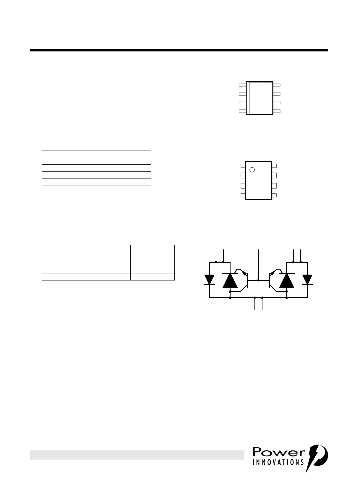
device symbol
K1 G K2
'61060D PACKAGE
(TOP VIEW)
K1
G
NC
K2
NC - No internal connection
K1
G
NC
K2
NC - No internal connection
1
2
3
4
parenthesis
'61060P PACKAGE
(TOP VIEW)
1
2
3
4 5
parenthesis
8
K1
7
A
6
A
5
K2
8
K1
A
7
A
6
K2
(Tip)
(Ground)
(Ground)
(Ring)
MD6XAO
(Tip)
(Ground)
(Ground)
(Ring)
MD6XAP
description
The TISP61060 is a dual forward-conducting
buffered p-gate overvoltage protector. It is
designed to protect monolithic SLICs (Subscriber
Line Interface Circuits), against overvoltages on
the telephone line caused by lightning, a.c.
power contact and induction. The TISP61060
Terminals K1, K2 and A correspond to the alternative
line designators of T, R and G or A, B and C. The
V
applied to the G terminal.
GG,
A
limits voltages that exceed the SLIC supply rail
voltage.
The SLIC line driver section is typically powered from 0 V (ground) and a negative voltage in the region of
-10 V to -70 V. The protector gate is connected to this negative supply. This references the protection
(clipping) voltage to the negative supply voltage. As the protection voltage will track the negative supply
voltage, the overvoltage stress on the SLIC is minimised. (see Applications Information).
Positive overvoltages are clipped to ground by diode forward conduction. Negative overvoltages are initially
clipped close to the SLIC negative supply rail value. If sufficient current is available from the overvoltage, then
the protector will crowbar into a low voltage on-state condition. As the current subsides the high holding
current of the crowbar prevents d.c. latchup.
PRODUCT INFORMATION
Information is current as of publication date. Products conform to specifications in accordance
with the terms of Power Innovations standard warranty. Production processing does not
necessarily include testing of all parameters.
SD6XAE
1
Page 2

TISP61060D, TISP61060P
DUAL FORWARD-CONDUCTING P-GATE THYRISTORS
PROGRAMMABLE OVERVOLTAGE PROTECTORS
SEPTEMBER 1995 - REVISED SEPTEMBER 1997
These monolithic protection devices are fabricated in ion-implanted planar vertical power structures for high
reliability and in normal system operation they are virtually transparent. The buffered gate design reduces the
loading on the SLIC supply during overvoltages caused by power cross and induction.
absolute maximum ratings
RATING SYMBOL VALUE UNIT
Repetitive peak off-state voltage, I
Repetitive peak gate-cathode voltage, V
= 0, -40°C ≤ TJ≤ 85°C V
G
= 0, -40°C ≤ TJ≤ 85°C V
KA
Non-repetitive peak on-state pulse current(see Notes 1 and 2)
10/1000 µs 30
10/160 µs 45
2/10 µs 50
Non-repetitive peak on-state current (see Notes 1 and 2)
I
60 Hz sine-wave, 2 s 1
Continuous on-state current (see Note 2) I
Continuous forward current (see Note 2) I
Operating free-air temperature range T
Storage temperature range T
Lead temperature 1,6 mm (1/16 inch) from case for 10 s T
DRM
GKRM
I
TSP
TSM
TM
FM
A
stg
L
-100 V
-85 V
0.3 A
0.3 A
-40 to +85 °C
-40 to +150 °C
260 °C
A
Arms 60 Hz sine-wave, 25 ms 6
NOTES: 1. Initially the protector must be in thermal equilibrium with -40°C ≤ TJ≤ 85°C. The surge may be repeated after the device returns to
its initial conditions.
2. The rated current values may be applied either to the Ring to Ground or to the Tip to Ground terminal pairs. Additionally, both
terminal pairs may have their rated current values applied simultaneously (in this case the Ground terminal current will be twice the
rated current value of an individual terminal pair). Above 85°C, derate linearly to zero at 150°C lead temperature.
recommended operating conditions
MIN TYP MAX UNIT
Gate decoupling capacitor 100 nF
C
G
electrical characteristics, -40°C ≤ TJ ≤ 85°C (unless otherwise noted)
PARAMETER TEST CONDITIONS MIN TYP MAX UNIT
T
= 25°C 5 µA
I
D
Off-state current VD= -85 V, VGK= 0 V
dv/dt = -250 V/ms, Source Resistance = 300
V
(BO)
I
S
V
T
V
F
I
H
Breakover voltage
Switching current dv/dt = -250 V/ms, Source Resistance = 300 Ω, VGG= -50 V -100 mA
On-state voltage
Forward voltage
Holding current IT= -1 A, di/dt = +1A/ms, VGG= -50 V -150 mA
dv/dt = -250 V/ms, Source Resistance = 300
= 12.5 A, 10/1000 µs, Source Resistance = 80 Ω, VGG= -50 V
I
T
I
= 1 A
T
= 10 A
I
T
= 16 A
I
T
= 30 A
I
T
I
= 1 A
F
= 10 A
I
F
= 16 A
I
F
= 30 A
I
F
J
= 85°C 50 µA
T
J
Ω, VGG= -50 V
Ω, VGG= -65 V
-53
-68
-55
V
3
4
V
5
7
2
4
V
5
5
PRODUCT INFORMATION
2
Page 3
TISP61060D, TISP61060P
DUAL FORWARD-CONDUCTING P-GATE THYRISTORS
PROGRAMMABLE OVERVOLTAGE PROTECTORS
SEPTEMBER 1995 - REVISED SEPTEMBER 1997
electrical characteristics, -40°C ≤ TJ ≤ 85°C (unless otherwise noted) (continued)
PARAMETER TEST CONDITIONS MIN TYP MAX UNIT
T
= 25°C 5 µA
I
GAS
I
GT
dv/dt
C
O
Gate reverse current VGG= -85 V, K and A terminals connected
Gate trigger current IT= -1 A, t
Critical rate of rise of
off-state voltage
Anode-cathode off-
state capacitance
= -50 V, (see Note 3) -1000 V/µs
V
GG
f = 1 MHz, V
≥ 20 µs, VGG= -50 V 15 mA
p(g)
= 0.1 V, IG= 0, (see Note 4)
d
J
= 85°C 50 µA
T
J
V
= 0 V 85 pF
D
= -50 V 10 pF
V
D
NOTES: 3. Linear rate of rise, maximum voltage limited to 80% V
4. These capacitance measurements employ a three terminal capacitance bridge incorporating a guard circuit. The unmeasured
device terminals are a.c. connected to the guard terminal of the bridge.
thermal characteristics
PARAMETER TEST CONDITIONS MIN TYP MAX UNIT
P
Junction to free air thermal resistance
R
θJA
tot
5 cm
PARAMETER MEASUREMENT INFORMATION
I
(= |I
FSP
I
(= |I
FSM
V
GK(BO)
.
GG
= 0.8 W,TA= 25°C
2
, FR4 PCB
+i
|)
TSP
|)
TSM
I
F
D Package 170
P Package 125
°C/W
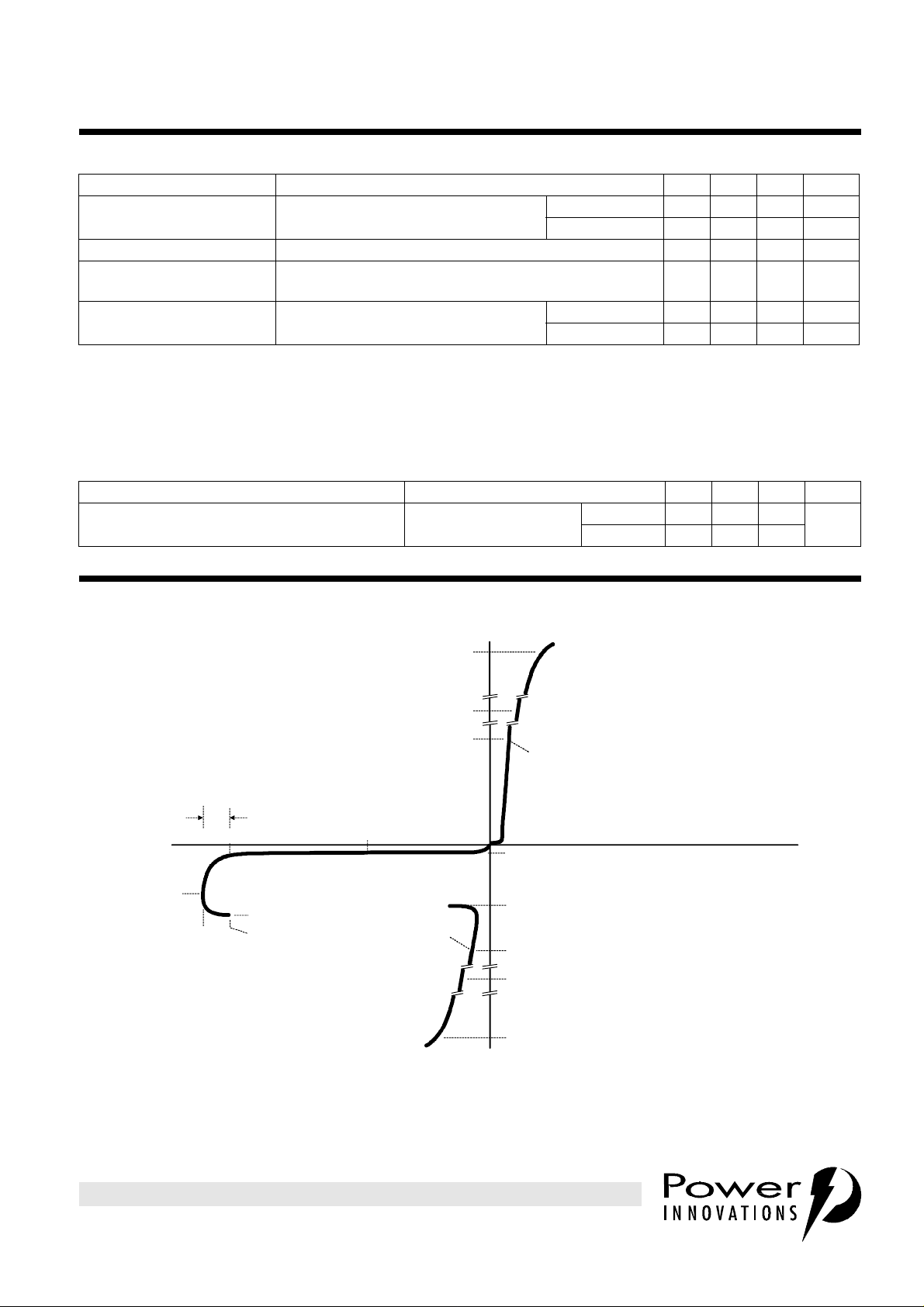
Quadrant I
Forward
Conduction
Characteristic
V
F
V
-v
I
(BO)
GG
I
S
V
(BO)
V
S
V
D
Quadrant III
Switching
Characteristic
Figure 1. VOLTAGE-CURRENT CHARACTERISTIC
PRODUCT INFORMATION
I
D
I
H
V
T
I
T
I
TSM
I
TSP
-i
+v
PM6XAAA
3
Page 4

TISP61060D, TISP61060P
DUAL FORWARD-CONDUCTING P-GATE THYRISTORS
PROGRAMMABLE OVERVOLTAGE PROTECTORS
SEPTEMBER 1995 - REVISED SEPTEMBER 1997
DEVICE PARAMETERS
general
Thyristor based overvoltage protectors, for telecommunications equipment, became popular in the late
1970s. These were fixed voltage breakover triggered devices, likened to solid state gas discharge tubes. As
these were new forms of thyristor, the existing thyristor terminology did not cover their special characteristics.
This resulted in the invention of new terms based on the application usage and device characteristic. Initially,
there was a wide diversity of terms to describe the same thing, but today the number of terms have reduced
and stabilised.
Programmable, (gated), overvoltage protectors are relatively new and require additional parameters to
specify their operation. Similarly to the fixed voltage protectors, the introduction of these devices has resulted
in a wide diversity of terms to describe the same thing. To help promote an understanding of the terms and
their alternatives, this section has a list of alternative terms and the parameter definitions used for this data
sheet. In general, the Texas Instruments approach is to use terms related to the device internal structure,
rather than its application usage as a single device may have many applications each using a different
terminology for circuit connection.
alternative symbol cross-reference guide
This guide is intended to help the translation of alternative symbols to those used in this data sheet. As in
some cases the alternative symbols have no substance in international standards and are not fully defined by
the originators, users must confirm symbol equivalence. No liability will be assumed from the use of this
guide.
CROSS-REFERENCE FOR TISP61060 AND TCM1030/60
TISP61060 PARAMETER
RATINGS & CHARACTERISTICS TCM1060, TCM1030
Non-repetitive peak on-state pulse current I
Non-repetitive peak on-state current I
Non-repetitive peak on-state current I
Forward voltage V
Forward current I
On-state voltage V
On-state current I
Switching current I
Breakover voltage V
Gate reverse current (with A and K terminals connected) I
Off-state current I
Off-state voltage V
Gate-cathode breakover voltage V
Gate voltage, (V
to the A terminal)
Off-state capacitance C
Cathode 1 K1 Tip Tip
Cathode 2 K2 Ring Ring
Anode A GND Ground
Gate G V
is gate supply voltage referenced
GG
TERMINALS TCM1060, TCM1030
DATA SHEET
SYMBOL
TSP
TSM TSM -
F
F
T
T
S
(BO)
GAS
D
D
GK(BO)
V
G
O
ALTERNATIVE
SYMBOL
- Non-repetitive peak surge current
V
CF
I
FM
V
C
I
TM
I
trip
V
trip
I
D
I
D
V
S
V
OS
V
S
C
off
S
ALTERNATIVE PARAMETER
Non-repetitive peak surge current,10 ms
Continuous 60-Hz sinewave, 2 s
Forward clamping voltage
Peak forward current
Reverse clamping voltage
Peak reverse current
Trip current
Trip voltage
Stand-by current, TIP & RING at GND
Stand-by current, TIP & RING at V
Supply voltage
Transient overshoot voltage
Supply voltage
Off-state capacitance
Supply voltage
S
PRODUCT INFORMATION
4
Page 5

DUAL FORWARD-CONDUCTING P-GATE THYRISTORS
PROGRAMMABLE OVERVOLTAGE PROTECTORS
SEPTEMBER 1995 - REVISED SEPTEMBER 1997
CROSS-REFERENCE FOR TISP61060 AND LB1201AB
TISP61060 PARAMETER
RATINGS & CHARACTERISTICS LB1201AB
Non-repetitive peak on-state pulse current I
Non-repetitive peak on-state current I
On-state voltage V
Switching current I
Breakover voltage V
Maximum continuous on-state current I
Maximum continuous forward current I
Gate voltage, (V
to the A terminal)
Off-state capacitance C
Cathode 1 K1 Tip Tip
Cathode 2 K2 Ring Ring
Anode A GND Ground
Gate G V
is gate supply voltage referenced
GG
TERMINALS LB1201AB
DATA SHEET
SYMBOL
TSP
TSM
T
S
(BO)
TM
FM
V
G
O
ALTERNATIVE
SYMBOL
I
P
I
P
V
ON
I
t
V
T
I
C
I
C
V
S
C
OFF
S
ALTERNATIVE PARAMETER
Pulse current
RMS pulse current, 60 Hz
On-state voltage
Trip current
Trip voltage
On-state current
On-state current
Supply voltage
Off-state capacitance
Supply voltage
TISP61060D, TISP61060P
APPLICATIONS INFORMATION
electrical characteristics
The electrical characteristics of a thyristor overvoltage protector are strongly dependent on junction
temperature, T
. Hence a characteristic value will depend on the junction temperature at the instant of
J
measurement. The values given in this data sheet were measured on commercial testers, which generally
minimise the temperature rise caused by testing.
gated protector evolution and characteristics
This section covers three topics. Firstly, it is explained why gated protectors are needed. Second, the
performance of the original IC (integrated circuit) based version is described. Third, the performance
improvements given by the TISP61060 are detailed.
purpose of gated protectors
Fixed voltage thyristor overvoltage protectors have been used since the early 1980s to protect monolithic
SLICs (Subscriber Line Interface Circuits) against overvoltages on the telephone line caused by lightning, a.c.
power contact and induction. As the SLIC was usually powered from a fixed voltage negative supply rail, the
limiting voltage of the protector could also be a fixed value. The TISP1072F3 is a typical example of a fixed
voltage SLIC protector.
SLICs have become more sophisticated. To minimise power consumption, some designs automatically adjust
the supply voltage, V
supply voltage would be set low, but for long lines, a higher supply voltage would be generated to drive
sufficient line current. The optimum protection for this type of SLIC would be given by a protection voltage
which tracks the SLIC supply voltage. This can be achieved by connecting the protection thyristor gate to the
SLIC supply, Figure 2. This gated (programmable) protection arrangement minimises the voltage stress on
the SLIC, no matter what value of supply voltage.
, to a value that is just sufficient to drive the required line current. For short lines the
BAT
PRODUCT INFORMATION
5
Page 6

TISP61060D, TISP61060P
DUAL FORWARD-CONDUCTING P-GATE THYRISTORS
PROGRAMMABLE OVERVOLTAGE PROTECTORS
SEPTEMBER 1995 - REVISED SEPTEMBER 1997
TIP
WIRE
ΩΩ
600
GENERATOR
SOURCE
RESISTANCE
ΩΩ
600
RING
WIRE
A.C.
GENERATOR
0 - 600 Vrms
50
50
R1
ΩΩ
R2
ΩΩ
IC BASED
SLIC
PROTECTOR
Th4
Th5
C1
100 nF
SLIC
SWITCHING MODE
POWER SUPPLY
Tx
C2
V
D2
BAT
D1
AI6XAD
I
SLIC
I
G
I
BAT
Figure 2. SIMPLIFIED IC BASED SLIC PROTECTOR CIRCUIT
ic based protectors
In 1986, an IC based gated protector was proposed (A 90 V Switching Regulator and Lightning Protection
Chip Set, Robert K. Chen, Thomas H. Lerch, Johnathan S. Radovsky, D. Alan Spires, IEEE Solid-State
Circuits Conference, February 20, 1986, pp 178/9 and pp 340/1). Commercially, this resulted in the AT&T
Microelectronics LB1201AB device and the higher current Texas Instruments Inc. TCM1060 device
This implementation consisted of four diodes and two high holding current thyristors. Positive overvoltages on
the line wires are clipped to ground by forward conduction of the wire to ground diodes. Negative
overvoltages are initially clipped close to the SLIC negative supply rail, V
, by conduction of the thyristor
BAT
cathode-gate and gate series diode. This means that the protection voltage level for slow wave forms will be
about 1.5 V lower than the SLIC supply voltage. If sufficient current is available from the overvoltage, then the
thyristor will switch into a low voltage on-state condition. When the thyristor crowbars, the two series gate
diodes prevent the SLIC supply from being shorted to ground via the thyristor gate. As the overvoltage
subsides the high holding current of the crowbar prevents d.c. latchup (see Figure 1).
impulse protection performance
The impulse protection voltage will be the sum of the gate supply (V
voltage (V
). Capacitor C1 provides the pulse of gate current that occurs during fast rising impulses.
GK(BO)
) and the impulse peak gate-cathode
BAT
The protection voltage will be increased if there is a long connection between the gate decoupling capacitor,
C1, and the gate terminal. During the initial rise of a fast impulse (e.g. 2/10), the gate current (I
as the cathode current (I
). Rates of 70 A/µs can cause inductive voltages of 0.7 V in 2.5 cm of printed wiring
K
) is the same
G
track. To minimise this inductive voltage increase of protection voltage, the length of the capacitor to gate
terminal tracking should be minimised. Inductive voltages in the protector cathode wiring can increase the
protection voltage. These voltages can be minimised by routing the SLIC connection through the protector as
shown in Figure 2.
a.c. protection performance
Figure 2 shows a typical a.c. power cross test circuit. A variable voltage a.c. source is applied to the line card
via 600
provide over-current protection by fusing or going high resistance under high current a.c. conditions.
Ω series resistors. On the line card there are further series resistors R1 and R2. These resistors
Figure 3 shows the gate and cathode a.c. power line cross voltage and current wave forms of the IC based
protector. Positive voltages are clipped at about +1 V by diode conduction. Negative voltages are clipped to
about -52 V as the SLIC supply voltage was -50 V. Sufficient current (200 mA) was available to cause the
PRODUCT INFORMATION
6
Page 7

- Gate Current - mA
10
-10
TISP61060D, TISP61060P
DUAL FORWARD-CONDUCTING P-GATE THYRISTORS
PROGRAMMABLE OVERVOLTAGE PROTECTORS
SEPTEMBER 1995 - REVISED SEPTEMBER 1997
0
-20
-30
Voltage - V
-40
-50
-60
750
500
250
0
-250
- Cathode Current - mA
-500
K
I
-750
V
G
0 5 10 15 20
0 5 10 15 20
V
K
Time - ms
I
G
I
K
Time - ms
Figure 3. IC PROTECTOR POWER CROSS WAVE FORMS
100
75
50
25
0
-25
-50
-75
-100
AI6XAG
G
I
thyristor to switch into the low-voltage on-state condition. At the end of the negative half cycle, the thyristor
switches off when the current falls below the holding current value (300 mA). Switch-off and re-clipping at
-52 V causes a second pulse of gate current. The wire current drawn by the protector is quasi-sinusoidal
During the positive a.c. voltage period (diode clipping) there is no gate current. During the negative a.c.
voltage period there are two triangular pulses of gate current, which peak at about 80 mA. This is current
which flows into the gate terminal as indicated by the I
charges the V
supply. This would not be a problem if the V
BAT
current arrow in Figure 2. This direction of current
G
supply was a rechargeable battery.
BAT
However, often the supply is generated from a switching mode power supply or the SLIC supply feed has a
series diode which blocks reverse (charging) current flow to the battery. In these cases the supply can only
sink current in the direction shown by the I
greater than I
the value of V
G
The maximum average value of I
will increase, possibly to a level which causes destruction of the SLIC.
BAT
occurs when the thyristor only clips the voltage and the peak cathode
G
arrow in Figure 2. Unless the SLIC current, I
BAT
current is just beginning to approach the switching (I
under high source impedance conditions (e.g. 600
) value, see Figure 4. The average current is maximised
S
Ω). In the case of the LB1201AB, it is recommended that
, is equal or
SLIC
the supply should be able to absorb 700 mA of “wrong way” current. If the supply cannot absorb the current
then a shunt breakdown diode is recommended to provided a path for the gate current to ground (D2 in
Figure 2). High power diodes are expensive, so diode D2 is usually low power, purposely selected to fail
under this a.c. condition and protect the SLIC.
PRODUCT INFORMATION
7
Page 8

TISP61060D, TISP61060P
Time - ms
I
K
- Cathode Current - mA
I
G
- Gate Current - mA
Voltage - V
DUAL FORWARD-CONDUCTING P-GATE THYRISTORS
PROGRAMMABLE OVERVOLTAGE PROTECTORS
SEPTEMBER 1995 - REVISED SEPTEMBER 1997
10
0
-10
-20
-30
-40
-50
-60
0 5 10 15 20
300
200
100
0
-100
-200
-300
0 5 10 15 20
V
G
Time - ms
I
K
V
K
100
80
I
G
60
40
20
0
-20
-40
-60
-80
-100
AI6XAH
Figure 4. IC PROTECTOR HIGH IMPEDANCE POWER CROSS CLIPPING WAVE FORMS
GENERATOR
RESISTANCE
GENERATOR
0 - 600 Vrms
TISP61060 buffered gate protector
The TISP61060 improves on the original IC based design in three ways, Figure 5. Firstly, the thin lateral IC
structure has been changed to a vertical power device structure for increased area efficiency and greater
ΩΩ
600
SOURCE
ΩΩ
600
A.C.
TIP
WIRE
RING
WIRE
50
50
R1
R2
TISP61060
Th4
ΩΩ
ΩΩ
Th5
C1
100 nF
SLIC
I
I
SLIC
G
I
BAT
Figure 5. TISP61060 BUFFERED GATE PROTECTOR
SWITCHING MODE
POWER SUPPLY
Tx
C2
V
BAT
D1
AI6XAE
PRODUCT INFORMATION
8
Page 9

TISP61060D, TISP61060P
Time - ms
I
K
- Cathode Current - mA
I
G
- Gate Current - mA
Voltage - V
DUAL FORWARD-CONDUCTING P-GATE THYRISTORS
PROGRAMMABLE OVERVOLTAGE PROTECTORS
SEPTEMBER 1995 - REVISED SEPTEMBER 1997
10
0
-10
V
-20
-30
-40
-50
-60
0 5 10 15 20
300
200
100
0
-100
-200
-300
0 5 10 15 20
V
G
Time - ms
I
K
I
G
K
I
G
I
K
10
8
6
4
2
0
-2
-4
-6
-8
-10
AI6XAI
Figure 6. TISP61060 HIGH IMPEDANCE POWER CROSS CLIPPING WAVE FORMS
energy capability. Second, the series gate diodes have been changed to transistor buffers. The maximum
current injected into the gate supply is then reduced by the transistors gain factor (H
). Third, some current
FE
from the positive voltage diode conduction has been diverted to the gate terminal which subtracts from the
normal gate current. In most cases, this allows any previously used SLIC supply rail shunt protection diode to
be removed. Although the SLIC supply is taken to a terminal that is internally connected to transistor bases,
the terminal is still designated as the gate terminal, G.
Figure 6 shows the high impedance a.c. waveforms for the TISP61060. As the TISP61060 replaces the IC
based protector’s gate diode with a transistor, the peak gate current is reduced by over 50 times. In addition
there is a compensating negative gate current flow during diode conduction. The TISP61060 has the
maximum value of peak gate current specified and so allows for designer to design for limit conditions. Most
IC protectors do not specify this parameter. Figure 7 shows the improvement due to the TISP61060. These
plots show the full cycle average gate current against rms a.c. voltage. The IC based protector has a
substantial positive gate current which will always charge the SLIC supply, possibly causing an overvoltage.
The TISP61060 has a negative gate current and so cannot overvoltage the SLIC.
PRODUCT INFORMATION
9
Page 10

TISP61060D, TISP61060P
- RMS Supply Voltage - V
I
G(AV)
- Average Gate Current - mA
DUAL FORWARD-CONDUCTING P-GATE THYRISTORS
PROGRAMMABLE OVERVOLTAGE PROTECTORS
SEPTEMBER 1995 - REVISED SEPTEMBER 1997
25
Figure 4. Condition
20
Protector Starting to Crowbar
15
Figure 3. Condition
10
Figure 2. and Figure 5.
Test Circuits
5
0
-5
Figure 6. Condition
-10
0 100 200 300 400 500
V
AC
IC Based Protector
TISP61060
AI6XAJ
Figure 7. AVERAGE GATE CURRENT VS A.C. SUPPLY VOLTAGE IN FIGURES 2 AND 5
circuit component values
The TISP61060 is a functional replacement for three devices, the LB1201, TCM1030 and TCM1060. These
devices have a minimum value of series limiting resistor (R1 and R2 in Figure 2) which will ensure that the
impulse surge current will not exceed the device rated value. This is summarised in the table below.
RECCOMMENDED
MIN. SERIES
RESISTANCE
100
LB1201
DEVICE
RESISTANCE
10/1000
1 kV, 10
I
A 12.5 18.5 23
TSP
MIN. SERIES
Ω
Ω
70 73.6 104
10/160
1.5 kV, 7.5 Ω
2/10
2.5 kV, 5 Ω
Ω
A 16 25 35
I
TSP
TCM1030
TCM1060
TISP61060
MIN. SERIES
RESISTANCE
A 30 45 50
I
TSP
MIN. SERIES
RESISTANCE
A 30 45 50
I
TSP
MIN. SERIES
RESISTANCE
Ω
Ω
Ω
52.5 52.5 66.4
23.3 25.8 45
23.3 25.8 45
100
50
50
This table shows that the TISP61060 has impulse ratings which are higher or equal to those of the other three
devices. Similarly, the TISP61060 has a.c. ratings which are higher or equal to those of the other three
devices. A series over-current protector should be included in the wire feed to prevent exceeding the
PRODUCT INFORMATION
10
Page 11

TISP61060D, TISP61060P
DUAL FORWARD-CONDUCTING P-GATE THYRISTORS
PROGRAMMABLE OVERVOLTAGE PROTECTORS
SEPTEMBER 1995 - REVISED SEPTEMBER 1997
TISP61060 a.c. ratings. As covered earlier, the gate decoupling capacitor should be 100 nF and should be
mounted as close to the protector as possible.
application circuit
Figure 8 shows a typical TISP61060 SLIC card protection circuit. The incoming line wires, R and T, connect to
the relay matrix via the series over-current protection. Fusible resistors, fuses and positive temperature
coefficient (PTC) resistors can be used for over-current protection. Resistors will reduce the prospective
current from the surge generator for both the TISP61060 and the ring/test protector. The TISP7xxxF3
protector has the same protection voltage for any terminal pair. This protector is used when the ring generator
configuration maybe ground or battery-backed. For dedicated ground-backed ringing generators, the
TISP3xxxF3 gives better protection as its inter-wire protection voltage is twice the wire to ground value.
TIP
WIRE
RING
WIRE
OVER-
CURRENT
PROTECTION
R1
R2
RING/TEST
PROTECTION
Th3
Th2
TISP
3xxxF3
OR
7xxxF3
Th1
TEST
RELAY
S1a
S1b
TEST
EQUIP-
MENT
RING
RELAY
S2a
S2b
RING
GENERATOR
SLIC
RELAY
S3a
S3b
SLIC
PROTECTOR
Th4
Th5
TISP
61060
100 nF
SLIC
V
BAT
AI6XAF
Figure 8. TYPICAL APPLICATION CIRCUIT
Relay contacts 3a and 3b connect the line wires to the SLIC via the TISP61060 protector. The protector gate
reference voltage comes from the SLIC negative supply (V
). A 100 nF gate capacitor sources the high
BAT
gate current pulses caused by fast rising impulses.
PRODUCT INFORMATION
11
Page 12

TISP61060D, TISP61060P
D. Lead tips to be planar within ±0,051 (0.002).
DUAL FORWARD-CONDUCTING P-GATE THYRISTORS
PROGRAMMABLE OVERVOLTAGE PROTECTORS
SEPTEMBER 1995 - REVISED SEPTEMBER 1997
MECHANICAL DATA
D008
plastic small-outline package
This small-outline package consists of a circuit mounted on a lead frame and encapsulated within a plastic
compound. The compound will withstand soldering temperature with no deformation, and circuit performance
characteristics will remain stable when operated in high humidity conditions. Leads require no additional
cleaning or processing when used in soldered assembly.
D008
6,20 (0.244)
5,80 (0.228)
1,75 (0.069)
1,35 (0.053)
4,00 (0.157)
3,81 (0.150)
8
1
7° NOM
3 Places
5,00 (0.197)
4,80 (0.189)
7 6 5
0,50 (0.020)
0,25 (0.010)
432
x 45°NOM
Designation per JEDEC Std 30:
PDSO-G8
5,21 (0.205)
4,60 (0.181)
0,203 (0.008)
0,102 (0.004)
0,79 (0.031)
0,28 (0.011)
ALL LINEAR DIMENSIONS ARE IN MILLIMETERS AND PARENTHETICALLY IN INCHES
NOTES: A. Leads are within 0,25 (0.010) radius of true position at maximum material condition.
B. Body dimensions do not include mold flash or protrusion.
C. Mold flash or protrusion shall not exceed 0,15 (0.006).
PRODUCT INFORMATION
12
Pin Spacing
1,27 (0.050)
(see Note A)
6 Places
0,51 (0.020)
0,36 (0.014)
8 Places
0,229 (0.0090)
0,190 (0.0075)
7° NOM
4 Places
1,12 (0.044)
0,51 (0.020)
4° ± 4°
MDXXAA
Page 13

TISP61060D, TISP61060P
NOTE A: Each pin centerline is located within 0,25 (0.010) of its true longitudinal position
DUAL FORWARD-CONDUCTING P-GATE THYRISTORS
PROGRAMMABLE OVERVOLTAGE PROTECTORS
SEPTEMBER 1995 - REVISED SEPTEMBER 1997
MECHANICAL DATA
P008
plastic dual-in-line package
This dual-in-line package consists of a circuit mounted on a lead frame and encapsulated within a plastic
compound. The compound will withstand soldering temperature with no deformation, and circuit performance
characteristics will remain stable when operated in high humidity conditions The package is intended for
insertion in mounting-hole rows on 7,62 (0.300) centers. Once the leads are compressed and inserted,
sufficient tension is provided to secure the package in the board during soldering. Leads require no
additional cleaning or processing when used in soldered assembly.
P008
Index
Dot
10,2 (0.400) MAX
8
1 2 3 4
7 6 5
1,78 (0.070) MAX
4 Places
Designation per JEDEC Std 30:
C
L
PDIP-T8
7,87 (0.310)
7,37 (0.290)
T.P.
6,60 (0.260)
6,10 (0.240)
C
L
0,51 (0.020)
MIN
2,54 (0.100) T.P.
6 Places
(see Note A)
ALL LINEAR DIMENSIONS ARE IN MILLIMETERS AND PARENTHETICALLY IN INCHES
0,533 (0.021)
0,381 (0.015)
8 Places
PRODUCT INFORMATION
5,08 (0.200)
MAX
3,17 (0.125)
MIN
Seating
Plane
105°
90°
8 Places
0,36 (0.014)
0,20 (0.008)
8 Places
MDXXABA
13
Page 14

TISP61060D, TISP61060P
DUAL FORWARD-CONDUCTING P-GATE THYRISTORS
PROGRAMMABLE OVERVOLTAGE PROTECTORS
SEPTEMBER 1995 - REVISED SEPTEMBER 1997
IMPORTANT NOTICE
Power Innovations Limited (PI) reserves the right to make changes to its products or to discontinue any
semiconductor product or service without notice, and advises its customers to verify, before placing orders, that the
information being relied on is current.
PI warrants performance of its semiconductor products to the specifications applicable at the time of sale in
accordance with PI's standard warranty. Testing and other quality control techniques are utilized to the extent PI
deems necessary to support this warranty. Specific testing of all parameters of each device is not necessarily
performed, except as mandated by government requirements.
PI accepts no liability for applications assistance, customer product design, software performance, or infringement
of patents or services described herein. Nor is any license, either express or implied, granted under any patent
right, copyright, design right, or other intellectual property right of PI covering or relating to any combination,
machine, or process in which such semiconductor products or services might be or are used.
PI SEMICONDUCTOR PRODUCTS ARE NOT DESIGNED, INTENDED, AUTHORIZED, OR WARRANTED TO BE
SUITABLE FOR USE IN LIFE-SUPPORT APPLICATIONS, DEVICES OR SYSTEMS.
Copyright © 1997, Power Innovations Limited
PRODUCT INFORMATION
14
 Loading...