

Page 1

DatasheetArchive.com
Request For Quotation
Order the parts you need from our real-time inventory database.
Simply complete a request for quotation form with your part
information and a sales representative will respond to you with
price and availability.
Request For Quotation
Your free datasheet starts on the next page.
More datasheets and data books are available from our
homepage: http://www.datasheetarchive.com
This datasheet has been downloaded from http://www.datasheetarchive.com.
Page 2

TEA1623P; TEA1623PH
STARplug
Rev. 01 — 17 March 2004 Product data sheet
1. General description
The TEA1623P; TEA1623PH is a Switched Mode Power Supply (SMPS) controller IC that
operates directly from the rectified universal mains. It is implemented in the high voltage
EZ-HV™ SOI process, combined with a low voltage BICMOS process.
The device includes a high voltage power switch and a circuit for start-up directly from the
rectified mains voltage. A dedicated circuit for valley switching is built in, which makes a
very efficient slim-line electronic power-plug concept possible.
In its most basic version of application, the TEA1623P; TEA1623PH acts as a voltage
source. Here, no additional secondary electronics are required. A combined voltage and
current source can be realized with minimum costs for external components.
Implementation of the TEA1623P; TEA1623PH renders an efficient and low cost power
supply system.
2. Features
TM
■ Designed for general purpose supplies
■ Integrated power switch: 6.5 Ω and 650 V
■ Operates from universal AC mains supplies: 80 V to 276 V
■ Adjustable frequency for flexible design
■ RC oscillator for load insensitive regulation loop constant
■ Valley switching for minimum switch-on loss
■ Frequency reduction at low power output for low standby power: <100 mW
■ Adjustable overcurrent protection
■ Undervoltage protection
■ Temperature protection
■ Short winding protection
■ Safe restart mode for system fault conditions
■ Simple application with both primary and secondary (opto) feedback
■ Available in 8-pin and 16-pin DIP package.
3. Applications
■ Adapters ■ VCD
■ Set-Top Box (STB) ■ CD(R)
■ DVD ■ PC Silverbox standby SMPS.
Page 3

Philips Semiconductors
4. Quick reference data
Table 1: Quick reference data
Symbol Parameter Conditions Min Typ Max Unit
V
CC(max)
V
DRAIN(max)
I
DRAIN
R
DSon
f
osc
T
amb
5. Ordering information
TEA1623P; TEA1623PH
STARplug
maximum supply voltage - - 40 V
maximum voltage at pin
DRAIN
supply current drawn from
pin DRAIN
drain-source on-state
resistance
oscillator frequency range 10 - 200 kHz
ambient temperature −20 - +85 °C
Tj>0°C - - 650 V
no auxiliary supply - 0.5 - mA
I
SOURCE
= −0.5 A
=25°C - 6.5 7.5 Ω
T
j
= 100 °C - 9.0 10.0 Ω
T
j
TM
Table 2: Ordering information
Type number Package
Name Description Version
TEA1623P DIP8 plastic dual in-line package; 8 leads (300 mil) SOT97-1
TEA1623PH DIP16 plastic dual in-line package; 16 leads (300 mil);
SOT38-1
long body
9397 750 12579 © Koninklijke Philips Electronics N.V. 2004. All rights reserved.
Product data sheet Rev. 01 — 17 March 2004 2 of 18
Page 4
Philips Semiconductors
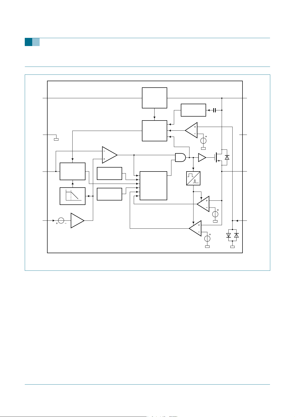
6. Block diagram
TEA1623P; TEA1623PH
STARplug
TM
V
CC
GND
RC
REG
1
2
stop
3
OSCILLATOR
low frequency
f
2.5 V
4
1.8 U
10x
TEA1623P
PWM
THERMAL
SHUTDOWN
POWER-UP
RESET
SUPPLY
LOGIC
PROTECTION
LOGIC
overcurrent
short winding
VALLEY
blank
100 mV
0.5 V
8
7
6
5
DRAIN
n.c.
SOURCE
AUX
0.75 V
col011
Fig 1. Block diagram of TEA1623P.
9397 750 12579 © Koninklijke Philips Electronics N.V. 2004. All rights reserved.
Product data sheet Rev. 01 — 17 March 2004 3 of 18
Page 5
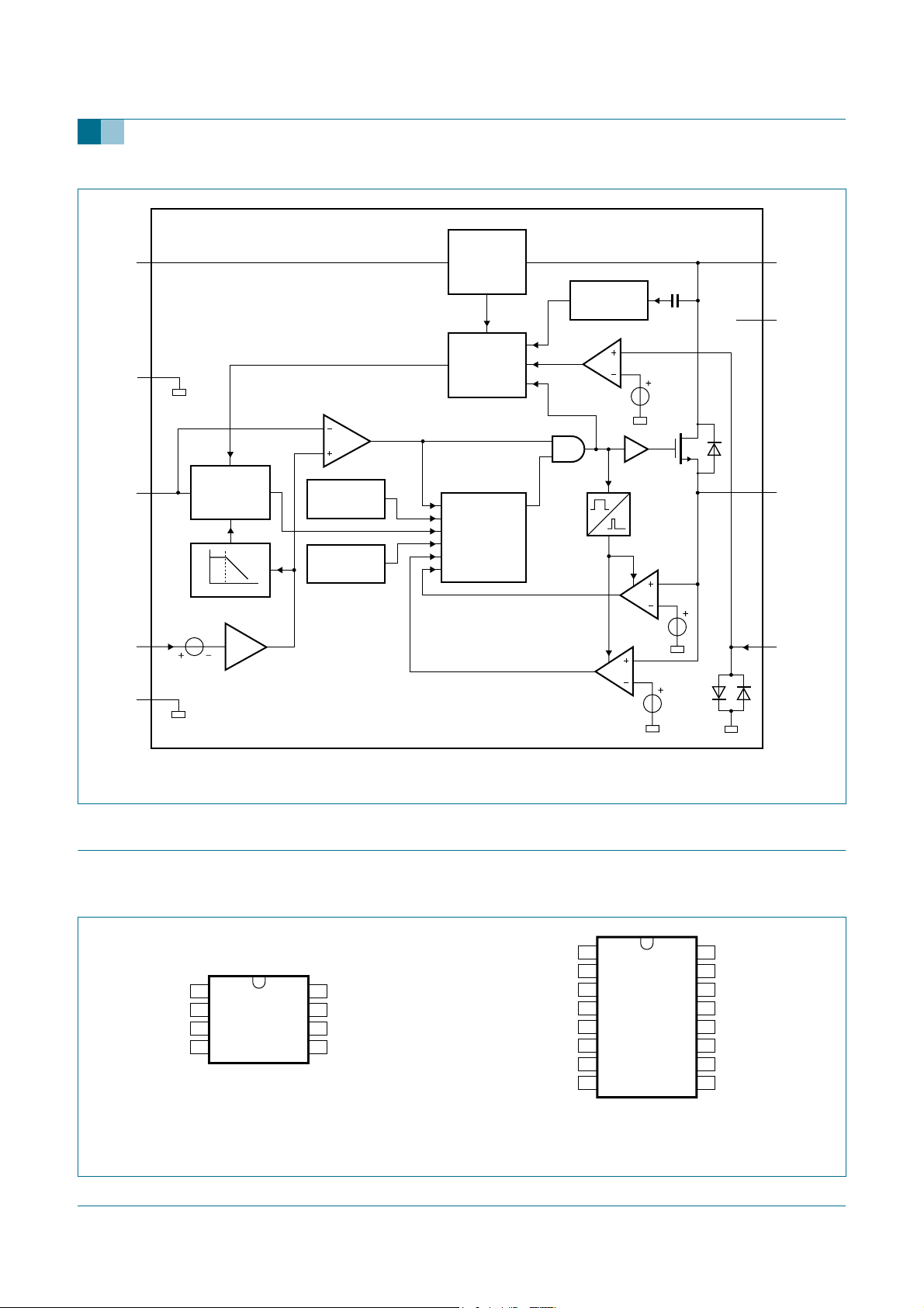
Philips Semiconductors
TEA1623P; TEA1623PH
STARplug
TM
V
CC
GND
RC
REG
SGND
3
4
stop
5
OSCILLATOR
low frequency
f
2.5 V
6
8
1.8 U
10x
TEA1623PH
PWM
THERMAL
SHUTDOWN
POWER-UP
RESET
SUPPLY
LOGIC
PROTECTION
LOGIC
overcurrent
short winding
VALLEY
blank
0.75 V
100 mV
0.5 V
1, 2, 7, 9,
10, 13,
15, 16
14
DRAIN
n.c.
12
SOURCE
11
AUX
col013
Fig 2. Block diagram of TEA1623PH.
7. Pinning information
7.1 Pinning
n.c. n.c.
1
n.c. n.c.
2
V
V
1
CC
GND n.c.
2
3
4
TEA1623P
001aaa310
RC SOURCE
REG AUX
8
7
6
5
DRAIN
3
CC
GND n.c.
4
RC SOURCE
REG AUX
n.c. n.c.
SGND n.c.
TEA1623PH
5
6
7
8
001aaa312
a. DIP8 package. b. DIP16 package.
Fig 3. Pin configuration.
9397 750 12579 © Koninklijke Philips Electronics N.V. 2004. All rights reserved.
Product data sheet Rev. 01 — 17 March 2004 4 of 18
16
15
14
13
12
11
10
DRAIN
9
Page 6

Philips Semiconductors
7.2 Pin description
Table 3: Pin description
Symbol Pin Description
V
CC
GND 2 4 ground
RC 3 5 frequency setting
REG 4 6 regulation input
SGND - 8 signal ground; must preferably be connected to pin GND
AUX 5 11 input for voltage from auxiliary winding for timing
SOURCE 6 12 source of internal MOS switch
n.c. 7 1,2, 7, 9, 10,
DRAIN 8 14 drain of internal MOS switch; input for start-up current
TEA1623P; TEA1623PH
TEA1623P TEA1623PH
1 3 supply voltage
(demagnetization)
not connected
13, 15, 16
and valley sensing
STARplug
TM
8. Functional description
The TEA1623P; TEA1623PH is the heart of a compact flyback converter, with the IC
placed at the primary side. The auxiliary winding of the transformer can be used for
indirect feedbackto control the isolated output. This additional winding also powers the IC.
A more accurate control of the output voltage and/or current can be implemented with an
additional secondary sensing circuit and optocoupler feedback.
The TEA1623P; TEA1623PH uses voltage mode control. The frequency is determined by
the maximum transformer demagnetizing time and the time of the oscillator. In the first
case, the converter operates in the Self Oscillating Power Supply (SOPS) mode. In the
latter case, it operates at a constant frequency, which can be adjusted with external
components RRC and CRC. This mode is called Pulse Width Modulation (PWM).
Furthermore, a primary stroke is started only in a valley of the secondary ringing. This
valley switching principle minimizes capacitive switch-on losses.
8.1 Start-up and undervoltage lock-out
Initially, the IC is self supplying from the rectified mains voltage. The IC starts switching as
soon as the voltage on pin VCCpasses the V
auxiliary winding of the transformer as soon as VCC is high enough and the supply from
the line is stopped for high efficiency operation.
As soon as the voltage on pin VCC drops below the V
and restarts from the rectified mains voltage.
CC(start)
level. The supply is taken over by the
level, the IC stops switching
CC(stop)
8.2 Oscillator
The frequency of the oscillator is set by the external resistor and capacitor on pin RC. The
external capacitor is charged rapidly to the V
stroke, it discharges to the V
level. Because the discharge is exponential, the
RC(min)
RC(max)
relative sensitivity of the duty factor to the regulation voltage at low duty factor is almost
9397 750 12579 © Koninklijke Philips Electronics N.V. 2004. All rights reserved.
Product data sheet Rev. 01 — 17 March 2004 5 of 18
leveland, starting from a new primary
Page 7

Philips Semiconductors
equal to the sensitivity at high duty factors. This results in a more constant gain over the
duty factor range compared to PWM systems with a linear sawtooth oscillator. Stable
operation at low duty factors is easily realized. For high efficiency, the frequency is
reduced as soon as the duty factor drops below a certain value. This is accomplished by
increasing the oscillator charge time.
To ensure that the capacitor can be charged within the charge time, the value of the
oscillator capacitor should be limited to approximately 1 nF.
8.3 Duty factor control
The duty factor is controlled by the internal regulation voltage and the oscillator signal on
pin RC. The internal regulation voltage is equal to the external regulation voltage (minus
2.5 V) multiplied by the gain of the error amplifier (typical 20 dB or 10 ×).
The minimum duty factor of the switched mode power supply is 0 %. The maximum duty
factor is set to 75 % (typical value at 100 kHz oscillation frequency).
8.4 Valley switching
TEA1623P; TEA1623PH
STARplug
TM
A new cycle is started at the primary stroke when the switch is switched on (see Figure 4).
After a certain time (determined by the RC oscillator voltage and the internal regulation
level), the switch is turned off and the secondary stroke starts. The internal regulation
level is determined by the voltage on pin REG. After the secondary stroke, the drain
voltage shows an oscillation with a frequency of approximately
Where:
Lp is the primary self inductance on the drain node
Cp is the parasitic capacitance on the drain node.
As soon as the oscillator voltage is high again and the secondary stroke has ended, the
circuit waits for a low drain voltage before starting a new primary stroke.
The primary stroke starts some time before the actual valley at low ringing frequencies,
and some time after the actual valley at high ringing frequencies. Figure 5 shows a typical
curve for a reflected voltage N × Vo of 80 V. This voltage is the output voltage Vo (see
Figure 6) transferred to the primary side of the transformer with the factor N (determined
by the turns ratio of the transformer). Figure 5 shows that the system switches exactly at
minimum drain voltage for ringing frequencies of 480 kHz, thus reducing the switch-on
losses to a minimum. At 200 kHz, the next primary stroke is started at 33° before the
valley. The switch-on losses are still reduced significantly.
1
------------------------------
2π LpC
×
p
9397 750 12579 © Koninklijke Philips Electronics N.V. 2004. All rights reserved.
Product data sheet Rev. 01 — 17 March 2004 6 of 18
Page 8

Philips Semiconductors
TEA1623P; TEA1623PH
STARplug
TM
primary
stroke
drain
valley
secondary
stroke
RC
oscillator
regulation level
A: Start of new cycle with valley switching.
B: Start of new cycle in a classical PWM system.
Fig 4. Signals for valley switching.
secondary
stroke
secondary
ringing
A
B
col007
40
phase
(°)
20
0
−20
−40
0 800600200 400
Reflected voltage at N × Vo=80V.
Fig 5. Typical phase of drain ringing at switch-on.
001aaa311
f (kHz)
9397 750 12579 © Koninklijke Philips Electronics N.V. 2004. All rights reserved.
Product data sheet Rev. 01 — 17 March 2004 7 of 18
Page 9

Philips Semiconductors
8.5 Demagnetization
The system operates in discontinuous conduction mode all the time. As long as the
secondary stroke has not ended, the oscillator will not start a new primary stroke. During
the suppression time t
may be necessary in applications where the transformer has a large leakage inductance
and at low output voltages.
8.6 Protections
8.6.1 Overcurrent protection
The cycle-by-cycle peak drain current limit circuit uses the external source resistor RI(see
Figure 6) to measure the current. The circuit is activated after the leading edge blanking
time t
leb
primary peak current.
8.6.2 Short winding protection
The short winding protection circuit is also activated after the leading edge blanking time.
If the source voltage exceeds the short winding protection voltage V
TEA1623PH stops switching. Only a power-on reset will restart normal operation. The
short winding protection also protects in case of a secondary diode short circuit.
TEA1623P; TEA1623PH
, demagnetization recognition is suppressed. This suppression
suppr
. The protection circuit limits the source voltage to V
source(max)
STARplug
, and thus limits the
, the TEA1623P;
swp
TM
8.6.3 Overtemperature protection
An accurate temperature protection is provided in the TEA1623P; TEA1623PH. When the
junction temperature exceeds the thermal shutdown temperature, the IC stops switching.
During thermal protection, the IC current is lowered to the start-up current. The IC
continues normal operation as soon as the overtemperature situation has disappeared.
8.6.4 Overvoltage protection
Overvoltage protection can be achieved in the application by pulling pin REG above its
normal operation level, or by keeping the level of pin AUX above V
primary stroke is terminated immediately, and no new primary stroke is started until the
voltage on pin REG drops to its normal operation level. Pin REG has an internal clamp.
The current feed into pin REG must be limited.
8.7 Characteristics of the complete power-plug
8.7.1 Input
The input voltage range comprises the universal AC mains from 80 V to 276 V.
8.7.2 Accuracy
The accuracy of the complete converter, functioning as a voltage source with primary
sensing, is approximately 8 % (mainly dependent on the transformer coupling). The
accuracy with secondary sensing is defined by the accuracy of the external components.
For safety requirements in case of optocoupler feedback loss, the primary sensing
remains active when an overvoltage circuit is connected.
. The current
demag
9397 750 12579 © Koninklijke Philips Electronics N.V. 2004. All rights reserved.
Product data sheet Rev. 01 — 17 March 2004 8 of 18
Page 10

Philips Semiconductors
8.7.3 Efficiency
An efficiency of 75 % at maximum output power can be achievedfor a complete converter
designed for universal mains.
8.7.4 Ripple
A minimum ripple is obtained in a system designed for a maximum duty factor of 50 %
under normal operating conditions, and a minimized dead time. The magnitude of the
ripple in the output voltage is determined by the frequency and duty factor of the
converter, the output current level, and the value and ESR of the output capacitor.
9. Limiting values
Table 4: Limiting values
In accordance with the Absolute Maximum Rating System (IEC 60134).
Symbol Parameter Conditions Min Max Unit
Voltages
V
CC
V
RC
V
SOURCE
V
DRAIN
Currents
I
REG
I
AUX
I
RC
I
SOURCE
I
DRAIN
General
P
tot
T
stg
T
amb
T
j
V
esd
TEA1623P; TEA1623PH
STARplug
supply voltage continuous
oscillator input voltage
DMOS power transistor source
voltage
DMOS power transistor drain
voltage
regulation input current
auxiliary winding input current
oscillator capacitor charge
current
source current −2+2A
drain current −2+2A
total power dissipation
TEA1623P T
TEA1623PH T
<45°C - 1.0 W
amb
<50°C - 1.7 W
amb
storage temperature −55 +150 °C
ambient temperature −20 +85 °C
junction temperature −20 +145 °C
electrostatic discharge voltage human body model
pin DRAIN −1500 +1500 V
all other pins −2000 +2000 V
machine model
all pins −200 +200 V
[1]
−0.4 +40 V
[1]
−0.4 +3 V
−0.4 +5 V
−0.4 +650 V
[2]
-6mA
[2]
−10 +5 mA
−3- mA
[3]
[4]
TM
[1] Pins VCC and RC are not allowed to be current driven.
[2] Pins REG and AUX are not allowed to be voltage driven.
[3] Human body model: equivalent to discharging a 100 pF capacitor through a 1.5 kΩ series resistor.
9397 750 12579 © Koninklijke Philips Electronics N.V. 2004. All rights reserved.
Product data sheet Rev. 01 — 17 March 2004 9 of 18
Page 11

Philips Semiconductors
[4] Machine model: equivalent to discharging a 200 pF capacitor through a 0.75 µH coil and a 10 Ω series
resistor.
10. Thermal characteristics
Table 5: Thermal characteristics
Symbol Parameter Conditions Typ Unit
R
th(j-a)
thermal resistance from junction to
ambient
TEA1623P 100 K/W
TEA1623PH 55 K/W
TEA1623P; TEA1623PH
TM
in free air
STARplug
[1]
[1] Thermal resistance R
printed-circuit board. See the TEA152x application notes for details.
can be lower when pin GND is connected to sufficient copper area on the
th(j-a)
11. Characteristics
Table 6: Characteristics
T
=25°C; no overtemperature; all voltages are measured with respect to ground; currents are positive when flowing into
amb
the IC; unless otherwise specified.
Symbol Parameter Conditions Min Typ Max Unit
Supplies
Supply on pin V
V
CC(start)
V
CC(stop)
I
CC(operate)
I
CC(startup)
I
CC(ch)
Supply on pin DRAIN
I
DRAIN
Pulse width modulator mode
δ
min
δ
max
Self oscillating power supply mode
V
demag
t
suppr
Oscillator: pin RC
V
RC(min)
V
RC(max)
CC
start voltage 9 9.5 10 V
stop voltage undervoltage lock-out 7.0 7.5 8.0 V
operating supply current normal operation - 1.3 1.9 mA
start-up supply current start-up - 180 400 µA
charging current V
>60V
DRAIN
=0V −650 −520 −390 µA
V
CC
= 8.5 V −375 −275 −175 µA
V
CC
supply current drawn from pin DRAIN no auxiliary supply - 0.5 - mA
with auxiliary supply;
>60V
V
DRAIN
- 30 125 µA
minimum duty factor - 0 - %
maximum duty factor f
demagnetization recognition voltage
= 100 kHz - 75 - %
osc
50 100 150 mV
level
time of suppression of transformer
1.0 1.5 2.0 µs
ringing at start of secondary stroke
minimum voltage of RC oscillator
60 75 90 mV
setting
maximum voltage of RC oscillator
2.4 2.5 2.6 V
setting
9397 750 12579 © Koninklijke Philips Electronics N.V. 2004. All rights reserved.
Product data sheet Rev. 01 — 17 March 2004 10 of 18
Page 12

Philips Semiconductors
TEA1623P; TEA1623PH
STARplug
TM
Table 6: Characteristics
T
=25°C; no overtemperature; all voltages are measured with respect to ground; currents are positive when flowing into
amb
…continued
the IC; unless otherwise specified.
Symbol Parameter Conditions Min Typ Max Unit
t
RC(ch)
f
osc
RC charging time - 1 - µs
oscillator frequency range 10 - 200 kHz
Duty factor regulator: pin REG
V
REG
G
V(erroramp)
V
REG(clamp)
input voltage on pin REG 2.4 2.5 2.6 V
voltage gain of error amplifier - 20 - dB
clamping voltage on pin REG I
= 6 mA - - 7.5 V
REG
Valley switching recognition
dV/dt
valley
f
valley
t
d(valley-on)
valley recognition −102 - +102 V/µs
ringing frequency for valley switching N × Vo= 100 V 200 550 800 kHz
delay from valley recognition to
- 150 - ns
switch-on
Output stage (FET)
I
L(drain)
V
BR(drain)
R
DSon
t
drain(f)
drain leakage current V
drain breakdown voltage Tj>0°C 650 - - V
drain-source on-state resistance I
drain fall time V
= 650 V - - 125 µA
DRAIN
SOURCE
= −0.5 A
=25°C - 6.5 7.5 Ω
T
j
= 100 °C - 9.0 10.0 Ω
T
j
DRAIN(switch_on)
= 300 V;
-75-ns
no external capacitor at pin
DRAIN
Temperature protection
T
prot(max)
T
prot(hys)
maximum threshold temperature 150 160 170 °C
threshold temperature hysteresis - 2 - °C
Overcurrent and short winding protection: pin SOURCE
V
source(max)
V
swp
t
d(propagation)
overcurrent protection voltage dV/dt = 0.1 V/µs 0.47 0.50 0.53 V
short winding protection voltage dV/dt = 0.5 V/µs 0.7 0.75 0.8 V
delay from detecting V
source(max)
to
dV/dt = 0.5 V/µs - 160 185 ns
switch-off
t
leb
leading edge blanking time both overcurrent and short
250 350 450 ns
winding protection
9397 750 12579 © Koninklijke Philips Electronics N.V. 2004. All rights reserved.
Product data sheet Rev. 01 — 17 March 2004 11 of 18
Page 13

Philips Semiconductors
12. Application information
TEA1623P; TEA1623PH
STARplug
TM
LF
CF1
mains
R1
R4
R3
CF2
C
VCC
GND
R
RC
C
RC
REG
Further application information can be found in the TEA152x application notes.
Fig 6. Application with primary sensing for TEA1623P.
13. Test information
V
CC
RC
R2
1
2
TEA1623P
3
4
D2
DRAIN
8
n.c.
7
SOURCE
6
AUX
5
Z1
D1
D5
C5
C6 - Ycap
R
I
R
AUX
col012
V
o
13.1 Quality information
The
General Quality Specification for Integrated Circuits, SNW-FQ-611
9397 750 12579 © Koninklijke Philips Electronics N.V. 2004. All rights reserved.
Product data sheet Rev. 01 — 17 March 2004 12 of 18
is applicable.
Page 14

Philips Semiconductors
14. Package outline
TEA1623P; TEA1623PH
STARplug
TM
DIP8: plastic dual in-line package; 8 leads (300 mil)
D
seating plane
A
L
Z
e
b
8
pin 1 index
1
w M
b
1
b
2
5
SOT97-1
M
E
A
2
A
c
(e )
1
M
H
E
1
DIMENSIONS (inch dimensions are derived from the original mm dimensions)
A
A
12
min.
max.
050G01 MO-001 SC-504-8
b
1.73
1.14
0.068
0.021
0.045
0.015
IEC JEDEC JEITA
mm
OUTLINE
VERSION
SOT97-1
A
max.
UNIT
inches
Note
1. Plastic or metal protrusions of 0.25 mm (0.01 inch) maximum per side are not included.
b
0.53
0.38
4
0 5 10 mm
scale
1
1.07
0.89
0.042
0.035
b
2
0.36
0.23
0.014
0.009
REFERENCES
(1) (1)
cD E e M
9.8
9.2
0.39
0.36
6.48
6.20
0.26
0.24
1
3.60
3.05
0.14
0.12
E
8.25
7.80
0.32
0.31
EUROPEAN
PROJECTION
10.0
0.39
0.33
M
L
e
H
8.3
w
max.
0.2542.54 7.62
1.154.2 0.51 3.2
0.010.1 0.3
0.0450.17 0.02 0.13
ISSUE DATE
99-12-27
03-02-13
(1)
Z
Fig 7. Package outline DIP8.
9397 750 12579 © Koninklijke Philips Electronics N.V. 2004. All rights reserved.
Product data sheet Rev. 01 — 17 March 2004 13 of 18
Page 15

Philips Semiconductors
TEA1623P; TEA1623PH
STARplug
TM
DIP16: plastic dual in-line package; 16 leads (300 mil); long body
D
seating plane
L
Z
16
pin 1 index
e
b
b
1
9
A
w M
SOT38-1
M
E
A
2
A
1
c
(e )
1
M
H
E
1
0 5 10 mm
DIMENSIONS (inch dimensions are derived from the original mm dimensions)
A
A
A
UNIT
inches
Note
1. Plastic or metal protrusions of 0.25 mm (0.01 inch) maximum per side are not included.
mm
OUTLINE
VERSION
SOT38-1
max.
4.7 0.51 3.7
1 2
min.
max.
1.40
1.14
0.055
0.15
0.045
IEC JEDEC JEITA
050G09 MO-001 SC-503-16
b
b
0.53
0.38
0.021
0.015
cEe M
1
0.32
0.23
0.013
0.009
REFERENCES
D
21.8
21.4
0.86
0.84
8
scale
(1) (1)
6.48
6.20
0.26
0.24
e
0.3
L
3.9
3.4
EUROPEAN
PROJECTION
M
8.25
7.80
0.32
0.31
E
9.5
8.3
0.37
0.33
1
0.15
0.13
H
w
max.
0.2542.54 7.62
0.087
0.010.10.020.19
ISSUE DATE
99-12-27
03-02-13
2.2
(1)
Z
Fig 8. Package outline DIP16.
9397 750 12579 © Koninklijke Philips Electronics N.V. 2004. All rights reserved.
Product data sheet Rev. 01 — 17 March 2004 14 of 18
Page 16

Philips Semiconductors
15. Soldering
15.1 Introduction to soldering through-hole mount packages
This text gives a brief insight to wave, dip and manual soldering. A more in-depth account
of soldering ICs can be found in our
(document order number 9398 652 90011).
Wave soldering is the preferred method for mounting of through-hole mount IC packages
on a printed-circuit board.
15.2 Soldering by dipping or by solder wave
Driven by legislation and environmental forces the worldwide use of lead-free solder
pastes is increasing. Typical dwell time of the leads in the wave ranges from
3 to 4 seconds at 250 °C or 265 °C, depending on solder material applied, SnPb or
Pb-free respectively.
The total contact time of successive solder waves must not exceed 5 seconds.
TEA1623P; TEA1623PH
STARplug
Data Handbook IC26; Integrated Circuit Packages
TM
The device may be mounted up to the seating plane, but the temperature of the plastic
body must not exceed the specified maximum storage temperature (T
printed-circuit board has been pre-heated, forced cooling may be necessary immediately
after soldering to keep the temperature within the permissible limit.
15.3 Manual soldering
Apply the soldering iron (24 V or less) to the lead(s) of the package, either below the
seating plane or not more than 2 mm aboveit. If the temperature of the soldering iron bit is
less than 300 °C it may remain in contact for up to 10 seconds. If the bit temperature is
between 300 and 400 °C, contact may be up to 5 seconds.
15.4 Package related soldering information
Table 7: Suitability of through-hole mount IC packages for dipping and wave soldering
methods
Package Soldering method
Dipping Wave
DBS, DIP, HDIP, RDBS, SDIP, SIL suitable suitable
[2]
PMFP
[1] For SDIP packages, the longitudinal axis must be parallel to the transport direction of the printed-circuit
board.
[2] For PMFP packages hot bar soldering or manual soldering is suitable.
− not suitable
stg(max)
[1]
). If the
9397 750 12579 © Koninklijke Philips Electronics N.V. 2004. All rights reserved.
Product data sheet Rev. 01 — 17 March 2004 15 of 18
Page 17

Philips Semiconductors
TEA1623P; TEA1623PH
STARplug
16. Revision history
Table 8: Revision history
Document ID Release date Data sheet status Change notice Order number Supersedes
TEA1623P_TEA1623PH_1 20040317 Product data - 9397 750 12579 -
TM
9397 750 12579 © Koninklijke Philips Electronics N.V. 2004. All rights reserved.
Product data sheet Rev. 01 — 17 March 2004 16 of 18
Page 18

Philips Semiconductors
17. Data sheet status
TEA1623P; TEA1623PH
STARplug
TM
Level Data sheet status
I Objective data Development This data sheet contains data from the objective specification for product development. Philips
II Preliminary data Qualification This data sheet contains data fromthepreliminary specification. Supplementary data will be published
III Product data Production This data sheet contains data from the product specification. Philips Semiconductors reserves the
[1] Please consult the most recently issued data sheet before initiating or completing a design.
[2] The product status of the device(s) described in this data sheet may have changed since this data sheet was published. The latest information is available on the Internet at
URL http://www.semiconductors.philips.com.
[3] For data sheets describing multiple type numbers, the highest-level product status determines the data sheet status.
[1]
Product status
18. Definitions
Short-form specification — The data in a short-form specification is
extracted from a full data sheet with the same type number and title. For
detailed information see the relevant data sheet or data handbook.
Limiting values definition — Limiting values given are in accordance with
the Absolute Maximum Rating System (IEC 60134). Stress above one or
more of the limiting values may cause permanent damage to the device.
These are stress ratings only and operation of the device at these or at any
other conditions above those given in the Characteristics sections of the
specification is not implied. Exposure to limiting values for extended periods
may affect device reliability.
Application information — Applications that are described herein for any
of these products are for illustrative purposes only. Philips Semiconductors
make no representation or warranty that such applications will be suitable for
the specified use without further testing or modification.
[2] [3]
Definition
Semiconductors reserves the right to change the specification in any manner without notice.
at a later date. Philips Semiconductors reserves the right to change the specification without notice, in
order to improve the design and supply the best possible product.
right to make changes at any time in order to improve the design, manufacturing and supply.Relevant
changes will be communicated via a Customer Product/Process Change Notification (CPCN).
customers using or selling these products for use in such applications do so
at their own risk and agree to fully indemnify Philips Semiconductors for any
damages resulting from such application.
Right to make changes — Philips Semiconductors reserves the right to
make changes in the products - including circuits, standard cells, and/or
software - described or contained herein in order to improve design and/or
performance. When the product is in full production (status ‘Production’),
relevant changes will be communicated via a Customer Product/Process
Change Notification (CPCN). Philips Semiconductors assumes no
responsibility or liability for the use of any of these products, conveys no
license or title under any patent, copyright, or mask work right to these
products, andmakes no representations or warrantiesthat these products are
free from patent, copyright,ormaskwork right infringement, unless otherwise
specified.
20. Trademarks
19. Disclaimers
Life support — These products are not designed for use in life support
appliances, devices, or systems where malfunction of these products can
reasonably be expected to result in personal injury. Philips Semiconductors
STARplug —is a trademark of Koninklijke Philips Electronics N.V.
EZ-HV — is a trademark of Koninklijke Philips Electronics N.V.
21. Contact information
For additional information, please visit: http://www.semiconductors.philips.com
For sales office addresses, send an email to: sales.addresses@www.semiconductors.philips.com
9397 750 12579 © Koninklijke Philips Electronics N.V. 2004. All rights reserved.
Product data sheet Rev. 01 — 17 March 2004 17 of 18
Page 19

Philips Semiconductors
22. Contents
1 General description. . . . . . . . . . . . . . . . . . . . . . 1
2 Features . . . . . . . . . . . . . . . . . . . . . . . . . . . . . . . 1
3 Applications . . . . . . . . . . . . . . . . . . . . . . . . . . . . 1
4 Quick reference data . . . . . . . . . . . . . . . . . . . . . 2
5 Ordering information. . . . . . . . . . . . . . . . . . . . . 2
6 Block diagram . . . . . . . . . . . . . . . . . . . . . . . . . . 3
7 Pinning information. . . . . . . . . . . . . . . . . . . . . . 4
7.1 Pinning . . . . . . . . . . . . . . . . . . . . . . . . . . . . . . . 4
7.2 Pin description . . . . . . . . . . . . . . . . . . . . . . . . . 5
8 Functional description . . . . . . . . . . . . . . . . . . . 5
8.1 Start-up and undervoltage lock-out . . . . . . . . . 5
8.2 Oscillator. . . . . . . . . . . . . . . . . . . . . . . . . . . . . . 5
8.3 Duty factor control. . . . . . . . . . . . . . . . . . . . . . . 6
8.4 Valley switching. . . . . . . . . . . . . . . . . . . . . . . . . 6
8.5 Demagnetization. . . . . . . . . . . . . . . . . . . . . . . . 8
8.6 Protections . . . . . . . . . . . . . . . . . . . . . . . . . . . . 8
8.6.1 Overcurrent protection . . . . . . . . . . . . . . . . . . . 8
8.6.2 Short winding protection. . . . . . . . . . . . . . . . . . 8
8.6.3 Overtemperature protection . . . . . . . . . . . . . . . 8
8.6.4 Overvoltage protection . . . . . . . . . . . . . . . . . . . 8
8.7 Characteristics of the complete power-plug . . . 8
8.7.1 Input . . . . . . . . . . . . . . . . . . . . . . . . . . . . . . . . . 8
8.7.2 Accuracy. . . . . . . . . . . . . . . . . . . . . . . . . . . . . . 8
8.7.3 Efficiency . . . . . . . . . . . . . . . . . . . . . . . . . . . . . 9
8.7.4 Ripple . . . . . . . . . . . . . . . . . . . . . . . . . . . . . . . . 9
9 Limiting values. . . . . . . . . . . . . . . . . . . . . . . . . . 9
10 Thermal characteristics. . . . . . . . . . . . . . . . . . 10
11 Characteristics. . . . . . . . . . . . . . . . . . . . . . . . . 10
12 Application information. . . . . . . . . . . . . . . . . . 12
13 Test information . . . . . . . . . . . . . . . . . . . . . . . . 12
13.1 Quality information . . . . . . . . . . . . . . . . . . . . . 12
14 Package outline . . . . . . . . . . . . . . . . . . . . . . . . 13
15 Soldering . . . . . . . . . . . . . . . . . . . . . . . . . . . . . 15
15.1 Introduction to soldering through-hole mount
packages . . . . . . . . . . . . . . . . . . . . . . . . . . . . 15
15.2 Soldering by dipping or by solder wave . . . . . 15
15.3 Manual soldering . . . . . . . . . . . . . . . . . . . . . . 15
15.4 Package related soldering information . . . . . . 15
16 Revision history. . . . . . . . . . . . . . . . . . . . . . . . 16
17 Data sheet status. . . . . . . . . . . . . . . . . . . . . . . 17
18 Definitions . . . . . . . . . . . . . . . . . . . . . . . . . . . . 17
19 Disclaimers. . . . . . . . . . . . . . . . . . . . . . . . . . . . 17
20 Trademarks. . . . . . . . . . . . . . . . . . . . . . . . . . . . 17
21 Contact information . . . . . . . . . . . . . . . . . . . . 17
TEA1623P; TEA1623PH
STARplug
TM
© Koninklijke Philips Electronics N.V. 2004
All rights are reserved. Reproduction in whole or in part is prohibited without the prior
written consent of the copyright owner. The information presented in this document does
not form part of any quotation or contract, is believed to be accurate and reliable and may
be changed without notice. No liability will be accepted by the publisher for any
consequence of its use. Publication thereof does not convey nor imply any license under
patent- or other industrial or intellectual property rights.
Published in The Netherlands
Date of release: 17 March 2004
Document order number: 9397 750 12579
 Loading...