

Page 1
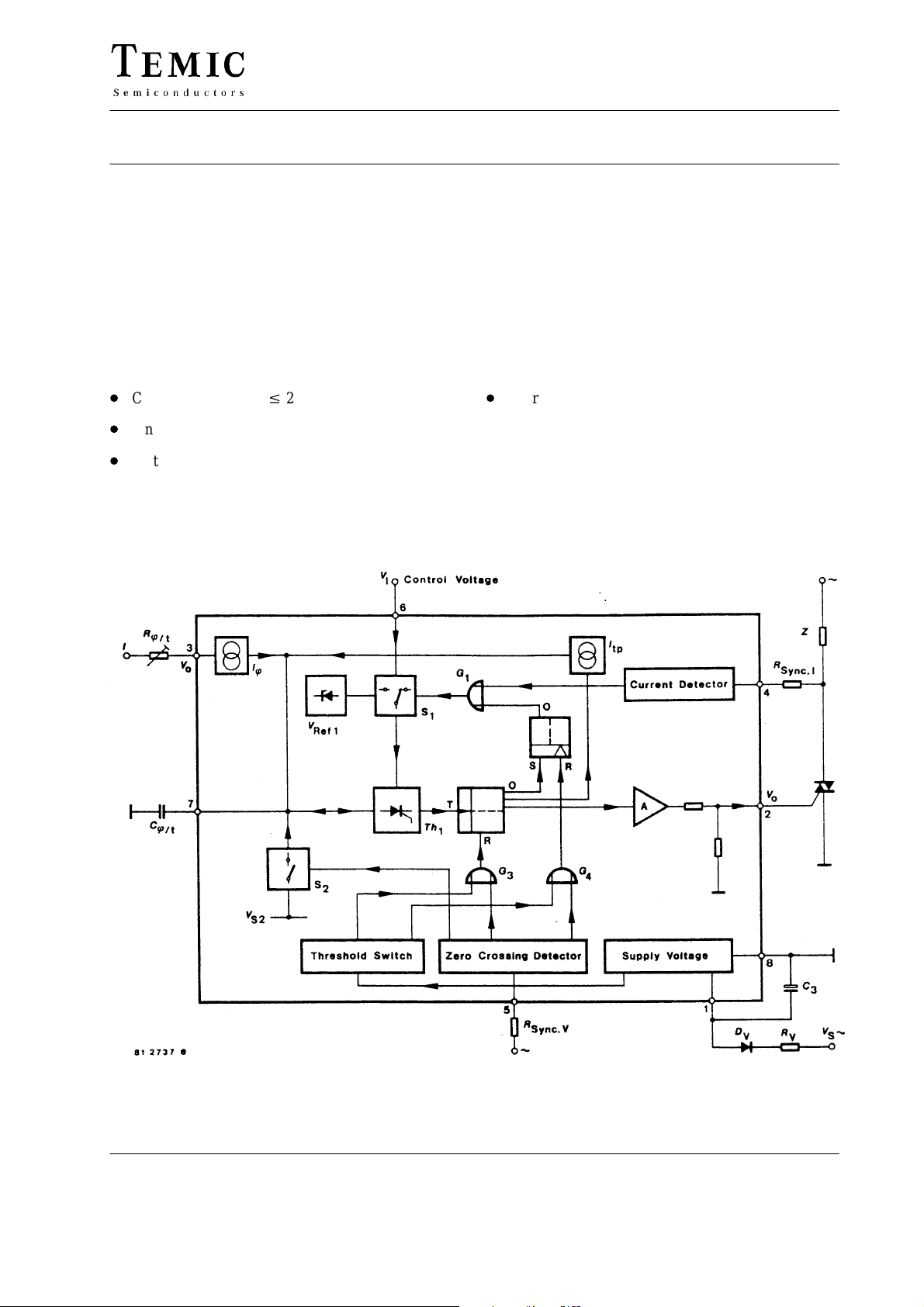
Simple Phase Control Circuit
Description
Integrated circuit, TEA1007, is designed as a general
phase control circuit in bipolar technology. It has an
internal supply voltage limitation. With typical 150 mA
ignition pulse, it is possible to determine the phase-shift
Features
D
Current consumption v 2.5 mA
D
Ignition pulse typ. 150 mA
D
Voltage and current synchronization
TEA1007
of the ignition point by comparing the mains sync. ramp
voltage with a preset required value. It generates a single
ignition pulse per half wave; therefore, it is suitable for
capacitive and inductive loads in low cost applications.
D
Internal supply voltage control
Package: DIP8
Block Diagram
R = series resistance
v
TELEFUNKEN Semiconductors
Rev . A1, 28-May-96
Figure 1. Block diagram with typical circuitry
1 (8)
Page 2
TEA1007
General Description
The phase-shift of the ignition point is determined in the
usual manner by comparison between a mains
synchronized ramp voltage and a predetermined required
value. The capacitor C
reference point Pin 8 is discharged at the zero transition
of the mains voltage via the V
switch S
. After the end of the zero transition pulse, C
2
is charged from the constant current source Iö, whose
value is adjusted externally with R
unavoidable tolerance of C
When the potential at Pin 7 reaches the nominal value
predetermined at Pin 6, the thyristor Th
functions as a comparator, ignites and sets the following
clock flip-flop. The output of the clock flip-flop releases
the output amplifier, connects a second constant current
source to the capacitor C
voltage switch S
voltage V
The capacitor C
+ Itp until it reaches the internal reference voltage
I
ö
. The length of this Phase 2 corresponds to the width
V
Ref
via an RS flip-flop and the OR gate G1.
Ref1
ö
of the output pulse t
the value V
, thyristor Th1ignites again and resets the
Ref
clock flip-flop to its initial state. The output pulse is thus
terminated and the constant source I
However, the RS flip-flop holds the switch S
internal reference voltage remains connected to Th
is greater than the maximum permissible control
V
Ref
voltage at Pin 6, this prevents more than one ignition
pulse from being generated in each half-cycle of the
mains voltage. This is particularly important because the
energy contents of the output pulse is of the same order
as the internal requirements of the circuit for each
half-wave.
between Pin 7 and the common
/t
ö
detector, gate G2and
o
at Pin 3 due to the
ö
(Phase 1).
/t
ö
, which also
1
, and switches the reference
/t
ö
to an internally generated threshold
1
is charged in this second phase by
/t
. When the capacitor voltage reaches
p
is switched off.
tp
so that the
1
. As
1
ö
/t
95 11358
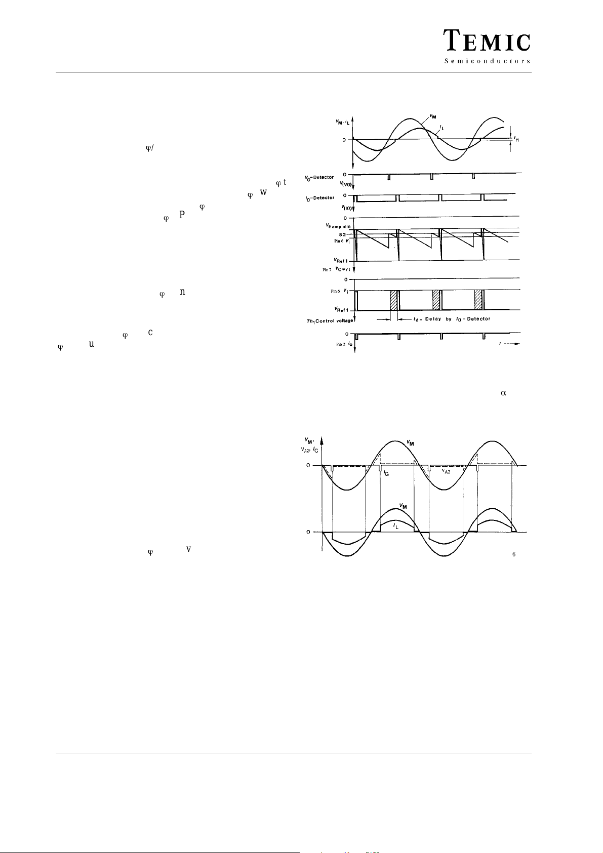
Figure 2. Functional diagram for inductive load of
a
max
In the following zero transition of the mains voltage, the
zero transition detector (Input Pin 5) resets the RS
flip-flop, discharges C
again via S2, and also insures
/t
ö
that the clock flip-flop is in the reset condition. A further
part of the basic function is the current detector with its
input at Pin 4. When controlling inductive loads, the load
current lags behind the mains voltage which means that
the circuit could generate an ignition pulse during the
period in which current is still flowing with a polarity
opposite to that of the mains voltage if the current were
not taken into account (see figure 2).
This, in turn, would lead, to so-called “gaps” in the load
current as the next ignition pulse is generated in the subsequent half-cycle.
2 (8)
Figure 3. Triac voltages + currents at resistive load
V
= Zero cross voltage
o
= Zero cross current
I
O
= Mains voltage
V
M
= Load current
I
L
= Gate current
I
G
V
= Triac voltage at anode HI
HI
TELEFUNKEN Semiconductors
Rev . A1, 28-May-96
95 11360
Page 3
TEA1007
In indication as to whether load current is flowing or not
is provided by the triac itself. When the triac is ignited,
the voltage at electrode H
drops from the instantaneous
1
value of the mains voltage to approximately 1.5 V, the
value of the forward voltage of the triac. When the load
current drops below the hold current of the triac towards
the end of the half-cycle, V
again returns to the instan-
H1
taneous value of the mains voltage. The current detector
with its input at Pin 4 now controls this triac voltage and
blocks the pulse generator via G
and S1by increasing the
1
reference voltage as long as the triac is conducting. As, in
the case of a resistive load, the triac may be extinguished
shortly before the zero transition of the mains voltage –
when the load current drops below the hold current – the
RS flip-flop must prevent any possible second ignition
pulse from being generated.
Additional Function
An internal supply voltage control circuit insures that
output pulses can be generated only when the supply
voltage required for operation of all logic functions is
available.
Series resistance R
+
R
1max
I
= IS + IP + Ix whereas
tot
I
= Total current consumption
tot
I
= Current requirement of the lC
S
I
= A verage current requirement of the triggering pulses
P
I
= Current requirement of other peripheral components
x
can be calculated approx. as follows:
1
V
–V
0.85
Mmin
2 I
Smax
tot
Determination of Gate Series
Resistance, Firing Current and Pulse
Width
95 11359
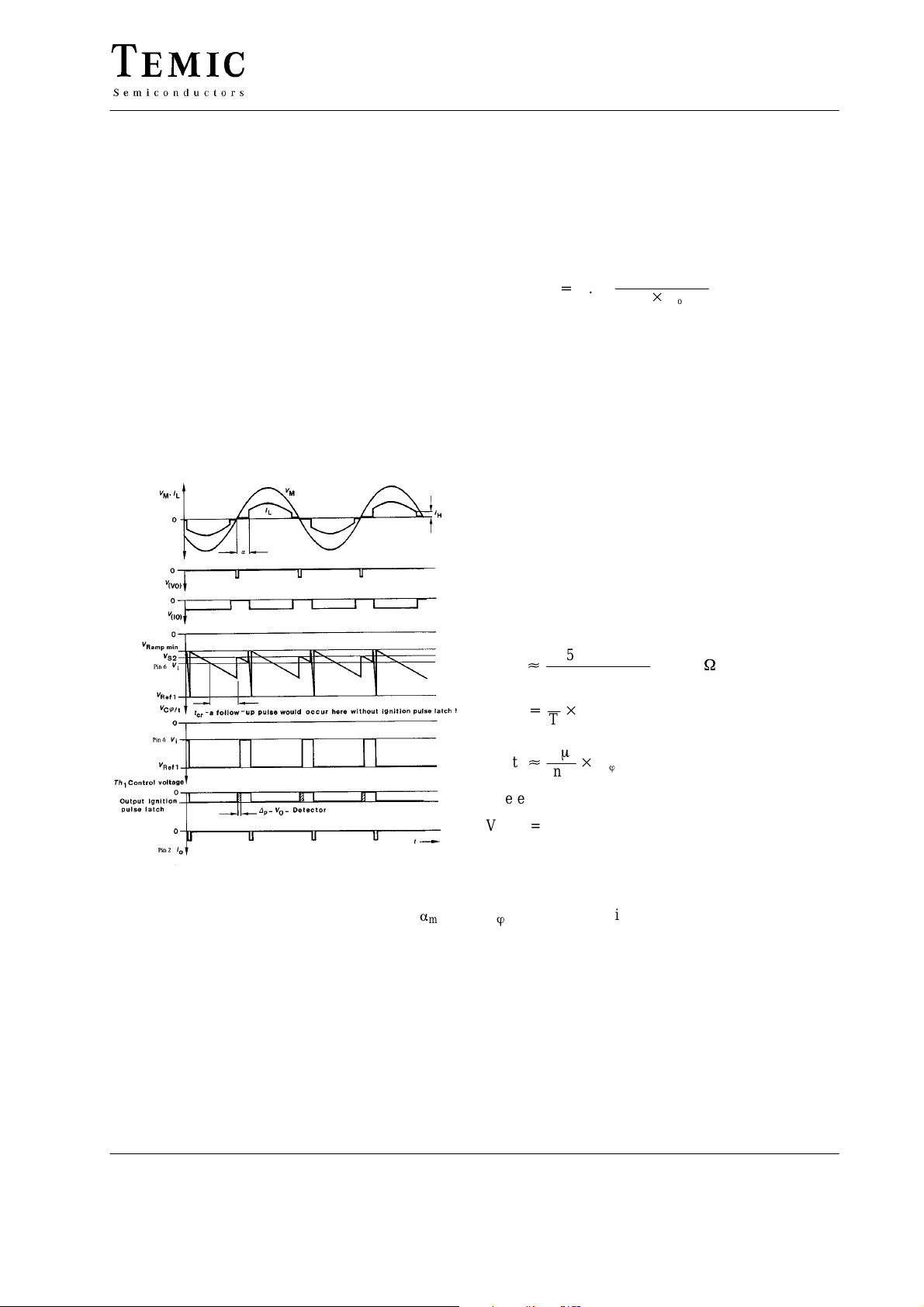
Figure 4. Functional diagram for resistive load and
Firing current requirement depends upon the triac used
which can be regulated with series resistance as given
below:
R
Gmax
[
+
I
P
tP[
12.5 V – V
I
G
T
8ms
nF
I
t
Gmax
p
C
Gmax
– 110
W
ö
whereas:
V
=Triac’s gate voltage
G
=Triac’s gate current
I
G
=Gate current requirement – average
I
P
T =Period duration of mains frequency
=(firing) pulse width
t
p
=Ramp capacitor
a
min
C
ö
TELEFUNKEN Semiconductors
Rev . A1, 28-May-96
3 (8)
Page 4
TEA1007
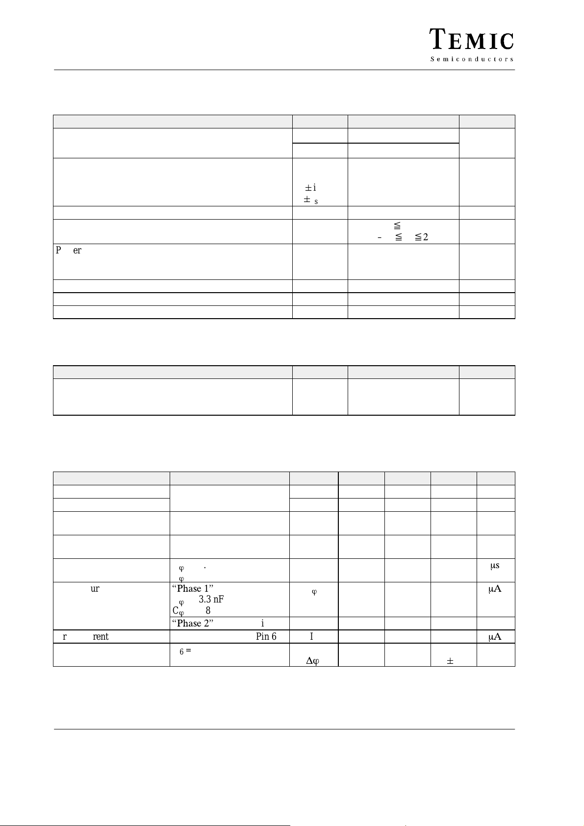
Absolute Maximum Ratings
Reference point Pin 8
Parameters Symbol Value Unit
Current consumption Pin 1 –I
t<10 ms
Sync. currents: Pin 4
Pin 5
t<10 ms Pin 4
Pin 5
Input current Pin 3 –I
Input voltages: Pin 6
Pin 2
Power dissipation
=45°C
T
amb
= 85°C
T
amb
Junction temperature T
Ambient temperature range T
Storage temperature range T
I
"
"
–i
I
syncI
syncV
i
sync.I
i
sync.V
–V
V
P
tot
amb
stg
S
s
30 mA
60
10
mA
10
60
60
I
I
I
5 mA
x
V
–VSx
S
VIx
2
400
V
mW
225
j
125 °C
0 to 80 °C
–40 to +125 °C
Thermal Resistance
Parameters Symbol Value Unit
Junction ambient DIP8
SO8 (P.C.)
SO8 (ceramic)
Electrical Characteristics
Reference point Pin 8, unless otherwise specified
Parameters Test Conditions / Pin Symbol Min Type Max Unit
Mains supply Pin 1 –V
Current consumption I
Sync. currents Pin 4
Pin 5
Output pulse current VS= 13.5 V,
R
= 0, VG = 1.2 V Pin 2 I
G
Output pulse width C
Charge current
= 3.3 nF Pin 2
/t
ö
C
= 6.8 nF
/t
ö
Phase 1"
C
= 3.3 nF
/t
ö
C
= 6.8 nF
/t
ö
Phase 2"
Pin 7
Pin 7 I
Drive current Pin 6 I
Balance between two half
V
= constant
6
cycles
I
I
R
thJA
S
S
syncI.
syncV
t
p
t
p
I
ö
t
i
Dö
200
K/W
220
140
13.5 17 V
2.5 mA
0.35
mA
0.65
mA
O
8
15
1
90 180
30
64
20
m
mA
2
4.3
1.3 mA
0.5
"
3 °
mA
s
4 (8)
TELEFUNKEN Semiconductors
Rev . A1, 28-May-96
Page 5
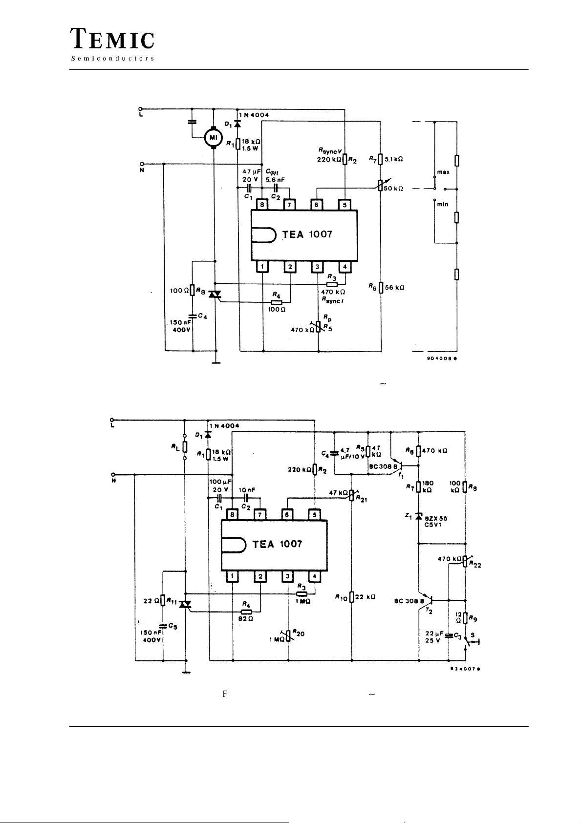
Applications
TEA1007
Figure 5. Phase control for fan motors – 230 V
X
TELEFUNKEN Semiconductors
Rev . A1, 28-May-96
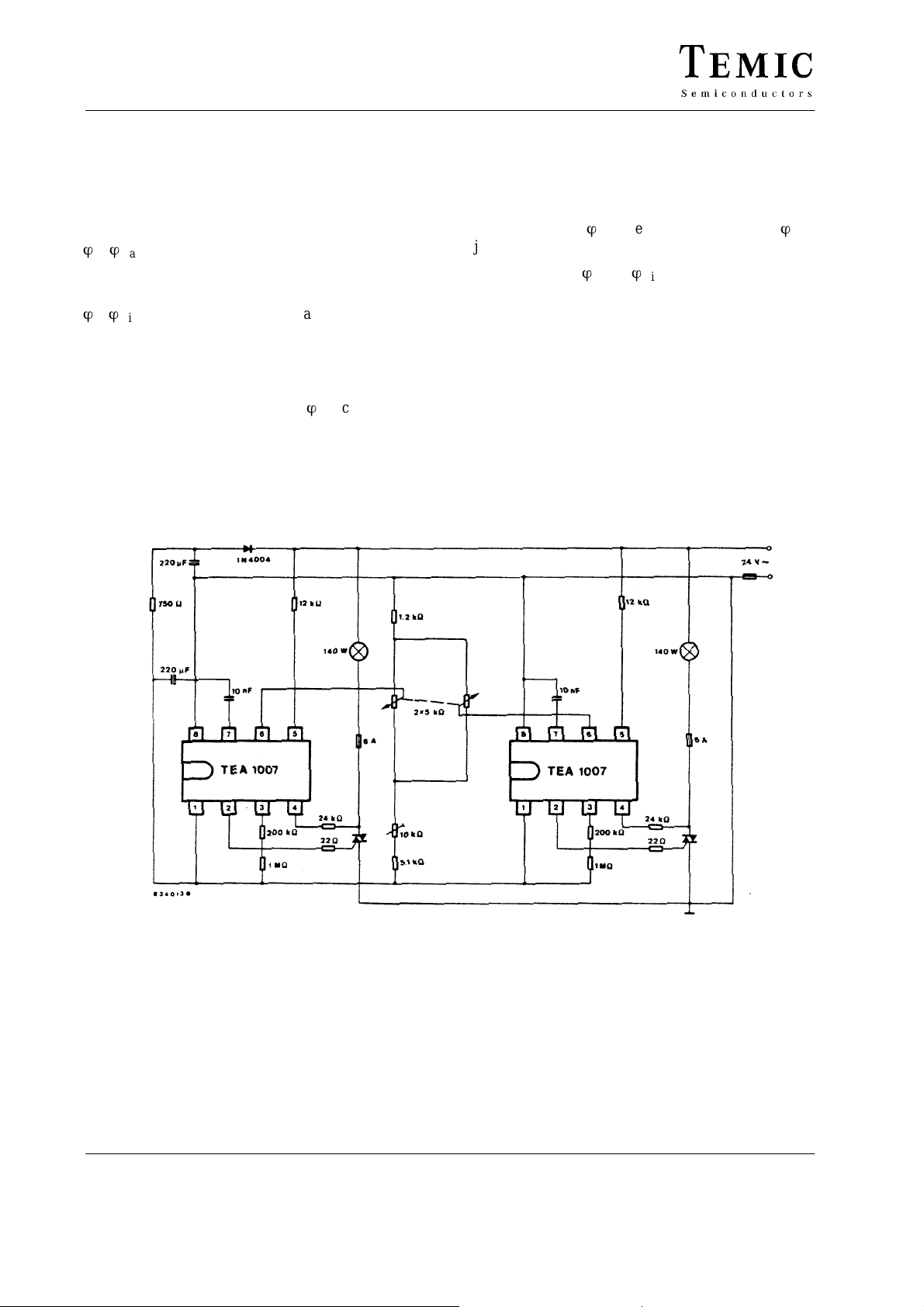
Figure 6. Two-phase time-switch, 230 V
X
5 (8)
Page 6
TEA1007
The timing switch using the TEA 1007 permits two-phase
operation of loads with conduction angle ö adjustable as
required (see figure 6).
Phase 1:
ö
=
ö
max
Period t = 5 to 320 sec adjustable with R
adjustable with R
21
22
Phase 2:
=
ö
ö
min
adjustable with R
20
Period t = optional, or up to the pressed time of switch S
Phase 1 begins as soon as the mains voltage is applied.
The maximum angle of conduction
by means of R
. The timing circuit comprises T1, T2, Z1,
21
can be adjusted
ö
max
C
and R22. As the voltage to which C3is charged
3
increases, the current through Z
potential at the emitter of T
current through Z
1
2
becomes zero, T1can no longer
conduct. The potential on R
conduction angle ö decreases to the value
max
(Phase 2).
20
to
ö
adjustable by means of R
The transition from
ö
following the adjustment of R
decreases. When the
1
has climbed so high that the
therefore drops. The
21
takes place continuously
min
and takes ca. 2 to 20 secs.
22
ö
min
The time constant of Phase 1, which is also determined by
, begins with the release of key S. If S is pressed again
R
22
before the end of the time constant, a period equal to the
complete time-constant is added to the time already run.
The circuit is powered direct from mains via D
every negative half-cycle. C
smooths the operating
1
and R1in
1
voltage which settles at a level of ca. 15.5 V.
,
6 (8)
Figure 7. Fading circuit for manual operation
TELEFUNKEN Semiconductors
Rev . A1, 28-May-96
Page 7
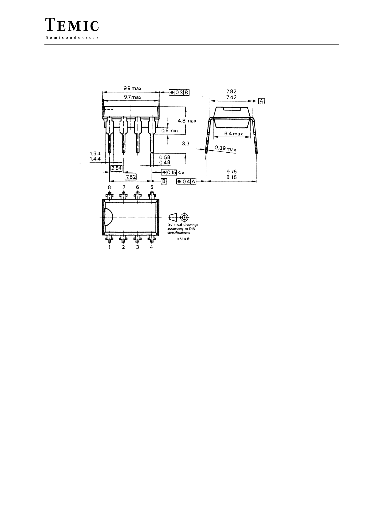
Dimensions in mm
Package: DIP8
TEA1007
TELEFUNKEN Semiconductors
Rev . A1, 28-May-96
7 (8)
Page 8

TEA1007
Ozone Depleting Substances Policy Statement
It is the policy of TEMIC TELEFUNKEN microelectronic GmbH to
1. Meet all present and future national and international statutory requirements.
2. Regularly and continuously improve the performance of our products, processes, distribution and operating systems
with respect to their impact on the health and safety of our employees and the public, as well as their impact on
the environment.
It is particular concern to control or eliminate releases of those substances into the atmosphere which are known as
ozone depleting substances (ODSs).
The Montreal Protocol ( 1987) and its London Amendments (1990) intend to severely restrict the use of ODSs and
forbid their use within the next ten years. Various national and international initiatives are pressing for an earlier ban
on these substances.
TEMIC TELEFUNKEN microelectronic GmbH semiconductor division has been able to use its policy of
continuous improvements to eliminate the use of ODSs listed in the following documents.
1. Annex A, B and list of transitional substances of the Montreal Protocol and the London Amendments respectively
2. Class I and II ozone depleting substances in the Clean Air Act Amendments of 1990 by the Environmental
Protection Agency (EPA) in the USA
3. Council Decision 88/540/EEC and 91/690/EEC Annex A, B and C (transitional substances) respectively.
TEMIC can certify that our semiconductors are not manufactured with ozone depleting substances and do not contain
such substances.
We reserve the right to make changes to improve technical design and may do so without further notice.
Parameters can vary in different applications. All operating parameters must be validated for each customer
application by the customer. Should the buyer use TEMIC products for any unintended or unauthorized
application, the buyer shall indemnify TEMIC against all claims, costs, damages, and expenses, arising out of,
directly or indirectly, any claim of personal damage, injury or death associated with such unintended or
unauthorized use.
8 (8)
TEMIC TELEFUNKEN microelectronic GmbH, P.O.B. 3535, D-74025 Heilbronn, Germany
Telephone: 49 (0)7131 67 2831, Fax number: 49 (0)7131 67 2423
TELEFUNKEN Semiconductors
Rev . A1, 28-May-96
 Loading...