

Page 1

DATA SH EET
Objective specification
File under Integrated Circuits, IC03
1996 Feb 26
INTEGRATED CIRCUITS
TEA1104; TEA1104T
Cost effective battery monitor and
fast charge IC for NiCd and NiMH
chargers
Page 2

1996 Feb 26 2
Philips Semiconductors Objective specification
Cost effective battery monitor and fast
charge IC for NiCd and NiMH chargers
TEA1104; TEA1104T
FEATURES
• Accurate detection of fully charged batteries by
currentless peak voltage sensing
• Switch-over from fast to safe trickle charge current at
battery full detection
• Fast charge termination back-up by maximum time and
maximum temperature detection
• Several trickle charge drive possibilities for mains
isolated and non-mains isolated systems
• Battery checking to protect against short-circuited and
open batteries
• Battery monitor allows recharging of different battery
packs in the same charger
• Dual LED indicator provision
• External regulator not required because of large input
voltage range
• Few low cost external components required.
APPLICATIONS
• Portable telephone
• Portable computer
• Portable audio
• Portable video.
GENERAL DESCRIPTION
The TEA1104 is manufactured in a BiCMOS process
intended to be used as a battery monitor circuit in charge
systems for NiCd and NiMH batteries. It is especially
designed for cost effective compact consumer
applications.
The circuit is able to detect fully charged batteries by
currentless battery voltage sensing. Several output drive
functions are available to control the (reduced) trickle
charge current to keep the batteries full with maximum life
expectations.
The battery full detection is backed up by two independent
mechanisms to make the system fail safe; maximum time
and maximum temperature.
QUICK REFERENCE DATA
ORDERING INFORMATION
SYMBOL PARAMETER CONDITIONS MIN. TYP. MAX. UNIT
V
P
supply voltage 5.45 − 11.5 V
I
P
supply current outputs off −−3mA
V
bat
voltage range of battery full detection 0.81 − 3.6 V
∆V
bat/Vbat
voltage peak detection level with
respect to top value
− 0.25 − %
I
bat
battery monitor input current −−1nA
V
bat(l)
battery voltage protection low − 0.81 0.91 V
V
bat(h)
battery voltage protection high 3.5 3.6 − V
f
osc
oscillator frequency 10 − 100 kHz
TYPE
NUMBER
PACKAGE
NAME DESCRIPTION VERSION
TEA1104 DIP8 plastic dual in-line package; 8 leads (300 mil) SOT97-1
TEA1104T SO8 plastic small outline package; 8 leads; body width 3.9 mm SOT96-1
Page 3
1996 Feb 26 3
Philips Semiconductors Objective specification
Cost effective battery monitor and fast
charge IC for NiCd and NiMH chargers
TEA1104; TEA1104T
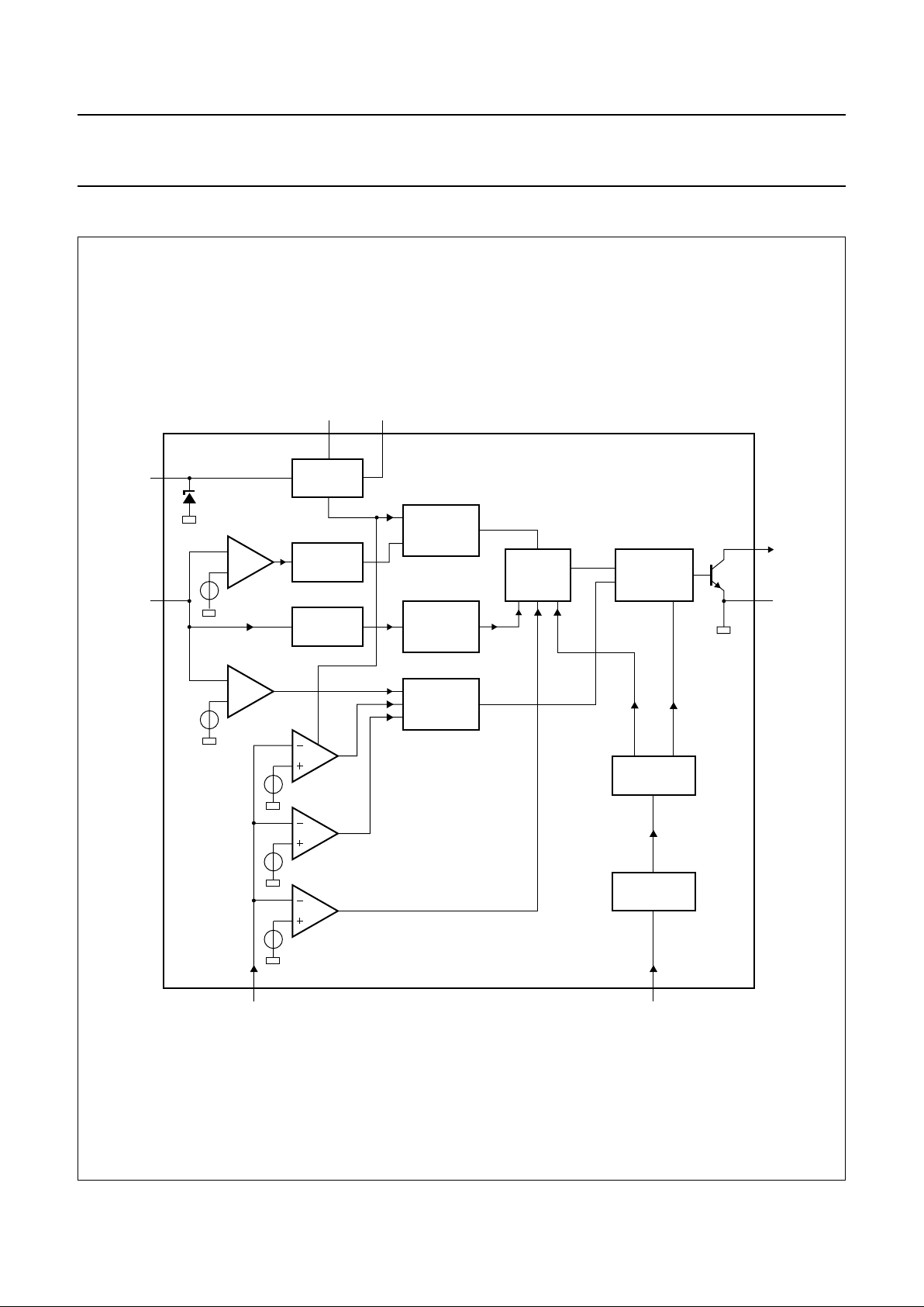
BLOCK DIAGRAM
handbook, full pagewidth
MGE354
SAMPLE-
AND-HOLD
FILTER
BATTERY
FULL
DETECTOR
OR
OR
SUPPLY
MODE
LATCH
OSCILLATOR
TIMER
fast
trickle
CONTROL
battery high
protection
battery low
protection
T
max
T
min
T
cut-off
trickle
TO
4
6
2
7
1
8
5
3
R
ref
V
S
V
P
V
bat
NTC OSC
LED
GND
POR
TEA1104
TEA1104T
Fig.1 Block diagram.
Page 4
1996 Feb 26 4
Philips Semiconductors Objective specification
Cost effective battery monitor and fast
charge IC for NiCd and NiMH chargers
TEA1104; TEA1104T
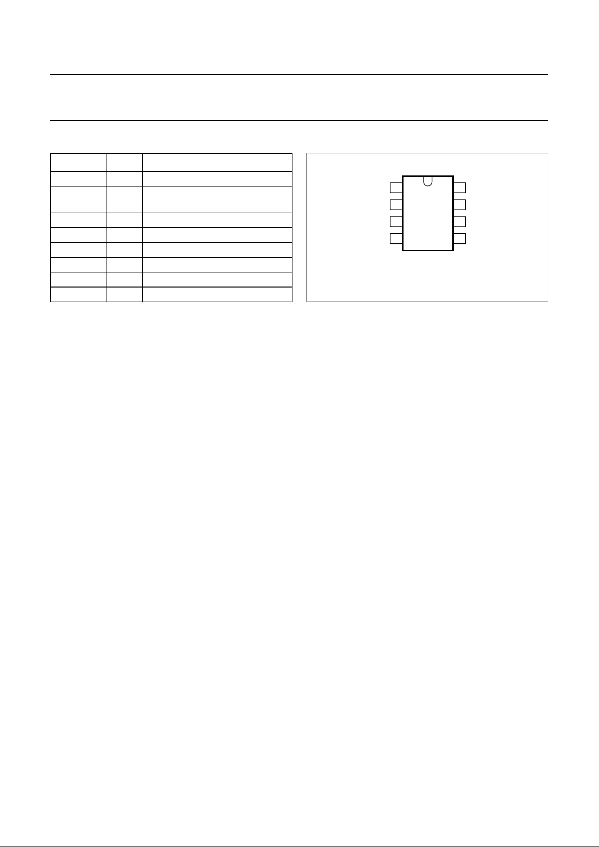
PINNING
SYMBOL PIN DESCRIPTION
GND 1 ground
NTC 2 negative temperature coefficient
resistor input
V
S
3 stabilized supply voltage
V
bat
4 battery voltage sensing
R
ref
5 reference resistor
V
P
6 positive supply voltage
OSC 7 oscillator input
LED 8 LED output
Fig.2 Pin configuration.
handbook, halfpage
1
2
3
4
8
7
6
5
MGE353
TEA1104
LED
OSCNTC
V
P
R
ref
V
bat
V
s
GND
INTRODUCTION
The operation of the TEA1104; TEA1104T is explained
with the aid of the application diagram illustrated in Fig.7.
An application note (AN95085) is available describing the
versatility of the TEA1104; TEA1104T.
An external power current source charges the batteries via
an electronic switch which is controlled by the TEA1104.
The TEA1104 monitors the battery voltage. Fully charged
batteries are detected when the battery voltage peaks. In
fact, a voltage drop of 0.25% with respect to the top value
is detected. Fast charging is initiated at ‘power on’ or at
‘replaced batteries’. The switch is continuously on,
providing that all protection levels are met. At battery full
detection, the charge current is duty cycled to reduce the
average charge current to a lower level, keeping the
batteries fully charged but at he same time assuring long
battery life. In Fig.3 the battery voltage during fast charge
is plotted.
FUNCTIONAL DESCRIPTION
A block diagram of the TEA1104; TEA1104T is illustrated
in Fig.1
Mode latch
The Mode latch determines if the system is in the fast or in
the slow charge mode.
• Fast charge is active at:
– power switch-on and battery connected
– temperature between minimum and maximum value
– battery insert
• Trickle charge is active if:
– battery full is detected
– maximum time is exceeded
– maximum cut-off temperature is exceeded after the
initial phase.
Supply block
For correct start-up, the IC supply current is limited to
35 µA (typ.) until the start-up voltage of 6.4 V is reached
(standby mode). Thereafter, the operating supply voltage
V
P
has to be within the window of 5.45 to 11.5 V, meaning
that there is no need for an external voltage regulator to
supply the IC.
The supply block delivers the following outputs:
• With the help of an external resistor (pin R
ref
), a
reference current is obtained which defines the
accuracy of all IC timing characteristics
• Externally available 4.25 V stabilized voltage source
(V
source
). This source is used internally to supply a large
part of the circuit and can be used to set the NTC biasing
and to supply other external circuitry with a maximum
current of 1 mA. Protection information is provided via
VS, to design a dual LED indicator
• Power-on reset pulse resets all digital circuitry after a
start or restart, due to an interrupted VS.
Page 5

1996 Feb 26 5
Philips Semiconductors Objective specification
Cost effective battery monitor and fast
charge IC for NiCd and NiMH chargers
TEA1104; TEA1104T
Open battery protection
When the rechargeable battery is removed, the output
voltage V
bat
will rise to a high level. The ‘open battery
protection’ block will detect this voltage and the charge
current will be switched off. A digital filter prevents false
open battery protection. The open battery signal
(V
bat
> 3.6 V) must be present for a duration of at least
4 clock pulses.
Battery monitor
One or two cell packs can be connected directly to V
bat
(battery connection) without an external resistor divider. At
larger cell packs the battery voltage must be scaled down
to a voltage range of 0.81 to 3.6 V. It is also possible to
take a tap on the chain of batteries. Battery full is
recognized by voltage peak detection (V
peak
), meaning a
decrease of 0.25% (typ.) with respect to the top value.
Keeping in mind a battery voltage range of 0.81 to 3.6 V
and an accuracy of 10% at V
bat
= 2.4 V for battery full
detection, means that the internal ADC has to be 13 bits.
Several filters are included to prevent false full detection.
The series resistance of the battery and battery connection
can cause battery voltage fluctuations and therefore it is
necessary to stop the charging before sensing; this is
called the ‘inhibit time’. This will be performed
automatically via the regulation output pin LED. The
charging is stopped for ten oscillator periods at the end of
which sampling is performed. The battery voltage will now
be sensed in a currentless way.
Timer/oscillator
The oscillator has a sawtooth shape.
The period time is defined by: t
osc
=K×R
ref
× C
osc
The oscillator frequency is used in the timer block. In this
block several important signals are created.
• Time-out for protecting the fast charge process in time.
Time-out is normally chosen to be 25% longer than the
associated fast charge time. So for a one hour charge
time, time-out = 1.25 hours. The relationship with the
oscillator period time is:
– Time-out = 2 exp28 × t
osc
• The duty factor in the trickle charge mode: The duty
factor is fixed to1⁄40, meaning that the average:
–I
trickle
=1⁄40× I
fast
–ton=3⁄4× 2 exp9 × t
osc
–t
off
= 2 exp14 × t
osc
.
• The battery voltage is sensed each ‘cycle time’. The
cycle time is defined as:
–T
cycle
= 2 exp16 × t
osc
• The ‘inhibit time’ is the time that the charger current is
disabled, after which the battery voltage is sensed in a
currentless way.
–t
inhibit
=10×t
osc
Battery sampling takes one oscillator period for each
cycle interval.
–t
sample=tosc
• The ‘disable time’ is present to correct start-up with flat
or polarized batteries. During the disable time, the
battery full detection is not active.
–t
disable
= 2 exp −5 × time-out
The timer is reset by battery full detection, but is on hold
during the temperature and battery-low protection modes.
Temperature protection block
Temperature sensing is achieved by using a cheap
thermistor. Two temperature windows are built in:
• If the temperature at power-on reset is above the
maximum temperature protection level, the trickle
charge current is active. The same applies for
temperatures below the minimum temperature. Fast
charging starts when the temperature is in between the
minimum and the maximum temperature levels.
• If the temperature is between the maximum and
minimum temperature at power-on reset, the fast charge
current level is active. If the temperature sinks below the
minimum temperature level, again the trickle charge
level is active. At rising temperature, the fast charge
current is latched off at the ‘cut off’ temperature level.
To avoid switching on and off with temperature, a
hysteresis is built in for low temperature level. If the
temperature protection is not necessary, pin ‘Negative
Temperature Coefficient resistor’ (NTC) must be
connected to pin R
ref
.
Battery low protections
When the battery voltage is less than 0.81 V, the circuit
assumes that there are short circuited batteries and the
charge current is reduced to the trickle charge level. If the
batteries are flat, the trickle charge current is able to raise
the battery voltage within an acceptable period of time,
after which fast charging starts.
Page 6

1996 Feb 26 6
Philips Semiconductors Objective specification
Cost effective battery monitor and fast
charge IC for NiCd and NiMH chargers
TEA1104; TEA1104T
Output drivers
Several output drive possibilities are supported by the
TEA1104, to limit the fast charge current and to indicate
the mode that the charge is in.
In mains isolated systems, output drive current is available
for a bipolar or MOS switching device. Moreover, current
regulators can be driven (see Fig.4).
In non mains isolated systems, the current source can be
switched via the auxiliary winding (see Fig.6) using the
TEA140X power plugs.
In the application section, an example is shown driving two
LEDs that are indicating fast charging, protection during
fast charging, full status and removed batteries. It is also
possible to output the same information via one LED only.
Fig.3 NiCd battery characteristics during a 1.25C charge cycle.
handbook, full pagewidth
MGE355
fast charge (I
fast
) trickle charge (I
fast
/40)
t
full
detection
V
bat
I
charge
Fig.4 Output drivers.
handbook, full pagewidth
MGE356
TEA1104
output output
output
LED
TEA1104
LED
TEA1104
LED
LM317
Page 7

1996 Feb 26 7
Philips Semiconductors Objective specification
Cost effective battery monitor and fast
charge IC for NiCd and NiMH chargers
TEA1104; TEA1104T
handbook, full pagewidth
MGE359
Vs > 11.5 V
6.2 V < Vs < 11.5 V
Vs < 5.25 V
no no
yes
yes
yes
yes
yes
no
TIME OUT > 111 min
(TO)
T
bat
≥ 55
o
C
(TCO)
-∆V
bat
≥ 0.25%
and
t
dis
> 3% TO
FAST charge
set T
cut-off
(e.g. 55
o
C)
dual LED
indication
(note 2)
dual LED
indication
dual LED
indication
trickle charge
I
fast
/ 40
battery is FULL
trickle charge
I
fast
/ 40
(note 4)
V
bat
< 0.81 V
or T
bat
< T
min
or T
bat
> T
max
(note 1)
0.81 V < V
bat
< 3.6 V
and
T
min
< T
bat
< T
max
(note 5)
circuit non-active
IDD ≤ 45 µA
total reset logic
set TIME OUT (e.g. 111 min)
set T
max
(e.g. 48
o
C)
T
min
(e.g. 20
o
C)
circuit active
clamp at 11.5 V
I
DDmax
= 25 mA
circuit active
blinks
FAST
blinks
FAST
ON
FAST
blinks
FASTFULL
OFF
ON
FASTFULL
OFF
OFF
FASTFULL
ON
START
no
yes
yes
yes
yes
no
no
no
no
no
no
dual LED
indication
yes
yes
stop charge
total reset
open battery
OFF
FAST
OFF
FASTFULL
OFF
yes
no
(note 3)
Fig.5 Flow chart of the TEA1104.
(1) V
bat
< 0.81V due to empty or flat battery.
(2) For single LED application see Fig.7, for dual LED
application see Fig.6.
(3) V
bat
> 3.6 V due to system occurrence or an external
inhibit via pin V
bat
.
(4) Release via reset.
(5) T
min=VNTC
≥ 2 V; Tmax = V
NTC
≤ 1V;
T
cut-off=VNTC
≤ 0.81 V.
Page 8

1996 Feb 26 8
Philips Semiconductors Objective specification
Cost effective battery monitor and fast
charge IC for NiCd and NiMH chargers
TEA1104; TEA1104T
LIMITING VALUES
In accordance with the Absolute Maximum Rating System (IEC 134); note 1.
Note
1. All voltages are measured with respect to ground; positive currents flow into the IC. The voltage ratings are valid
provided that other ratings are not violated; current ratings are valid provided that the power rating is not violated.
QUALITY SPECIFICATION
In accordance with
“SNW-FQ-611 part E”
. The numbers of the quality specification can be found in the
“Quality
Reference Handbook”
. The handbook can be ordered using the code 9397 750 00192.
SYMBOL PARAMETER CONDITIONS MIN. MAX. UNIT
V
P
supply voltage −0.5 +13.2 V
V
oLED
LED output voltage (pin 8) −0.5 V
P
V
V
iNTC
negative temperature coefficient resistor
input voltage (pin 2)
−0.5 +5 V
V
i(OSC)
oscillator input voltage (pin 7) −0.5 +5 V
V
i(bat)
battery input voltage (pin 4) −0.5 +5 V
V
Rref
reference resistor voltage (pin 5) −0.5 +5 V
I
source
output source current −3 +0.01 mA
I
oLED
LED output current − 25 mA
I
Rref
reference resistor current −1 +0.01 mA
I
bat
battery current −1+1mA
V
P
supply current − 25 mA
P
tot
total power dissipation T
amb
=70°C
TEA1104 − 0.5 W
TEA1104T − 0.35 W
T
amb
operating ambient temperature −20 +70 °C
T
j(max)
maximum operating junction temperature − +150 °C
T
stg
storage temperature −55 +150 °C
Page 9

1996 Feb 26 9
Philips Semiconductors Objective specification
Cost effective battery monitor and fast
charge IC for NiCd and NiMH chargers
TEA1104; TEA1104T
CHARACTERISTICS
V
P
= 10 V; T
amb
=25°C; R
ref
=33kΩ;C
OSC
= 1 nF; unless otherwise specified.
SYMBOL PARAMETER CONDITIONS MIN. TYP. MAX. UNIT
Supply
V
P
supply voltage 5.45 − 11.5 V
∆V
P
/∆t supply voltage start rate −− 0.5 V/µs
V
clamp
clamping voltage I
clamp
=25mA 11.5 − 12.8 V
V
start
start-up voltage 6.1 6.4 6.7 V
V
pd
power-down voltage level 4.65 5.05 5.45 V
I
P
supply current outputs off −− 3mA
I
start
start-up current VP=4V − 45 50 µA
V
S
stabilized voltage IS= 1 mA 4.03 4.25 4.46 V
V
Rref
voltage range at reference resistor I
Rref
=20µA 1.18 1.25 1.31 V
TC
Vref
temperature coefficient of the
reference voltage
T
amb
= 0 to 45 °C −±60 ±120 ppm/K
I
Rref
current range of the reference
resistor
10 − 100 µA
Temperature related input; NTC
V
i(co)
input voltage level for detecting
temperature cut-off
0.75 0.81 0.87 V
V
i(co; max)
maximum input voltage level for
detecting temperature cut-off
0.92 1.0 1.08 V
V
i(co; min)
minimum input voltage level for
detecting temperature cut-off
1.85 2.0 2.15 V
I
NTC
input current V
NTC
= 1.5 V −5 − +5 µA
Output drivers
δ
LED
LED pulse duty factor 2.4 2.5 2.6 %
V
LED(sat)
LED saturation voltage I
LED(sat)
=15mA −− 600 mV
I
LI(LED)
LED input leakage current V
LED
=15V −− 5 µA
Battery monitor
I
i(bat)
input battery current V
bat
= 2.4 V − 1 − nA
V
bat
voltage range for peak detection 0.81 − 3.6 V
∆V
bat/Vbat
peak detection level with respect to
top level
V
bat
=2V − 0.25 − %
T
j
temperature range of peak
detection
0 − 50 °C
Protections; BAT
V
bat(l)
low level battery protection voltage − 0.81 0.91 V
V
bat(h)
high level battery protection voltage 3.5 3.6 4.5 V
Oscillator
k correction factor 0.84 0.93 1.02
f
osc
frequency range 10 − 100 kHz
Page 10

1996 Feb 26 10
Philips Semiconductors Objective specification
Cost effective battery monitor and fast
charge IC for NiCd and NiMH chargers
TEA1104; TEA1104T
APPLICATION INFORMATION
A guideline for the settings of TEA1104 and its external
components selection is given based on an example of a
1 hour charger for a 4 cell NiCd or NiMH battery pack. The
basic application diagram as illustrated in Fig.6 which is
based on the application diagram illustrated in Fig.7 with
some additional components; a 2 LED charge status
indication has been provided.
For charging a battery within one hour the charge current
rating should be as follows:
Required minimum charge current = battery
capacity × 1.2/charge time.
Therefore, for a 1 Ah battery the external charge current
supply has to deliver at least 1.2 A.
TEA1104 settings
The fast charge back-up timer period, time-out, has to be
set in relation to the expected maximum charge time.
Normally, a safety back-up time is chosen approximately
25% longer than the maximum expected fast charge time.
For a one hour charger the time-out period can be set to
1.25 h.
Time-out relationship with the oscillator repetition time is
as follows;
t
osc
= time-out (h) × 3600/2 exp28
t
osc
=17µs for time-out = 1.25 h
t
osc
is set with the combination of C
osc
and R
ref
;
where t
osc
= 0.93 × R
ref
× C
osc
.
R
ref
can be chosen between 13 and 120 kΩ, but a 27 kΩ
resistor is recommended. The oscillator capacitor can be
calculated which is 668 pF; the nearest higher practical
value is 680 pF.
In the trickle charge mode the LED output will pulsate with
a repetition time; t
trickle
= 2 exp14 × t
osc
= 0.28 s.
The duty factor of the pulse is 2.5% of t
trickle
. This duty
factor also applies to the charge current as the charge
current switch is driven by the LED output. Therefore, the
average trickle charge current is I
fast
/40. The V
bat
input
can be adapted to the battery voltage via the resistor
dividers R1 and R2. When an NTC thermistor has been
incorporated into the battery, the minimum, maximum and
cut-off temperature levels can be set with the resistors R3
and R4. For an NTC with a common sensitivity of 3965
and adjustment resistor values R3 = 13 kΩ, R4 = 20 kΩ
the minimum, maximum and cut-off temperatures will be 5,
42 and 50 °C respectively.
The flow chart of the TEA1104; TEA1104A is given in
Fig.5. The load state of the batteries can be displayed by
one or two LEDs. The flow chart is not to be regarded as
sequential. Each mode of operation is a purely separate
continuous process.
Table 1 Dual LED indication
CHARGER
MODE
V
LED
V
S
LED 1 LED 2
Fast charging low high on off
Fast charging
protection
low/high high on/off off
Full
(trickle charging)
low/high low off on
Battery open high high off off
Page 11

1996 Feb 26 11
Philips Semiconductors Objective specification
Cost effective battery monitor and fast
charge IC for NiCd and NiMH chargers
TEA1104; TEA1104T
Fig.6 Basic application diagram.
handbook, full pagewidth
MGE357
LED V
P
VsV
bat
TEA1104
GND OSCVref NTC
LED1
FAST
BAW62
5.1
kΩ
1.2
kΩ
47
kΩ
100
kΩ
270
Ω
BD434
BC548
BC548
LED 2
FULL
C
osc
R
ref
R4
R3
R2
R1
4
cells
VP = 6.5 to 12 V
−θ
current
supply
+
+
−
+
−
Fig.7 Application diagram.
handbook, full pagewidth
MGE358
TEA1104
684 3
1752
−θ
Page 12

1996 Feb 26 12
Philips Semiconductors Objective specification
Cost effective battery monitor and fast
charge IC for NiCd and NiMH chargers
TEA1104; TEA1104T
PACKAGE OUTLINES
UNIT
A
max.
A
1
A2A
3
b
p
cD
(1)E(2)
(1)
eHELLpQZywv θ
REFERENCES
OUTLINE
VERSION
EUROPEAN
PROJECTION
ISSUE DATE
IEC JEDEC EIAJ
mm
inches
1.75
0.25
0.10
1.45
1.25
0.25
0.49
0.36
0.25
0.19
5.0
4.8
4.0
3.8
1.27
6.2
5.8
1.05
0.7
0.6
0.7
0.3
8
0
o
o
0.25 0.10.25
DIMENSIONS (inch dimensions are derived from the original mm dimensions)
Notes
1. Plastic or metal protrusions of 0.15 mm maximum per side are not included.
2. Plastic or metal protrusions of 0.25 mm maximum per side are not included.
1.0
0.4
SOT96-1
X
w M
θ
A
A
1
A
2
b
p
D
H
E
L
p
Q
detail X
E
Z
e
c
L
v M
A
(A )
3
A
4
5
pin 1 index
1
8
y
076E03S MS-012AA
0.069
0.010
0.004
0.057
0.049
0.01
0.019
0.014
0.0100
0.0075
0.20
0.19
0.16
0.15
0.050
0.244
0.228
0.028
0.024
0.028
0.012
0.010.010.041 0.004
0.039
0.016
0 2.5 5 mm
scale
SO8: plastic small outline package; 8 leads; body width 3.9 mm
SOT96-1
95-02-04
97-05-22
Page 13

1996 Feb 26 13
Philips Semiconductors Objective specification
Cost effective battery monitor and fast
charge IC for NiCd and NiMH chargers
TEA1104; TEA1104T
REFERENCES
OUTLINE
VERSION
EUROPEAN
PROJECTION
ISSUE DATE
IEC JEDEC EIAJ
SOT97-1
92-11-17
95-02-04
UNIT
A
max.
12
b
1
(1) (1)
(1)
b
2
cD E e M
Z
H
L
mm
DIMENSIONS (inch dimensions are derived from the original mm dimensions)
A
min.
A
max.
b
max.
w
M
E
e
1
1.73
1.14
0.53
0.38
0.36
0.23
9.8
9.2
6.48
6.20
3.60
3.05
0.2542.54 7.62
8.25
7.80
10.0
8.3
1.154.2 0.51 3.2
inches
0.068
0.045
0.021
0.015
0.014
0.009
1.07
0.89
0.042
0.035
0.39
0.36
0.26
0.24
0.14
0.12
0.010.10 0.30
0.32
0.31
0.39
0.33
0.0450.17 0.020 0.13
b
2
050G01 MO-001AN
M
H
c
(e )
1
M
E
A
L
seating plane
A
1
w M
b
1
e
D
A
2
Z
8
1
5
4
b
E
0 5 10 mm
scale
Note
1. Plastic or metal protrusions of 0.25 mm maximum per side are not included.
pin 1 index
DIP8: plastic dual in-line package; 8 leads (300 mil)
SOT97-1
Page 14

1996 Feb 26 14
Philips Semiconductors Objective specification
Cost effective battery monitor and fast
charge IC for NiCd and NiMH chargers
TEA1104; TEA1104T
SOLDERING
Introduction
There is no soldering method that is ideal for all IC
packages. Wave soldering is often preferred when
through-hole and surface mounted components are mixed
on one printed-circuit board. However, wave soldering is
not always suitable for surface mounted ICs, or for
printed-circuits with high population densities. In these
situations reflow soldering is often used.
This text gives a very brief insight to a complex technology.
A more in-depth account of soldering ICs can be found in
our
“IC Package Databook”
(order code 9398 652 90011).
DIP
SOLDERING BY DIPPING OR BY WA VE
The maximum permissible temperature of the solder is
260 °C; solder at this temperature must not be in contact
with the joint for more than 5 seconds. The total contact
time of successive solder waves must not exceed
5 seconds.
The device may be mounted up to the seating plane, but
the temperature of the plastic body must not exceed the
specified maximum storage temperature (T
stg max
). If the
printed-circuit board has been pre-heated, forced cooling
may be necessary immediately after soldering to keep the
temperature within the permissible limit.
R
EPAIRING SOLDERED JOINTS
Apply a low voltage soldering iron (less than 24 V) to the
lead(s) of the package, below the seating plane or not
more than 2 mm above it. If the temperature of the
soldering iron bit is less than 300 °C it may remain in
contact for up to 10 seconds. If the bit temperature is
between 300 and 400 °C, contact may be up to 5 seconds.
SO
REFLOW SOLDERING
Reflow soldering techniques are suitable for all SO
packages.
Reflow soldering requires solder paste (a suspension of
fine solder particles, flux and binding agent) to be applied
to the printed-circuit board by screen printing, stencilling or
pressure-syringe dispensing before package placement.
Several techniques exist for reflowing; for example,
thermal conduction by heated belt. Dwell times vary
between 50 and 300 seconds depending on heating
method. Typical reflow temperatures range from
215 to 250 °C.
Preheating is necessary to dry the paste and evaporate
the binding agent. Preheating duration: 45 minutes at
45 °C.
W
AVE SOLDERING
Wave soldering techniques can be used for all SO
packages if the following conditions are observed:
• A double-wave (a turbulent wave with high upward
pressure followed by a smooth laminar wave) soldering
technique should be used.
• The longitudinal axis of the package footprint must be
parallel to the solder flow.
• The package footprint must incorporate solder thieves at
the downstream end.
During placement and before soldering, the package must
be fixed with a droplet of adhesive. The adhesive can be
applied by screen printing, pin transfer or syringe
dispensing. The package can be soldered after the
adhesive is cured.
Maximum permissible solder temperature is 260 °C, and
maximum duration of package immersion in solder is
10 seconds, if cooled to less than 150 °C within
6 seconds. Typical dwell time is 4 seconds at 250 °C.
A mildly-activated flux will eliminate the need for removal
of corrosive residues in most applications.
R
EPAIRING SOLDERED JOINTS
Fix the component by first soldering two diagonallyopposite end leads. Use only a low voltage soldering iron
(less than 24 V) applied to the flat part of the lead. Contact
time must be limited to 10 seconds at up to 300 °C. When
using a dedicated tool, all other leads can be soldered in
one operation within 2 to 5 seconds between
270 and 320 °C.
Page 15

1996 Feb 26 15
Philips Semiconductors Objective specification
Cost effective battery monitor and fast
charge IC for NiCd and NiMH chargers
TEA1104; TEA1104T
DEFINITIONS
LIFE SUPPORT APPLICATIONS
These products are not designed for use in life support appliances, devices, or systems where malfunction of these
products can reasonably be expected to result in personal injury. Philips customers using or selling these products for
use in such applications do so at their own risk and agree to fully indemnify Philips for any damages resulting from such
improper use or sale.
Data sheet status
Objective specification This data sheet contains target or goal specifications for product development.
Preliminary specification This data sheet contains preliminary data; supplementary data may be published later.
Product specification This data sheet contains final product specifications.
Limiting values
Limiting values given are in accordance with the Absolute Maximum Rating System (IEC 134). Stress above one or
more of the limiting values may cause permanent damage to the device. These are stress ratings only and operation
of the device at these or at any other conditions above those given in the Characteristics sections of the specification
is not implied. Exposure to limiting values for extended periods may affect device reliability.
Application information
Where application information is given, it is advisory and does not form part of the specification.
Page 16

Philips Semiconductors – a worldwide company
Argentina: IEROD, Av. Juramento 1992 - 14.b, (1428)
BUENOS AIRES, Tel. (541)786 7633, Fax. (541)786 9367
Australia: 34 Waterloo Road, NORTH RYDE, NSW 2113,
Tel. (02)805 4455, Fax. (02)805 4466
Austria: Triester Str. 64, A-1101 WIEN, P.O. Box 213,
Tel. (01)60 101-1236, Fax. (01)60 101-1211
Belgium: Postbus 90050, 5600 PB EINDHOVEN, The Netherlands,
Tel. (31)40-2783749, Fax. (31)40-2788399
Brazil: Rua do Rocio 220 - 5
th
floor, Suite 51,
CEP: 04552-903-SÃO PAULO-SP, Brazil,
P.O. Box 7383 (01064-970),
Tel. (011)821-2333, Fax. (011)829-1849
Canada: PHILIPS SEMICONDUCTORS/COMPONENTS:
Tel. (800) 234-7381, Fax. (708) 296-8556
Chile: Av. Santa Maria 0760, SANTIAGO,
Tel. (02)773 816, Fax. (02)777 6730
China/Hong Kong: 501 Hong Kong Industrial Technology Centre,
72 Tat Chee Avenue, Kowloon Tong, HONG KONG,
Tel. (852)2319 7888, Fax. (852)2319 7700
Colombia: IPRELENSO LTDA, Carrera 21 No. 56-17,
77621 BOGOTA, Tel. (571)249 7624/(571)217 4609,
Fax. (571)217 4549
Denmark: Prags Boulevard 80, PB 1919, DK-2300
COPENHAGEN S, Tel. (45)32 88 26 36, Fax. (45)31 57 19 49
Finland: Sinikalliontie 3, FIN-02630 ESPOO,
Tel. (358)0-615 800, Fax. (358)0-61580 920
France: 4 Rue du Port-aux-Vins, BP317,
92156 SURESNES Cedex,
Tel. (01)4099 6161, Fax. (01)4099 6427
Germany: P.O. Box 10 51 40, 20035 HAMBURG,
Tel. (040)23 53 60, Fax. (040)23 53 63 00
Greece: No. 15, 25th March Street, GR 17778 TAVROS,
Tel. (01)4894 339/4894 911, Fax. (01)4814 240
India: Philips INDIA Ltd, Shivsagar Estate, A Block,
Dr. Annie Besant Rd. Worli, Bombay 400 018
Tel. (022)4938 541, Fax. (022)4938 722
Indonesia: Philips House, Jalan H.R. Rasuna Said Kav. 3-4,
P.O. Box 4252, JAKARTA 12950,
Tel. (021)5201 122, Fax. (021)5205 189
Ireland: Newstead, Clonskeagh, DUBLIN 14,
Tel. (01)7640 000, Fax. (01)7640 200
Italy: PHILIPS SEMICONDUCTORS S.r.l.,
Piazza IV Novembre 3, 20124 MILANO,
Tel. (0039)2 6752 2531, Fax. (0039)2 6752 2557
Japan: Philips Bldg 13-37, Kohnan 2-chome, Minato-ku, TOKYO 108,
Tel. (03)3740 5130, Fax. (03)3740 5077
Korea: Philips House, 260-199 Itaewon-dong,
Yongsan-ku, SEOUL, Tel. (02)709-1412, Fax. (02)709-1415
Malaysia: No. 76 Jalan Universiti, 46200 PETALING JAYA,
SELANGOR, Tel. (03)750 5214, Fax. (03)757 4880
Mexico: 5900 Gateway East, Suite 200, EL PASO, TX 79905,
Tel. 9-5(800)234-7381, Fax. (708)296-8556
Netherlands: Postbus 90050, 5600 PB EINDHOVEN, Bldg. VB,
Tel. (040)2783749, Fax. (040)2788399
New Zealand: 2 Wagener Place, C.P.O. Box 1041, AUCKLAND,
Tel. (09)849-4160, Fax. (09)849-7811
Norway: Box 1, Manglerud 0612, OSLO,
Tel. (022)74 8000, Fax. (022)74 8341
Pakistan: Philips Electrical Industries of Pakistan Ltd.,
Exchange Bldg. ST-2/A, Block 9, KDA Scheme 5, Clifton,
KARACHI 75600, Tel. (021)587 4641-49,
Fax. (021)577035/5874546
Philippines: PHILIPS SEMICONDUCTORS PHILIPPINES Inc.,
106 Valero St. Salcedo Village, P.O. Box 2108 MCC, MAKATI,
Metro MANILA, Tel. (63) 2 816 6380, Fax. (63) 2 817 3474
Portugal: PHILIPS PORTUGUESA, S.A.,
Rua dr. António Loureiro Borges 5, Arquiparque - Miraflores,
Apartado 300, 2795 LINDA-A-VELHA,
Tel. (01)4163160/4163333, Fax. (01)4163174/4163366
Singapore: Lorong 1, Toa Payoh, SINGAPORE 1231,
Tel. (65)350 2000, Fax. (65)251 6500
South Africa: S.A. PHILIPS Pty Ltd.,
195-215 Main Road Martindale, 2092 JOHANNESBURG,
P.O. Box 7430, Johannesburg 2000,
Tel. (011)470-5911, Fax. (011)470-5494
Spain: Balmes 22, 08007 BARCELONA,
Tel. (03)301 6312, Fax. (03)301 42 43
Sweden: Kottbygatan 7, Akalla. S-164 85 STOCKHOLM,
Tel. (0)8-632 2000, Fax. (0)8-632 2745
Switzerland: Allmendstrasse 140, CH-8027 ZÜRICH,
Tel. (01)488 2211, Fax. (01)481 77 30
Taiwan: PHILIPS TAIWAN Ltd., 23-30F, 66, Chung Hsiao West
Road, Sec. 1. Taipeh, Taiwan ROC, P.O. Box 22978,
TAIPEI 100, Tel. (886) 2 382 4443, Fax. (886) 2 382 4444
Thailand: PHILIPS ELECTRONICS (THAILAND) Ltd.,
209/2 Sanpavuth-Bangna Road Prakanong,
Bangkok 10260, THAILAND,
Tel. (66) 2 745-4090, Fax. (66) 2 398-0793
Turkey:Talatpasa Cad. No. 5, 80640 GÜLTEPE/ISTANBUL,
Tel. (0212)279 27 70, Fax. (0212)282 67 07
Ukraine: Philips UKRAINE, 2A Akademika Koroleva str., Office 165,
252148 KIEV, Tel.380-44-4760297, Fax. 380-44-4766991
United Kingdom: Philips Semiconductors LTD.,
276 Bath Road, Hayes, MIDDLESEX UB3 5BX,
Tel. (0181)730-5000, Fax. (0181)754-8421
United States:811 East Arques Avenue, SUNNYVALE,
CA 94088-3409, Tel. (800)234-7381, Fax. (708)296-8556
Uruguay: Coronel Mora 433, MONTEVIDEO,
Tel. (02)70-4044, Fax. (02)92 0601
Internet: http://www.semiconductors.philips.com/ps/
For all other countries apply to: Philips Semiconductors,
International Marketing and Sales, Building BE-p,
P.O. Box 218, 5600 MD EINDHOVEN, The Netherlands,
Telex 35000 phtcnl, Fax. +31-40-2724825
SCDS47 © Philips Electronics N.V. 1996
All rights are reserved. Reproduction in whole or in part is prohibited without the
prior written consent of the copyright owner.
The information presented in this document does not form part of any quotation
or contract, is believed to be accurate and reliable and may be changed without
notice. No liability will be accepted by the publisher for any consequence of its
use. Publication thereof does not convey nor imply any license under patent- or
other industrial or intellectual property rights.
Printed in The Netherlands
417021/1100/02/pp16 Date of release: 1996 Feb 26
Document order number: 9397 750 00692
 Loading...