

Page 1

INTEGRATED CIRCUITS
DATA SH EET
TEA1098
Speech and handsfree IC
Product specification
Supersedes data of 2000 Sep 26
File under Integrated Circuits, IC03
2001 Aug 24
Page 2

Philips Semiconductors Product specification
Speech and handsfree IC TEA1098
FEATURES
Line interface
• Low DC line voltage
• Voltage regulator with adjustable DC voltage
• Symmetrical high impedance inputs (70 kΩ) for
dynamic, magnetic40 or electret microphones
• DTMF input with confidence tone on earphone and/or
loudspeaker
• Receive amplifier for dynamic, magnetic or
piezo-electric earpieces(with externally adjustable gain)
• Automatic Gain Control (AGC) for true line loss
compensation.
Supplies
• Provides a strong 3.35 V regulated supply for
microcontrollers or diallers
• Provides filtered power supply, optimized according to
line current
• Filtered 2.0 V power supply output for electret
microphone
• PD logic input for power-down.
Handsfree
• Asymmetrical high input impedance for electret
microphone
• Loudspeaker amplifier with single-ended rail-to-rail
output and externally adjustable gain
• Dynamic limiter on loudspeaker amplifier to prevent
distortion
• Logarithmic volume controlon loudspeakeramplifier via
linear potentiometer
• Duplex controller consisting of:
– Signal and noise envelope monitors for both
channels (with adjustable sensitivities and timing)
– Decision logic (with adjustable switch-over and Idle
mode timing)
– Voice switch control (with adjustable switching range
and constant sum of gain during switching).
APPLICATIONS
• Line powered telephone sets.
GENERAL DESCRIPTION
The TEA1098 is an analog bipolar circuit dedicated to
telephonyapplications. It includesa line interface,handset
(HS) microphone and earpiece amplifiers, handsfree (HF)
microphone and loudspeaker amplifiers and a duplex
controller with signal and noise monitors on both channels.
This IC provides a 3.35 V supply for a microcontroller or
dialler and a 2.0 V filtered voltage supply for an electret
microphone.
ORDERING INFORMATION
TYPE
NUMBER
TEA1098TV VSO40 plastic very small outline package; 40 leads SOT158-1
TEA1098UH − bare die; on foil −
2001 Aug 24 2
NAME DESCRIPTION VERSION
PACKAGE
Page 3

Philips Semiconductors Product specification
Speech and handsfree IC TEA1098
QUICK REFERENCE DATA
I
= 15 mA; R
line
connected to pin LN;
specified.
SYMBOL PARAMETER CONDITIONS MIN. TYP. MAX. UNIT
I
line
V
SLPE
V
BB
V
DD
I
BB
I
BB(pd)
G
v(MIC-LN)
G
v(IR-RECO)
∆G
v(QR)
G
v(TXIN-TXOUT)
G
v(HFTX-LN)
G
v(HFRX-LSAO
SWRA switching range − 40 − dB
∆SWRA switching range adjustment R
∆G
v(trx)
SLPE
=20Ω;Z
= 600 Ω; f = 1 kHz;T
line
=25°C forTEA1098TV;Tj=25°C forTEA1098UH; pin AGC
amb
PD = HIGH; HFC = LOW; MUTE = HIGH; measured according to test circuit; unless otherwise
line current operating range normal operation 11 − 130 mA
with reduced performance 1 − 11 mA
stabilized voltage between
pins SLPE and GND
regulated supply voltage for
internal circuitry
regulated supply voltage on
pin V
DD
current available on pin V
BB
I
= 15 mA 3.4 3.7 4.0 V
line
I
= 70 mA 5.7 6.1 6.5 V
line
I
= 15 mA 2.75 3.0 3.25 V
line
I
= 70 mA 4.9 5.3 5.7 V
line
VBB> 3.35 V + 0.25 V (typ.) 3.1 3.35 3.6 V
otherwise − V
− 0.25 − V
BB
in speech mode − 11 − mA
in handsfree mode − 9 − mA
current consumption on V
BB
PD = LOW − 460 −µA
during power-down phase
voltagegain from pins MIC+/MIC−
V
= 5 mV (RMS) 43.3 44.3 45.3 dB
MIC
to LN
voltage gain from pin IR
VIR= 8 mV (RMS) 28.7 29.7 30.7 dB
(referenced to LN) to RECO
gain voltage range between
−3 − +15 dB
pins RECO and QR
voltage gain from pin TXIN to
TXOUT
voltage gain from pin HFTX to LN V
) voltage gain from pinHFRX
to LSAO
gain control range for transmitand
V
= 3 mV (RMS);
TXIN
R
= 30.1 kΩ
GATX
= 15 mV (RMS) 33.5 34.7 35.9 dB
HFTX
V
= 30 mV (RMS);
HFRX
R
= 255 kΩ; I
GALS
= 365 kΩ−40 − +12 dB
SWR
I
= 70 mA 5.45 6.45 7.45 dB
line
=70mA
line
12.7 15.2 17.7 dB
25.5 28 30.5 dB
receive amplifiers affected by the
AGC; with respect to I
=15mA
line
2001 Aug 24 3
Page 4
Philips Semiconductors Product specification
Speech and handsfree IC TEA1098
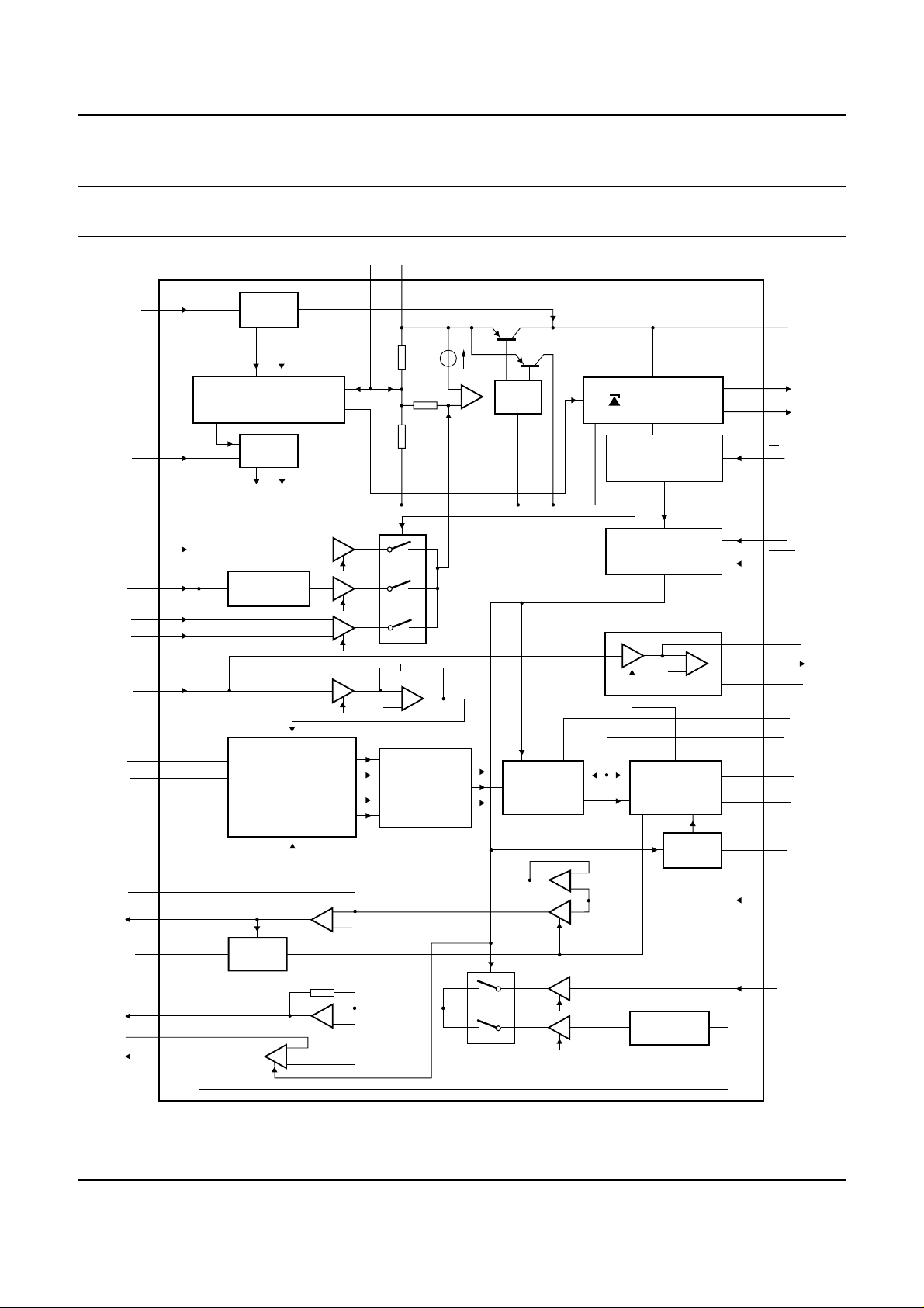
BLOCK DIAGRAM
REG
handbook, full pagewidth
LN 18
STARTER
LINE CURRENT DETECTION
LOW VOLTAGE BEHAVIOUR
19 17
SLPE
R1
SWITCH
SUPPLY
MANAGEMENT
13
V
BB
V
22
DD
MICS
23
AGC
GND
HFTX
DTMF
MIC+
MIC−
TXIN
TSEN
TENV
TNOI
RNOI
RENV
RSEN
GALS
LSAO
30
24
25
40
29
32
27
28
26
1
2
5
PD
HFC
MUTE
GATX
TXOUT
GNDTX
SWT
IDT
STAB
SWR
VOL
HFRX
21
16
39
35
34
33
31
8
7
6
9
11
10
14
15
AGC
Tail currents for preamps
ATTENUATOR
TX AND RX
ENVELOPE AND NOISE
DETECTORS
BUFFERS
AND
COMPARATORS
TEA1098TV
DUCO LOGIC
SWT STATUS
POWER-DOWN
CURRENT SOURCES
LOGIC
INPUTS
DECODING
VOICE
SWITCH
VOLUME
CONTROL
12
DLC
RECO
GARX
QR
38
37
36
DYNAMIC
LIMITER
Fig.1 Block diagram.
2001 Aug 24 4
ATTENUATOR
20
MGL317
IR
Page 5

Philips Semiconductors Product specification
Speech and handsfree IC TEA1098
PINNING
SYMBOL
PD 1 40 power-down input (active LOW)
MUTE 2 41 logic input (active LOW)
n.c. 3 42 not connected
n.c. 4 43 not connected
n.c. − 44 not connected
HFRX 5 1 receive input for loudspeaker amplifier
TNOI 6 2 transmit noise envelope timing adjustment
TENV 7 3 transmit signal envelope timing adjustment
TSEN 8 4 transmit signal envelope sensitivity adjustment
RNOI 9 5 receive noise envelope timing adjustment
RSEN 10 6 receive signal envelope sensitivity adjustment
RENV 11 7 receive signal envelope timing adjustment
DLC 12 8 dynamic limiter capacitor for the loudspeaker amplifier
V
BB
GALS 14 10 loudspeaker amplifier gain adjustment
LSAO 15 11 loudspeaker amplifier output
n.c. − 12 not connected
GND 16 13 ground reference
SLPE 17 14 and 15 line current sense
LN 18 16 positive line terminal input
REG 19 17 line voltage regulator decoupling
IR 20 18 receive amplifier input
AGC 21 19 automatic gain control or line loss compensation input
V
DD
MICS 23 21 microphone supply
STAB 24 22 reference current adjustment
SWR 25 23 switching range adjustment
VOL 26 24 loudspeaker volume adjustment
SWT 27 25 switch-over timing adjustment
IDT 28 26 Idle mode timing adjustment
TXOUT 29 27 HF microphone amplifier output
GATX 30 28 HF microphone amplifier gain adjustment
TXIN 31 29 HF microphone amplifier input
GNDTX 32 30 and 31 ground reference for microphone amplifiers
MIC− 33 32 negative handset microphone amplifier input
MIC+ 34 33 positive handset microphone amplifier input
DTMF 35 34 dual tone multi-frequency input
QR 36 35 earpiece amplifier output
PIN PAD
DESCRIPTION
TEA1098TV TEA1098UH
13 9 stabilized supply for internal circuitry
22 20 3.35 V regulated voltage supply for microcontrollers
2001 Aug 24 5
Page 6
Philips Semiconductors Product specification
Speech and handsfree IC TEA1098
SYMBOL
DESCRIPTION
TEA1098TV TEA1098UH
GARX 37 36 earpiece amplifier gain adjustment
RECO 38 37 receive amplifier output
HFTX 39 38 transmit input for line amplifier
HFC 40 39 logic input
PIN PAD
handbook, halfpage
PD
MUTE
n.c.
n.c.
HFRX
TNOI
TENV
TSEN
RNOI
RSEN
RENV
DLC
V
BB
GALS
LSAO
GND
SLPE
LN
REG
1
2
3
4
5
6
7
8
9
10
11
12
13
14
15
16
17
18
19
20
IR
TEA1098TV
MGL341
40
39
38
37
36
35
34
33
32
31
30
29
28
27
26
25
24
23
22
21
HFC
HFTX
RECO
GARX
QR
DTMF
MIC+
MIC−
GNDTX
TXIN
GATX
TXOUT
IDT
SWT
VOL
SWR
STAB
MICS
V
DD
AGC
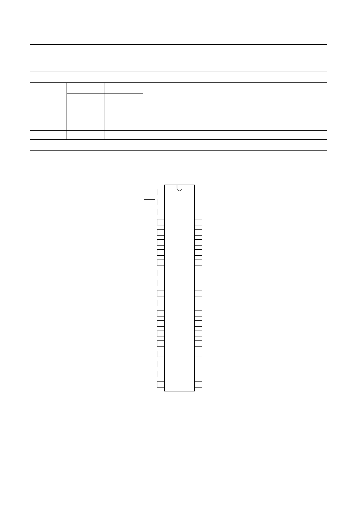
Fig.2 Pin configuration.
2001 Aug 24 6
Page 7

Philips Semiconductors Product specification
Speech and handsfree IC TEA1098
FUNCTIONAL DESCRIPTION
All data values given in this chapter are typical, except
when otherwise specified.
Supplies
LINE INTERFACE AND INTERNAL SUPPLY (PINS LN, SLPE,
REG AND VBB)
Thesupply for theTEA1098 and itsperipheralsis obtained
from the line. The IC generates a stabilized reference
voltage (V
) between pins SLPE and GND. This
ref
reference voltage is equal to 3.7 V for line currents below
18 mA. When the line current rises above 45 mA, the
reference voltage rises linearly to 6.1 V. For line currents
below9 mA,V
isautomaticallyadjusted to alowervalue.
ref
The performance of the TEA1098 in this so-called low
voltage area is limited (see Section “Low voltage
behaviour”). The reference voltage is temperature
compensated.
The voltage between pins SLPE and REG is used by the
internal regulator to generate the stabilized reference
voltage and is decoupled by a capacitor connected
between pins LN and REG. This capacitor, converted into
an equivalent inductance realizes the set impedance
conversionfrom its DC value(R
)to its AC value(done
SLPE
by an external impedance).
The IC regulates the line voltage at pin LN which can be
calculated as follows:
V
V
LN
I
SLPEIlineILN
refRSLPEISLPE
×+=
–=
where:
I
= line current
line
ILN= current consumed on pin LN (approximately a
few µA)
I
= current flowing through the R
SLPE
The preferred value for R
is 20 Ω. Changing this value
SLPE
SLPE
resistor.
not only affects the DC characteristics, it also influences
the transmit gains to the line, the gain control
characteristic,the sidetonelevel, and themaximum output
swing on the line.
Figure 3 shows that the internal circuit is supplied by
pin V
, whichcombined with the line interface is a strong
BB
supply point.
The line current through resistor R
is sunk by the
SLPE
VBBvoltage stabilizer, and is suitable for supplying a
loudspeaker amplifieror any peripheral IC. VBBis 3.0 Vat
line currents below 18 mA and rises linearly to 5.3 V when
the line current rises above 45 mA. It is temperature
compensated.
The current switch (TR1 and TR2) is intended to reduce
distortionof large AC linesignals. Current I
SLPE
issupplied
to VBB via TR1 when the voltage on pin SLPE is above
VBB+ 0.25 V. Whenthe voltage on pin SLPE is below this
value, I
Voltage V
is shunted to GND via TR2.
SLPE
can be increased by connecting an external
ref
resistor between pins REG and SLPE. For large line
currents, this increase can slightly affect some dynamic
performances such as maximumsignal level on the line at
THD = 2%. The external resistor does not affect the
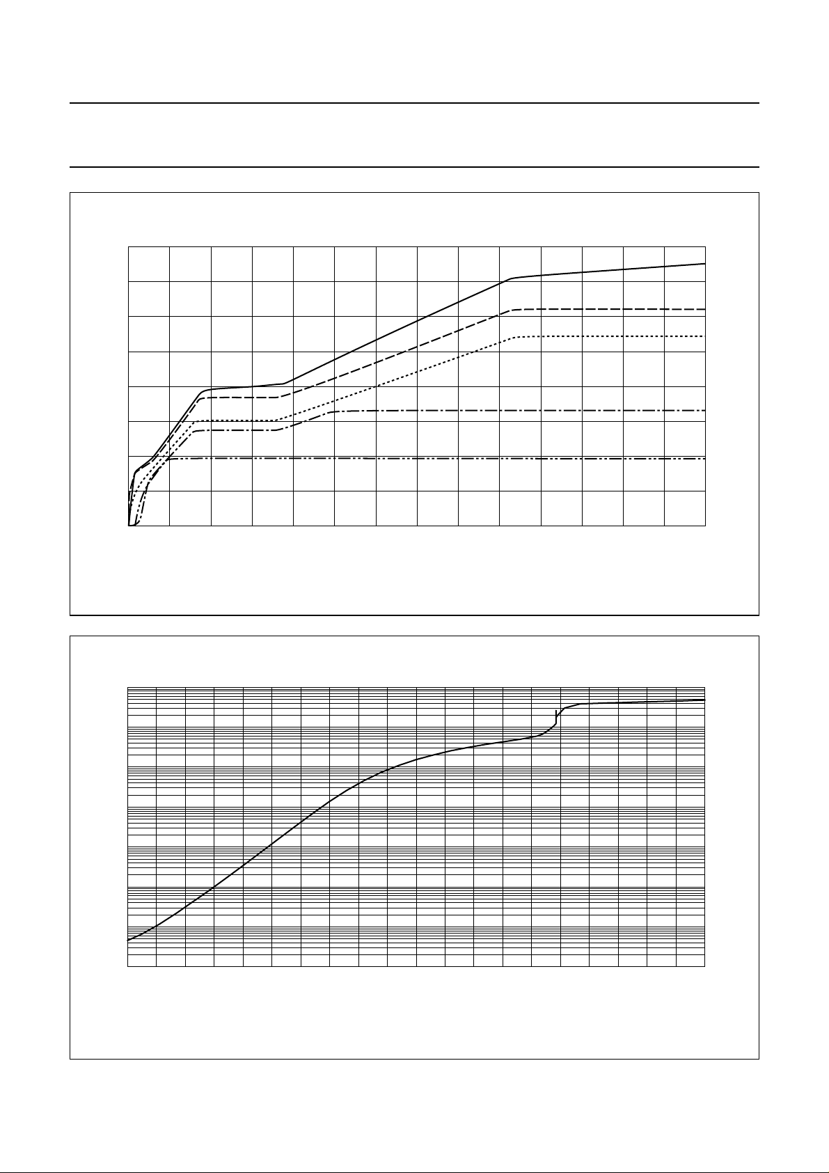
voltage on pin VBB; see Fig.4 for the main DC voltages.
V
SUPPLY FOR MICROCONTROLLERS (PIN V
DD
The voltage on the V
supply point follows the voltage on
DD
DD
)
VBBwith a difference typically of 250 mV, internallylimited
to 3.35 V. This voltage is temperature compensated. This
supply point can provide a current of up to typically 3 mA.
Itsinternal consumption stayslow (a few 10 nA)as long as
VDD does not exceed 1.5 V (see Fig.5).
An external voltage can be connected to VDD with limited
extra consumptionon VDD(typically 100 µA).This voltage
source should not be below 3.5 V or above 6 V.
VBBand VDDcan supply current to external circuits within
the line limits, taking into account the internal current
consumption.
2001 Aug 24 7
Page 8

Philips Semiconductors Product specification
Speech and handsfree IC TEA1098
handbook, full pagewidth
LN
REG
GND
C
REG
4.7 µF
SLPE
TP1
R3
R2
TN1
R1
from
preamp
R
SLPE
20 Ω
J1
Fig.3 Line interface principle.
SUPPLY FOR MICROPHONE (PINS MICS AND GNDTX)
The MICS output can be used as a supply for an electret
microphone. Its voltage is equal to 2.0 V; it can source a
current of up to 1 mA and has an output impedance equal
to 200 Ω.
LOW VOLTAGE BEHAVIOUR
For line currents below 9 mA, the reference voltage is
automatically adjusted to a lower value; the VBB voltage
follows the SLPE voltagewith adifference of250 mV. Any
excess current available, other than for the purposes of
DC biasing the IC, will be small. At low reference voltage,
the IC has limited performance.
When voltage VBB falls below 2.7 V, it is detected by the
receive dynamic limiter circuit connected to pin LSAOand
is continuously activated, discharging the capacitor
connected to pin DLC. In the DC condition, the
loudspeaker is then automatically disabled below this
voltage.
TR2
GND
D1
TR1
E1
TN2
J2
GND
E2
MGM298
D1
V
BB
When VBBfalls below 2.5 V, the TEA1098 is forced into a
lowvoltage mode irrespectiveof the logicinput levels. This
is a speech mode with reduced performance which only
enables the microphone channel (between the MICinputs
and pin LN) and the earpiece amplifier. These two
channels are able to deliver signals for line currents as
small as 3 mA. The HFC input is tied to GND sinking a
current of typically 300 µA.
POWER-DOWN MODE (PIN PD)
To reduce consumption during dialling or register recall
(flash), the TEA1098 is provided with a power-down input
(pin PD). Whenthe voltage on pin PD is LOW, the current
consumption from VBB and VDD is reduced to typically
460 µA. Therefore a capacitor of 470 µF on VBB is
sufficient to power the TEA1098 during pulse dialling or
flash. The PD input has a pull-up structure. In this mode,
the capacitor C
is internally disconnected.
REG
2001 Aug 24 8
Page 9
Philips Semiconductors Product specification
Speech and handsfree IC TEA1098
handbook, full pagewidth
8
voltages
(V)
6
4
2
0
0 0.01
0.02 0.05
0.040.03
Fig.4 Main DC voltages.
I
line
FCA049
SLPE
V
V
MICS
(A)
LN
BB
DD
0.070.06
8
10
handbook, full pagewidth
I
DD
(pA)
7
10
6
10
5
10
4
10
3
10
2
10
10
1.0
FCA050
1.5 2.5 3.0
2.0
VDD (V)
Fig.5 Current consumption on VDD.
2001 Aug 24 9
Page 10

Philips Semiconductors Product specification
Speech and handsfree IC TEA1098
Transmit channels (pins MIC+, MIC−, DTMF, HFTX
and LN)
HANDSET MICROPHONE AMPLIFIER (PINS MIC+, MIC−
AND LN)
The TEA1098 has symmetrical microphone inputs. The
input impedance between pins MIC+ and MIC−is typically
70 kΩ. The voltage gainbetween pins MIC+/MIC−and LN
isset to44.3 dB. Without outputlimitation, themicrophone
input stage can accept signals of up to 18 mV (RMS) at
THD = 2% (room temperature). The microphone inputs
are biased at a voltage of one diode.
Automatic gain control is provided for line loss
compensation.
DTMF AMPLIFIER (PINS DTMF, LN AND RECO)
TheTEA1098 hasan asymmetrical DTMFinput. Theinput
impedance between DTMF and GND is typically 20 kΩ.
The voltage gain between pins DTMF and LN is set to
25.35 dB. Without output limitation, the input stage can
accept signals of up to180 mV (RMS) atTHD = 2% (room
temperature).
When the DTMF amplifier is enabled, dialling tones may
be sent on the line. These tones can be heard in the
earpiece or in the loudspeaker ata lowlevel. This is called
the confidence tone. The voltage attenuation between
pins DTMF and RECO is typically −16.5 dB. This input is
DC biased at 0 V.
The automatic gain control has no effect on these
channels.
HANDSFREE TRANSMIT AMPLIFIER (PINS HFTX AND LN)
The TEA1098 has an asymmetrical HFTX input, which is
mainly intended for use in combination with the TXOUT
output. The input impedance between HFTX and GND is
typically 20 kΩ. The voltage gain between pins HFTX
and LN is set to 34.7 dB. Without output limitation, the
input stage can accept signals of up to 95 mV (RMS) at
THD = 2% (room temperature).
Receive channels (pins IR, RECO, GARX and QR)
RX AMPLIFIER (PINS IR AND RECO)
The receive amplifier has one input (IR) which is
referenced to the line. The input impedance between pins
IR and LN is typically 20 kΩ and the DC bias between
these pins is equal to the voltage of one diode. The gain
between pins IR(referenced to LN) and RECO is typically
29.7 dB. Without output limitation, the input stage can
accept signals of up to 50 mV (RMS) at THD = 2% (room
temperature).
The receive amplifier has a rail-to-rail output (RECO),
which is designed for use with high ohmic (real) loads of
more than 5 kΩ. This output is biased at a voltage of two
diodes.
Automatic gain control is provided for line loss
compensation.
EARPIECE AMPLIFIER (PINS GARX AND QR)
The earpiece amplifier is an operational amplifier which
hasan output (QR)andaninverting input (GARX).Itsinput
signal is fed by a decoupling capacitor from the receive
amplifier output (RECO) to two resistors which set the
required gain or attenuation from −3 to +15 dB compared
to the receive gain.
Two external capacitors C
and QR) and C
ensure stability. The C
(connected between GAR and GND)
GARS
GAR
(connected between GAR
GAR
capacitor provides a first-order
low-pass filter. The cut-off frequency corresponds to the
time constant C
C
≥ 10 × C
GARS
× Re2. The relationship
GAR
must be satisfied.
GAR
The earpiece amplifierhas arail-to-rail output(QR) biased
at a voltage of two diodes. It is designed for use with low
ohmic (real) loads of 150 Ω, or capacitive loads of 100 nF
in series with 100 Ω.
The HFTX input is biased at a voltage of two diodes.
Automatic gain control is provided for line loss
compensation.
2001 Aug 24 10
Page 11
Philips Semiconductors Product specification
Speech and handsfree IC TEA1098
AGC (pin AGC)
The TEA1098 performsautomatic lineloss compensation,
which fits well with the true line attenuation. The automatic
gain control varies the gain of some transmit and receive
amplifiers in accordance with the DC line current. The
control range is6.45 dB forG
6.8 dB for G
v(HFTX-LN)
, which corresponds approximately
v(MIC-LN)
and G
v(IR-RECO)
, and
to a line length of 5.5 km for a 0.5 mm twisted-pair copper
cable.
To enable this gain control, pin AGC must be shorted to
pin LN. The start currentfor compensationcorresponds to
a line current of typically 23 mA and a stop current of
57 mA. The start current can be increased by connecting
an external resistor between pins AGC and LN. It can be
increased by up to 40 mA (using a resistor of typically
80 kΩ). The start and stop current will be maintained at a
ratio of 2.5. By leaving pin AGC open, the gain control is
disabled and no line loss compensation occurs.
Handsfree application
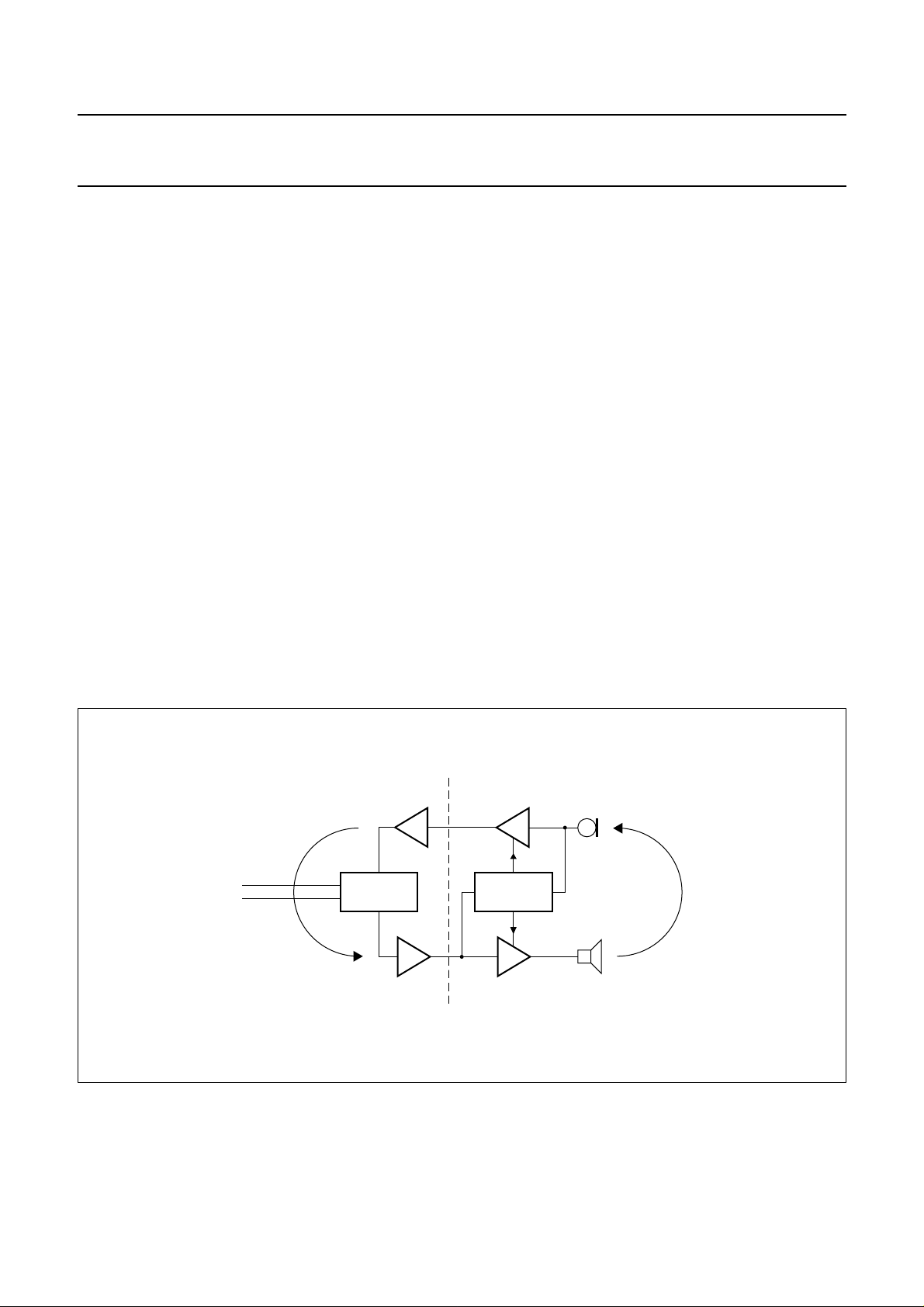
Figure 6 shows a loop is formed by the sidetone network
in the line interface section, and by the acoustic coupling
between loudspeaker and microphone in the handsfree
section. A loop-gain of greater than 1 causes howl.
To prevent howl in full duplex applications, the loop-gain
must be set much lower than 1. This is achieved by the
duplex controller which detects the channel with the
‘largest’ signal and controls the gains of the microphone
and the loudspeaker amplifiers so that the sum of their
gains remains constant.
Thereforein the handsfreeapplication,thecircuit can have
three stable modes:
1. Transmit mode (Tx mode):
The microphone amplifieris atmaximum gain, andthe
loudspeaker amplifier is at minimum gain.
2. Receive mode (Rx mode):
The microphoneamplifier is at minimum gain, and the
loudspeaker amplifier is at maximum gain.
3. Idle mode:
The microphone amplifier and the loudspeaker
amplifier are both midway between maximum and
minimum gain.
The difference between the maximum and minimum gain
is called the switching range.
handbook, full pagewidth
telephone
line
sidetone
HYBRID
Fig.6 Handsfree telephone set principles.
2001 Aug 24 11
acoustic
coupling
DUPLEX
CONTROL
MGM299
Page 12
Philips Semiconductors Product specification
Speech and handsfree IC TEA1098
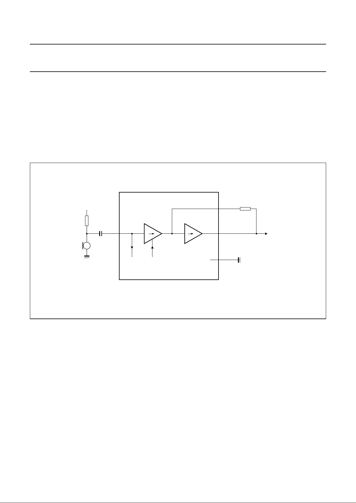
HANDSFREE MICROPHONE CHANNEL (PINS TXIN, GATX,
TXOUT AND GNDTX; See Fig.7)
TheTEA1098 has an asymmetricalhandsfreemicrophone
input (TXIN) with an input resistance of 20 kΩ.
The input DCbias is 0 V.Thegain oftheinput stage varies
according to the TEA1098 mode. In Tx mode, it has
maximum gain; in Rx mode, it has minimum gain, and in
Idle mode, it is midway between maximum and minimum
gain.
handbook, full pagewidth
V
BB
R
MIC
C
MIC
TXIN
31
envelope
detector
V I I V
to
from
voice
switch
Switch-over from one mode to the other is smooth and
click-free. The output (TXOUT) is biased at a voltage of
two diodes and has a current capability of 20 µA (RMS).
In Tx mode, the overall gain of the microphone amplifier
(from pins TXIN to TXOUT) can be adjusted from
0 up to 31 dB to suit specific application requirements.
The gain is proportional to the value of R
15.2 dB when R
is 30.1 kΩ. Without output limitation,
GATX
GATX
and equals
the microphone input stage can accept signals of up to
18 mV (RMS) at THD = 2% (room temperature).
R
30
29
32
GATX
TXOUT
GNDTX
GATX
Fig.7 Handsfree microphone channel.
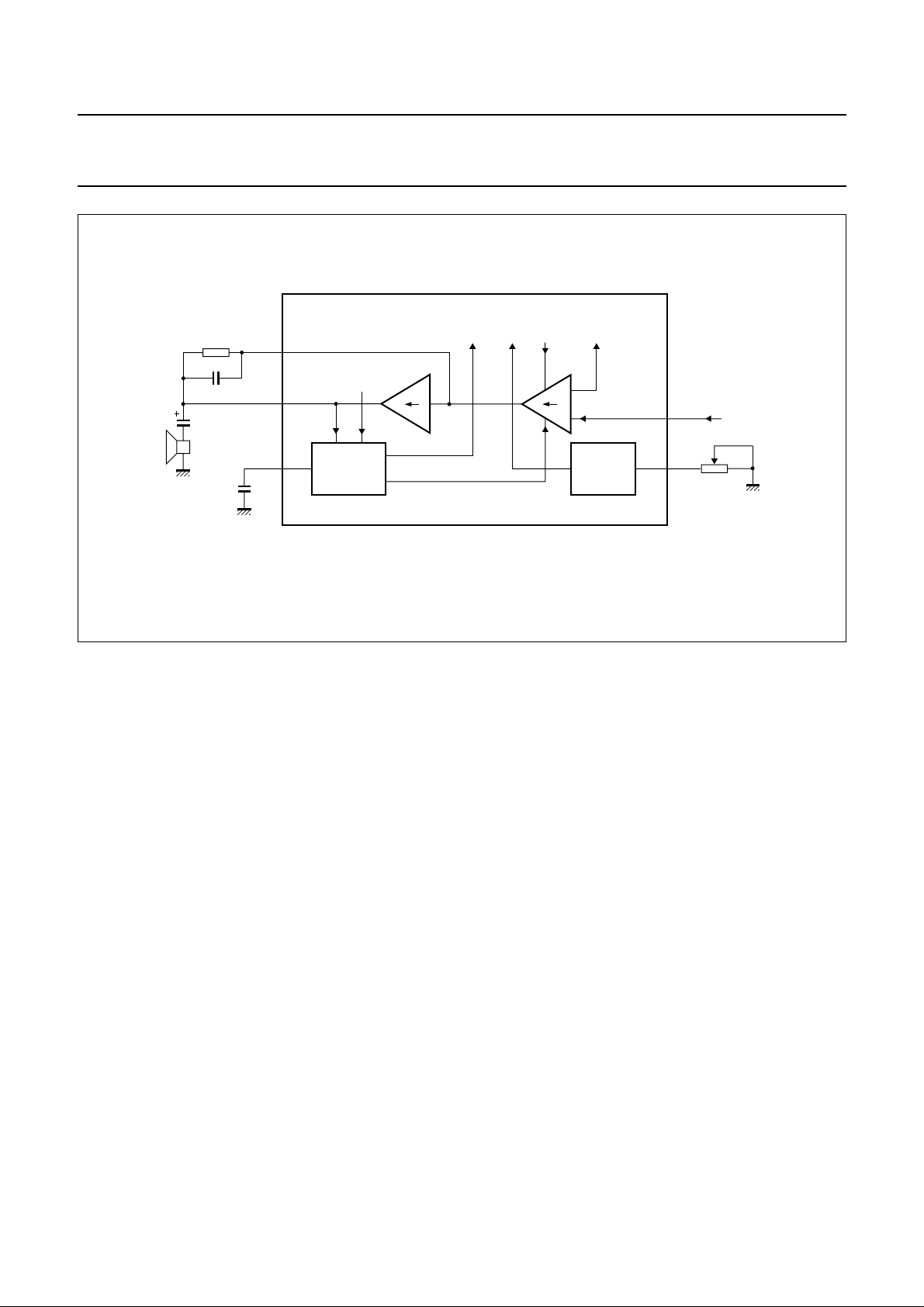
LOUDSPEAKER CHANNEL
Loudspeaker amplifier (pins HFRX, GALS and LSAO)
The TEA1098 loudspeaker amplifier has an asymmetrical
input with an input resistance of 20 kΩ between
pins HFRX and GND. It is biased at a voltage of two
diodes. Without output limitation, the input stage can
accept signals of up to580 mV (RMS) atTHD = 2% (room
temperature).
The gain of the input stage varies according to the
TEA1098 mode. In Rx mode, it has maximum gain; in
Tx mode, it has minimum gain and in Idle mode, it is
halfway between maximum and minimum gain.
Switch-over from one mode to the other is smooth and
click-free.The rail-to-rail outputstageis designedtopower
aloudspeaker connected asasingle-ended load (between
pins LSAO and GND).
MGL342
In Rx mode, the overall gain of the loudspeaker amplifier
can be adjusted from 0 up to 35 dB to suit specific
application requirements. The gain from pin HFRX to
pin LSAO is proportional to the value of R
28 dB when R
is 255 kΩ. It is recommended that a
GALS
capacitor is connected in parallel with R
GALS
to provide a
GALS
and is
first-order low-pass filter.
Volume control (pin VOL)
The loudspeaker amplifier gain can be adjusted by the
potentiometer R
potentiometer canbe used. Each 1.9 kΩ increase of R
. For logarithmic gain control, a linear
VOL
VOL
resultsin again loss of 3 dB. Themaximum gainreduction
using the volume control is internally limited to the
switching range (see Fig.8).
2001 Aug 24 12
Page 13
Philips Semiconductors Product specification
Speech and handsfree IC TEA1098
handbook, full pagewidth
R
GALS
GALS
14
V
C
C
LSAO
GALS
C
DLC
LSAO
DLC
15
12
BB
V I
DYNAMIC
LIMITER
Fig.8 Loudspeaker channel.
Dynamic limiter (pin DLC)
The TEA1098 dynamic limiter prevents clipping of the
loudspeakeroutput stageandprotects theoperationof the
circuit when the supply voltage at VBB falls below 2.7 V.
Hardclipping ofthe loudspeaker outputstage isprevented
by rapidly reducing the gain when the output stage starts
to saturate. The time taken to effect gain reduction
(clipping attack time) is approximately a few milliseconds.
The circuit stays in the reduced gain mode until the peaks
ofthe loudspeaker signalsnolonger causesaturation.The
gain of the loudspeaker amplifier then returns to its normal
value within the clipping release time (typically 250 ms).
Bothattack andrelease times areproportional tothe value
of the capacitor C
DLC
.
The total harmonic distortion of the loudspeaker output
stage, in reduced gain mode, stays below 2% up to 10 dB
(minimum) of input voltage overdrive providing V
HFRX
is
below 580 mV (RMS).
When the supply voltage falls below an internal threshold
voltage of 2.7 V, the gain of the loudspeaker amplifier is
reduced rapidly (approximately 1 ms). When the supply
voltage rises above 2.7 V, the gain of the loudspeaker
amplifier is increased. By forcing a level lower than 0.2 V
on pin DLC, the loudspeaker amplifier is muted and the
TEA1098 is automatically forced into the Tx mode.
to
logic
to/from
voice switch
I V
to
envelope
detector
VOLUME
CONTROL
26
MGL343
5
HFRX
VOL
R
VOL
DUPLEX CONTROLLER
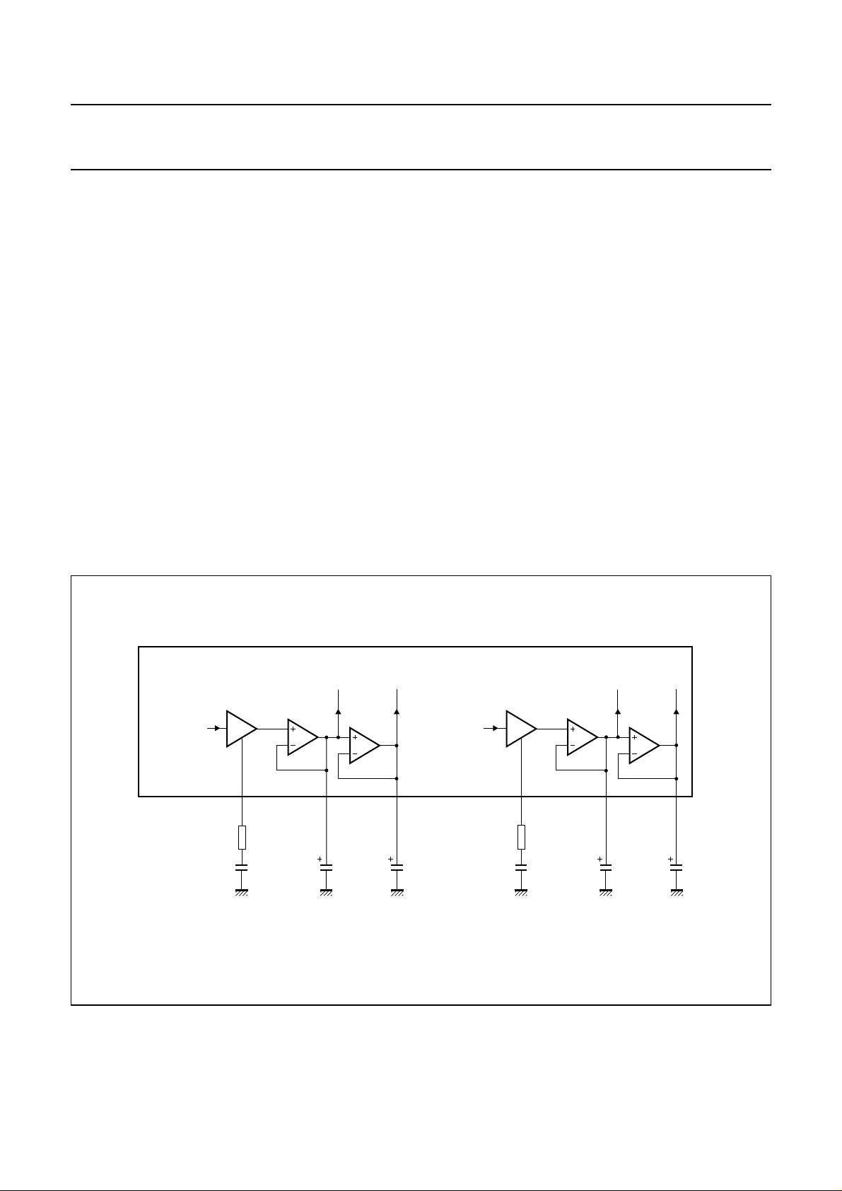
Signal and noise envelope detectors (pins TSEN, TENV,
TNOI, RSEN, RENV and RNOI)
The strength of signal level and background noise in both
channels is monitored by signal envelope detectors and
noise envelope detectors respectively. The outputs of the
envelope detectors provide inputs to the decision logic.
The signal and noise envelope detectors are shown in
Fig.9.
For the transmitchannel, thesignal betweenpin TXIN and
pin TSEN is amplified by 40 dB. For the receive channel,
the signal between pin HFRX and pin RSEN is amplified
by 0 dB.
The signals between pin TSEN and pin TENV, and
between pin RSEN and pin RENV are logarithmically
compressed and buffered.
The sensitivity of the envelope detectors is set by
resistors R
TSEN
and R
. The capacitors connected in
RSEN
series with these two resistors block any DC component
and form a first-order high-pass filter.
In the basic application (see Fig.17) it is assumed that
V
= 1 mV (RMS) and V
TXIN
and R
capacitors C
TSEN
and R
TSEN
both have a value of 10 kΩ. When
RSEN
and C
RSEN
= 100 mV (RMS) nominal
HFRX
both have a value of 100 nF,
the cut-off frequency is at 160 Hz.
2001 Aug 24 13
Page 14
Philips Semiconductors Product specification
Speech and handsfree IC TEA1098
The buffer amplifiers feeding the compressed signals to
pins TENV and RENV have a maximum source current of
120 µA and a maximum sink current of 1 µA. Capacitors
C
TENV
and C
set the timing of both signal envelope
RENV
detectors. In the basic application, the value of both
capacitors is 470 nF. Because of the logarithmic
compression, each6 dB signal increase means an 18 mV
increase on the signal envelopes at pins TENV or RENV
(room temperature). Thus, timings can be expressed
in dB/ms. At room temperature, the 120 µA sourced
current corresponds to a maximum signal envelope
rise-slope of 85 dB/ms, which is sufficient to track normal
speech signals. The 1 µA current sunk by pin TENV or
pin RENV corresponds to a maximum fall-slope of
0.7 dB/ms. This is sufficient for a smooth envelope and
also eliminates the effect of echoes on switching
behaviour.
To determine the noise level, the signals between pin
TENV and pin TNOI, and between pin RENV and pin
RNOI are buffered. The buffers have a maximum source
current of 1 µA and a maximum sink current of 120 µA.
Capacitors C
TNOI
and C
set the timing of both noise
RNOI
envelope detectors. In the basic application (see Fig.17)
the value of both capacitors is 4.7 µF.
At room temperature, the 1 µA sourced current
corresponds to a maximum noise envelope rise-slope of
approximately 0.07 dB/ms which is small enough to track
background noise without being affected by speech
bursts.
The 120 µA sink current corresponds to a maximum
fall-slope of approximately 8.5 dB/ms. However, because
the noiseenvelope tracks thefall of the signal envelope, it
will never fall faster than approximately 0.7 dB/ms. The
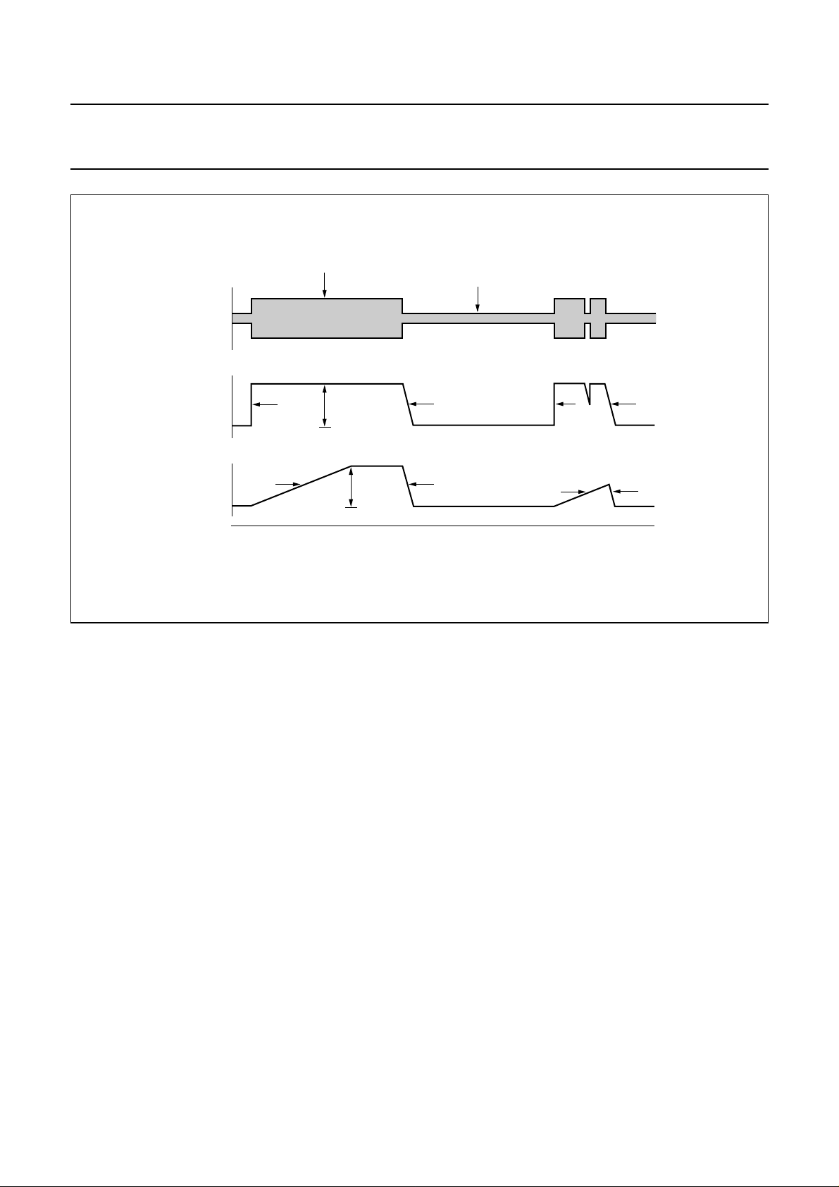
behaviour of the signal envelope and noise envelope
detectors is illustrated in Fig.10.
handbook, full pagewidth
DUPLEX CONTROLLER
from
microphone
amplifier
to logicto logic
LOG
from
loudspeaker
amplifier
876 10119
TSEN
R
C
TENV TNOI RSEN RENV RNOI
TSEN
TSEN
C
TENV
C
TNOI
LOG
R
RSEN
C
RSEN
C
RENV
C
RNOI
MGL344
Fig.9 Signal and noise envelope detectors.
2001 Aug 24 14
Page 15
Philips Semiconductors Product specification
Speech and handsfree IC TEA1098
C
4 mV (RMS)
A
36 mV
36 mV
handbook, full pagewidth
INPUT SIGNAL
SIGNAL ENVELOPE
A: 85 dB/ms
B: 0.7 dB/ms
NOISE ENVELOPE
B: 0.7 dB/ms
C: 0.07 dB/ms
Fig.10 Signal and noise envelope waveforms.
Decision logic (pins IDT and SWT)
The TEA1098 selects its mode of operation
(Tx, Rx or Idle) by comparing the signal and noise
envelopes of both channels. This is executed by the
decision logic. The resulting voltage on pin SWT is the
input to the voice switch.
To facilitate the distinction between signal and noise, the
signal is considered as speech when its envelope is more
than 4.3 dB above the noise envelope. At room
temperature, this is equal to a voltage difference of
V
− V
ENV
= 13 mV. This so called speech/noise
NOI
threshold is implemented in both channels.
The signal on pin TXIN contains both speech and the
acoustically coupled signal from the loudspeaker. In
Rx mode, the loudspeaker signal overrides the speech.
Therefore, the signal envelope on pin TENV consists
mainly of the loudspeaker signal. To correct this, an
attenuator is connected between pin TENV and the
TENV/RENV comparator. Its attenuation is equal to that
applied to the microphone amplifier.
MBG354
1 mV (RMS)
B
B
A
C
B
B
time
To prevent this, a dial tone detector monitorsinput signals
between pins HFRX and GND. In standard applications,
the detector does not consider a signal level above
25 mV (RMS) to be noise. This level is proportional to the
value of R
. Similarly, a transmit detector monitors
RSEN
input signals between pins TXINand GNDTX. In standard
applications the detector does not consider a signal level
above 0.75 mV (RMS) to be noise. This level is
proportional to the value of R
TSEN
.
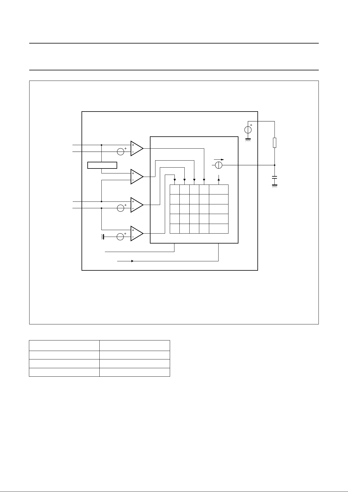
Figure 11 shows that the output of the decision logic is a
current source. The logic table shows the relationship
between the input levels and the value of the current
source. The current source can charge or discharge the
capacitor C
at a switch-over current of 10 µA. If the
SWT
current is zero, the voltage on pin SWT becomes equal to
the voltage on pin IDT via the high-ohmic resistor R
IDT
(idling). The resulting voltage difference between
pins SWT and IDT can vary between −400 and +400 mV
and determines the TEA1098 mode (see Table 1).
Whena dialtone is present on theline, withoutmonitoring,
it would be recognized as noise because it has a constant
amplitude. This would cause the TEA1098 to go into Idle
mode, and the user would hear the dial tone fade away.
2001 Aug 24 15
Page 16
Philips Semiconductors Product specification
Speech and handsfree IC TEA1098
handbook, full pagewidth
TENV
TNOI
RENV
RNOI
7
6
ATTENUATOR
11
9
from logic
from dynamic
limiter
13 mV
13 mV
V
dt
DUPLEX CONTROLLER
LOGIC
XX11−10 µA
X10X
1X0X
XX10 0
000X 0
IDT
28
V
ref
(1)
27
SWT
+10 µA
+10 µA
MGL345
R
C
IDT
SWT
(1) When DLC < 0.2 V thecurrent of −10 µA is forced.
Fig.11 Decision logic.
Table 1 TEA1098 modes
V
− V
SWT
(mV) MODE
IDT
<−180 Tx mode
0 Idle mode
>180 Rx mode
SWT
SWT
and
and
The switch-over timing can be set by capacitor C
the Idle mode timing can be set by capacitor C
resistor R
C
SWT
. In the basic application given in Fig.17,
IDT
is 220 nF and R
is 2.2 MΩ. This enables a
IDT
switch-over time from Tx to Rx mode or vice-versa of
approximately 13 ms (580 mV swing on pin SWT). The
switch-over time from Idle mode to Tx or Rx mode is
approximately 4 ms (180 mV swing on pin SWT).
2001 Aug 24 16
The switch-over time, from Rx or Tx mode to Idle mode is
equal to 4 × R
IDT
× C
and is approximately 2 s (Idle
SWT
mode time).
The DLC input overrides the decision logic. When the
voltage on pin DLC falls below 0.2 V, the capacitor C
SWT
is discharged by 10 µA which selects Tx mode.
Page 17
Philips Semiconductors Product specification
Speech and handsfree IC TEA1098
Voice switch (pins STAB and SWR)
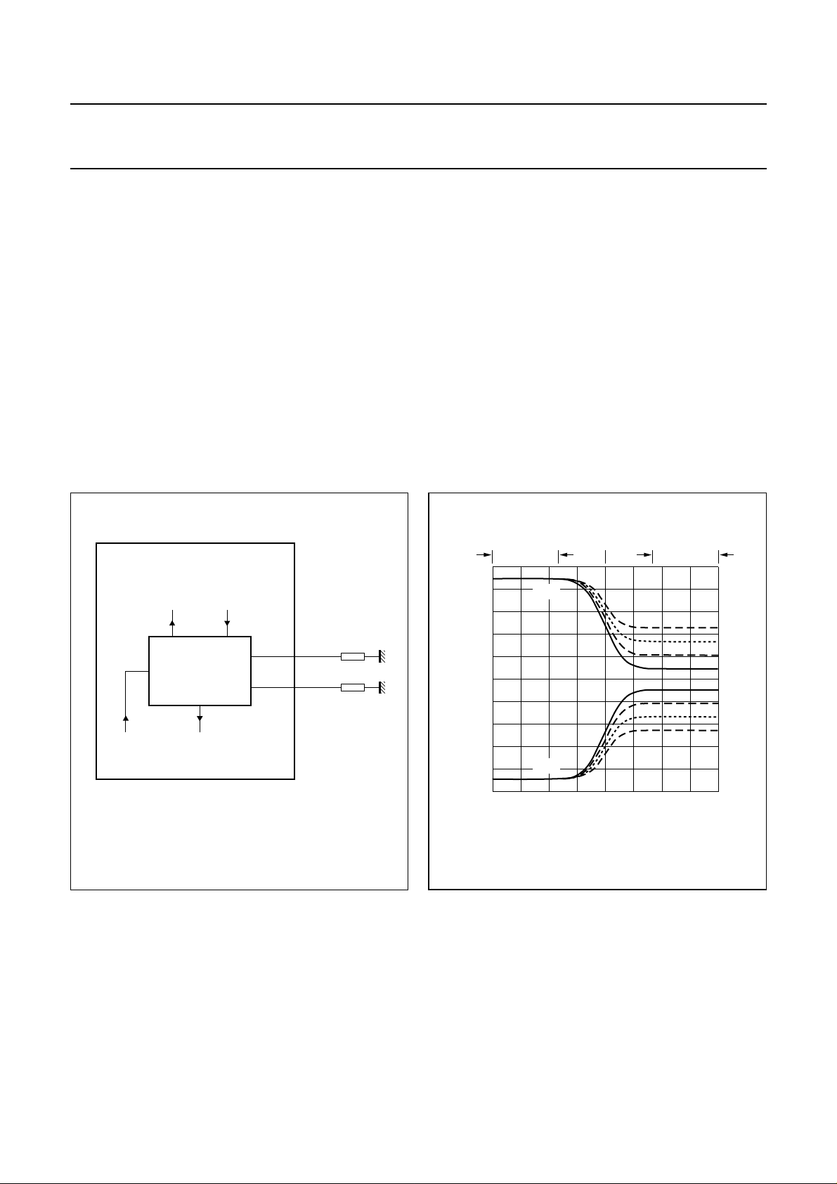
Figure 12 is a diagram of the voice switch. With a voltage
onpin SWT, the TEA1098voiceswitchregulates the gains
of the transmitand thereceive channelsso thatthe sum of
both is held constant.
In Tx mode, the microphone amplifier is at maximum gain
and the loudspeaker amplifier is at minimum gain.
In Rx mode, their gains are the opposite. In Idle mode,
both microphone and loudspeaker amplifiers are midway
between maximum and minimum gain.
The difference between the maximum and minimum gain
is called the switching range. This range is determined by
the ratio of resistors R
between 0 and 52 dB. Resistor R
SWR
to R
and is adjustable
STAB
should be 3.65 kΩ
STAB
which sets an internally used reference current.
alfpage
DUPLEX CONTROLLER
to
microphone
amplifier
from
SWT
Inthebasic application diagram (seeFig.17)resistor R
SWR
is 365 kΩwhich results in a switching range of 40 dB. The
switch-over behaviour is illustrated in Fig.13.
In Rx mode, the gain of the loudspeaker amplifier can be
reduced using the volume control. At the same time, the
gainof the microphoneamplifierincreases, sincethevoice
switch keeps the sum of the gains constant (see dashed
curves in Fig.13). However, in Tx mode, the volume
control has no effect on the gains of the microphone or
loudspeakeramplifiers.Consequently,theswitchingrange
is reduced when the volume is reduced. At maximum
reduction of volume, the switching range is 0 dB.
handbook, halfpage
G
G
vrx
vtx,
(10 dB/div)
Idle
Tx mode Rx mode
G
vtx
mode
MGM305
R
VOL
(Ω)
from
volume
control
(1) C = constant.
vrx =
to
(1)
C
G
+ G
vtx
VOICE SWITCH
loudspeaker
amplifier
Fig.12 Voice switch.
24
25
MGL346
STAB
SWR
R
STAB
R
SWR
G
vrx
−400 −200 0 +400+200
V
SWT
Fig.13 Switch-over behaviour.
− V
IDT
(mV)
11400
7600
3800
0
0
3800
7600
11400
2001 Aug 24 17
Page 18
Philips Semiconductors Product specification
Speech and handsfree IC TEA1098
Logic inputs
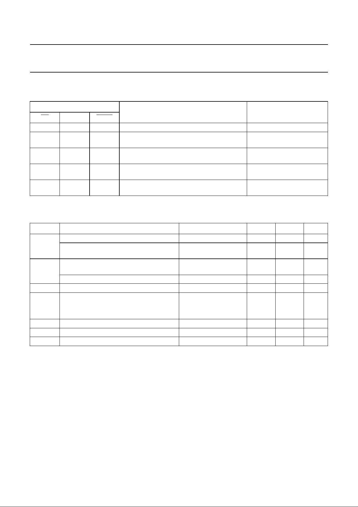
Table 2 Selection of transmit and receive channels for 5 different application modes
LOGIC INPUTS
FEATURES APPLICATION EXAMPLES
PD HFC MUTE
0 X X flash; DC dialling
1 0 0 DTMF to LN; DTMF to RECO; QR and MICS are
active
1 0 1 MICS to LN; IR to RECO; QR and MICS are
DTMF dialling in handset
mode
handset conversation mode
active
1 1 0 DTMF to LN; DTMF to RECO; HFRX to LSAO;
QR and MICS are active
1 1 1 TXIN to TXOUT; HFTX to LN; IR to RECO;
DTMF dialling in handsfree
mode
handsfree conversation mode
HFRX to LSAO; MICS is active
LIMITING VALUES
In accordance with the Absolute Maximum Rating System (IEC 60134); all DC levels are referenced to GND.
SYMBOL PARAMETER CONDITIONS MIN. MAX. UNIT
V
LN
positive continuous line voltage −0.4 +12 V
repetitive line voltage during switch-on or line
−0.4 +13.2 V
interruption
V
n(max)
maximum voltage on pins REG, SLPE, IR
−0.4 VLN+ 0.4 V
and AGC
−0.4 VBB+ 0.4 V
I
P
T
T
T
line
tot
stg
amb
j
maximum voltage on all other pins except V
DD
maximum line current − 130 mA
total power dissipation
TEA1098TV T
TEA1098UH T
=75°C; see Fig.14 − 400 mW
amb
=75°C; note 1 −−mW
amb
storage temperature −40 +125 °C
ambient temperature −25 +75 °C
junction temperature − 125 °C
Note
1. Mostly dependent on the maximum required ambienttemperature, on the voltage between LN and SLPEand on the
thermal resistance between dieand ambienttemperature. Thisthermal resistance depends on the application board
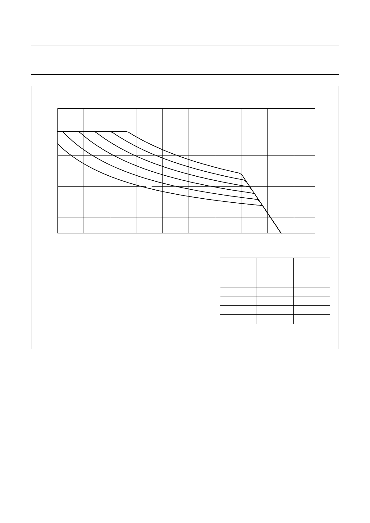
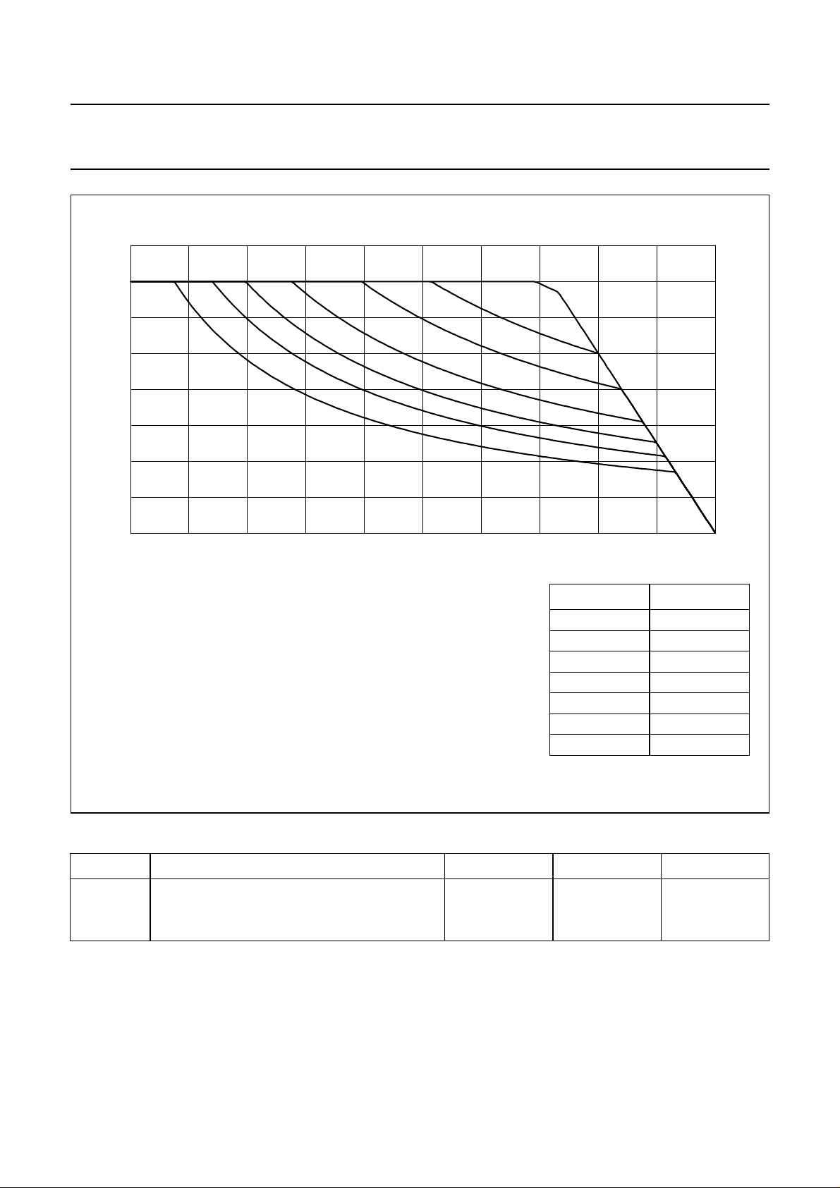
layoutand onthe materials used.Figure 15 showsthe safe operating area versusthis thermal resistance for ambient
temperature T
amb
=75°C.
2001 Aug 24 18
Page 19
Philips Semiconductors Product specification
Speech and handsfree IC TEA1098
160
handbook, full pagewidth
I
line
(mA)
120
80
40
0
3.5 9.5
FCA028
(1)
(2)
(3)
(4)
(5)
(6)
7.55.5
CURVE T
11.5
amb
V
SLPE
(°C) P
(V)
tot
13.5
(mW)
(1) 25 790
(2) 35 710
(3) 45 630
(4) 55 550
(5) 65 470
(6) 75 390
Fig.14 Safe operating area of the TEA1098TV.
2001 Aug 24 19
Page 20
Philips Semiconductors Product specification
Speech and handsfree IC TEA1098
160
handbook, full pagewidth
I
line
(mA)
120
80
40
0
246
FCA079
(1)
(2)
(3)
(4)
(5)
(6)
(7)
810
CURVE R
V
SLPE
(V)
th(j-a)
(1) 40
(2) 50
(3) 60
(4) 75
(5) 90
(6) 105
(7) 130
12
(K/W)
Fig.15 Safe operating area of the TEA1098UH at T
amb
=75°C.
THERMAL CHARACTERISTICS
SYMBOL PARAMETER CONDITIONS VALUE UNIT
R
th(j-a)
thermal resistance from junction to ambient
TEA1098TV in free air 117 K/W
TEA1098UH note 1 − K/W
Note
1. The value is to be determined by the customer in the application.
2001 Aug 24 20
Page 21
Philips Semiconductors Product specification
Speech and handsfree IC TEA1098
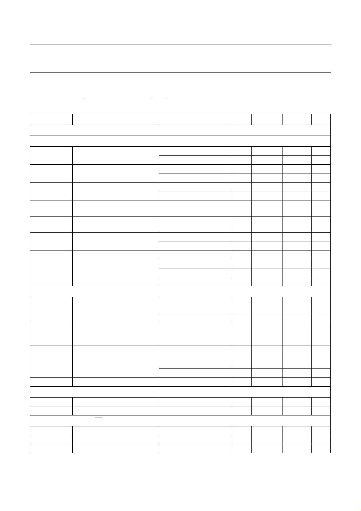
CHARACTERISTICS
I
= 15 mA; R
line
connected to pin LN;
referenced to GND; unless otherwise specified.
SYMBOL PARAMETER CONDITIONS MIN. TYP. MAX. UNIT
Supplies
SLPE
=20Ω;Z
= 600 Ω; f = 1 kHz;T
line
=25°C forTEA1098TV;Tj=25°C forTEA1098UH; pin AGC
amb
PD = HIGH; HFC = LOW; MUTE = HIGH; measured according to test circuit; all DC levels are
INE INTERFACE AND INTERNAL SUPPLY (PINS LN, SLPE, REG AND V
L
V
V
I
line
SLPE
BB
stabilized voltage between
pins SLPE and GND
regulated supply voltage for
internal circuitry
I
= 15 mA 3.4 3.7 4 V
line
I
= 70 mA 5.7 6.1 6.5 V
line
I
= 15 mA 2.75 3.0 3.25 V
line
I
= 70 mA 4.9 5.3 5.7 V
line
line current for voltage increase start current − 18 − mA
stop current − 45 − mA
∆V
SLPE(T)
stabilized voltage variation with
T
= −25 to +75 °C −±60 − mV
amb
temperature referenced to 25 °C
∆V
BB(T)
regulated voltage variation with
T
= −25 to +75 °C −±30 − mV
amb
temperature referenced to 25 °C
I
BB
current available on pin V
BB
in speech mode − 11 − mA
in handsfree mode − 9 − mA
V
LN
line voltage I
=1mA − 1.55 − V
line
I
=4mA − 2.35 − V
line
I
= 15 mA 3.7 4.0 4.3 V
line
I
= 130 mA − 8.7 9.5 V
line
SUPPLY FOR PERIPHERALS (PIN VDD)
V
DD
regulated supply voltage on VDDVBB> 3.35 V + 0.25 V
(typ.)
otherwise − V
∆V
DD(T)
regulated voltage variation with
temperature referenced to 25 °C
T
= −25 to +75 °C;
amb
VBB> 3.35 V + 0.25 V
(typ.)
I
DD
current consumption on V
DD
in trickle mode;
I
= 0 mA; VDD= 1.5 V;
line
VBB discharging
V
> 3.35 V 60 100 −µA
DD
I
DD(o)
current available for peripherals VDD= 3.35 V −−3 − mA
SUPPLY FOR MICROPHONE (PIN MICS)
V
MICS
I
MICS
supply voltage for a microphone − 2.0 − V
current available on MICS −− −1mA
POWER-DOWN INPUT (PIN PD)
V
IL
V
IH
I
PD
LOW-level input voltage −0.4 − +0.3 V
HIGH-level input voltage 1.8 − VBB+ 0.4 V
input current −−3 −6 µA
BB
)
3.1 3.35 3.6 V
− 0.25 − V
BB
−±30 − mV
− 15 150 nA
2001 Aug 24 21
Page 22
Philips Semiconductors Product specification
Speech and handsfree IC TEA1098
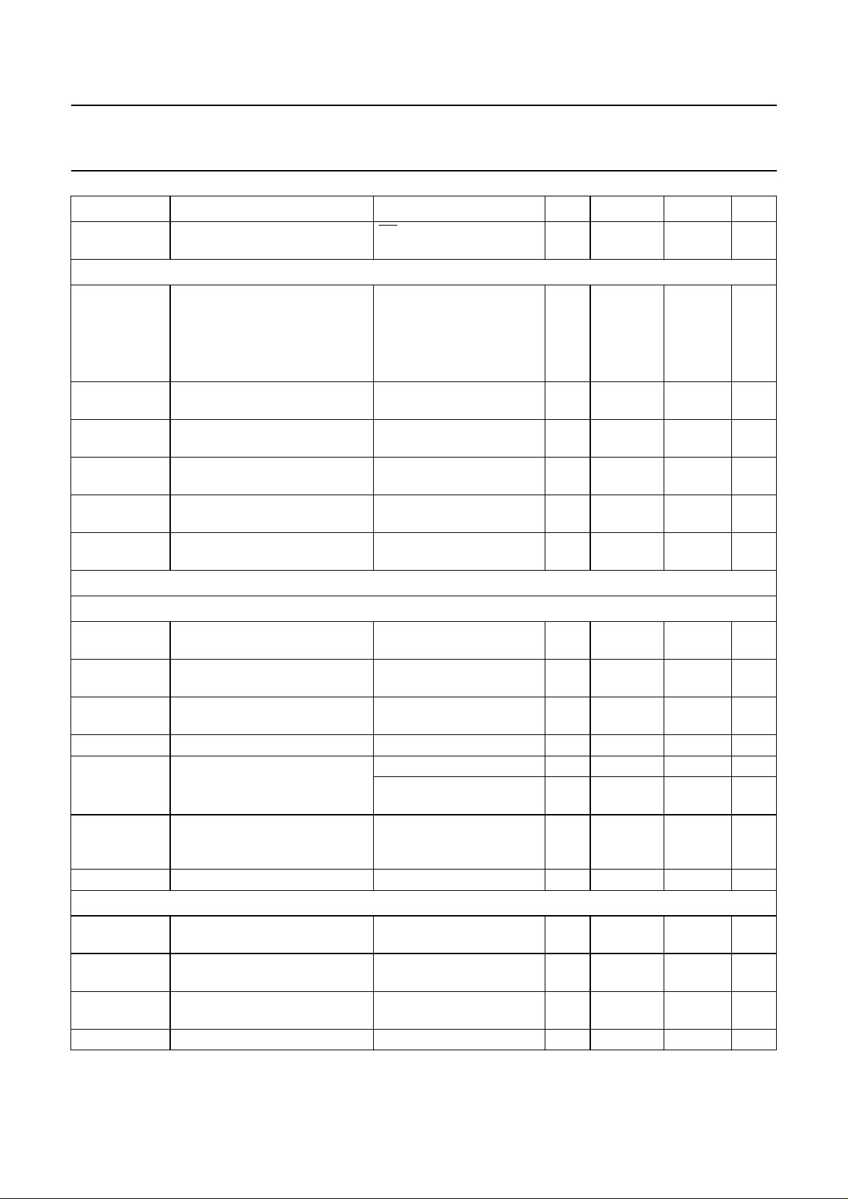
SYMBOL PARAMETER CONDITIONS MIN. TYP. MAX. UNIT
I
BB(PD)
Preamplifier inputs (pins MIC+, MIC−, IR, DTMF, TXIN, HFTX and HFRX)
input impedance
Z
i(MIC)
Z
input impedance between
i(IR)
Z
Z
Z
Z
input impedance between
i(DTMF)
input impedance between
i(TXIN)
input impedance between
i(HFTX)
input impedance between
i(HFRX)
TX amplifiers
current consumption on V
BB
during power-down
differentialbetweenpins MIC+
and MIC−
single-ended between
pins MIC+/MIC− and GNDTX
pins IR and LN
pins DTMF and GND
pins TXIN and GNDTX
pins HFTX and GND
pins HFRX and GND
PD = LOW − 460 −µA
− 70 − kΩ
− 35 − kΩ
− 20 − kΩ
− 20 − kΩ
− 20 − kΩ
− 20 − kΩ
− 20 − kΩ
TX HANDSET MICROPHONE AMPLIFIER (PINS MIC+, MIC− AND LN)
G
v(MIC-LN)
voltage gain from
V
= 5 mV (RMS) 43.3 44.3 45.3 dB
MIC
pins MIC+/MIC− to LN
∆G
v(f)
gain variation with frequency
f = 300 to 3400 Hz −±0.25 − dB
referenced to 1 kHz
∆G
v(T)
gain variation with temperature
T
= −25 to +75 °C −±0.25 − dB
amb
referenced to 25 °C
CMRR common mode rejection ratio − 80 − dB
THD total harmonic distortion at LN VLN= 1.4 V (RMS) −− 2%
I
line
= 4 mA;
−− 10 %
VLN= 0.12 V (RMS)
V
no(LN)
noise output voltage at pin LN;
pins MIC+/MIC− shorted
psophometrically weighted
(p53 curve)
−−77.5 − dBmp
through 200 Ω
∆G
v(mute)
gain reduction if not activated see Table 2 60 80 − dB
DTMF AMPLIFIER (PINS DTMF, LN AND RECO)
G
v(DTMF-LN)
voltage gain from
V
= 50 mV (RMS) 24.35 25.35 26.35 dB
DTMF
pins DTMF to LN
∆G
v(f)
gain variation with frequency
f = 300 to 3400 Hz −±0.25 − dB
referenced to 1 kHz
∆G
v(T)
gain variation with temperature
T
= −25 to +75 °C −±0.25 − dB
amb
referenced to 25 °C
∆G
v(mute)
gain reduction if not activated see Table 2 60 80 − dB
2001 Aug 24 22
Page 23
Philips Semiconductors Product specification
Speech and handsfree IC TEA1098
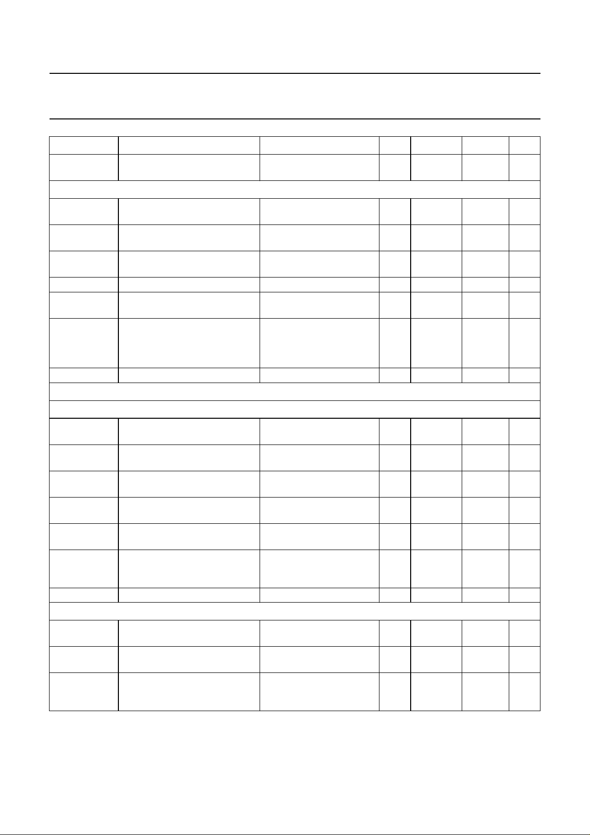
SYMBOL PARAMETER CONDITIONS MIN. TYP. MAX. UNIT
G
v(DTMF-RECO)
TX AMPLIFIER USING HFTX (PINS HFTX AND LN)
G
v(HFTX-LN)
voltage gain from pin DTMF to
RECO
voltage gain from pin HFTX toLNV
V
= 50 mV (RMS) −−16.5 − dB
DTMF
= 15 mV (RMS) 33.5 34.7 35.9 dB
HFTX
∆G
v(f)
gain variation with frequency
referenced to 1 kHz
∆G
v(T)
gain variation with temperature
referenced to 25 °C
THD total harmonic distortion at LN V
V
HFTX(rms)
maximum inputvoltage at HFTX
(RMS value)
V
no(LN)
noise output voltage at pin LN;
pin HFTX shorted to GND
through 200 Ω in series with
10 µF
∆G
v(mute)
gain reduction if not activated see Table 2 60 80 − dB
RX amplifiers
RX AMPLIFIERS USING IR (PINS IR AND RECO)
G
v(IR-RECO)
voltage gain from pin IR
(referenced to LN) to RECO
∆G
v(f)
gain variation with frequency
referenced to 1 kHz
∆G
v(T)
gain variation with temperature
referenced to 25 °C
V
IR(rms)(max)
maximum input voltage on IR
(referenced to LN) (RMS value)
V
RECO(rms)(max)
maximum output voltage on
RECO (RMS value)
V
no(RECO)(rms)
noise output voltage at
pin RECO; pin IR is an
open-circuit (RMS value)
∆G
v(mute)
gain reduction if not activated see Table 2 60 80 − dB
RX EARPIECE AMPLIFIER (PINS GARX AND QR)
∆G
v(RECO-QR)
gain voltage range between
pins RECO and QR
V
QR(rms)(max)
maximum output voltage on QR
(RMS value)
V
no(QR)(rms)
noise output voltage at pin QR;
pin IR is an open-circuit
(RMS value)
f = 300 to 3400 Hz −±0.25 − dB
T
= −25 to +75 °C −±0.25 − dB
amb
= 1.4 V (RMS) −− 2%
LN
I
= 70 mA; THD = 2% − 95 − mV
line
psophometrically weighted
−−77.5 − dBmp
(p53 curve)
VIR= 8 mV (RMS) 28.7 29.7 30.7 dB
f = 300 to 3400 Hz −±0.25 − dB
T
= −25 to +75 °C −±0.3 − dB
amb
I
= 70 mA; THD = 2% − 50 − mV
line
THD = 2% 0.75 0.9 − V
psophometrically weighted
−−88 − dBVp
(p53 curve)
−3 − +15 dB
sine wave drive;
0.75 0.9 − V
RL= 150 Ω; THD < 2%
G
v(QR)
= 0 dB;
−−88 − dBVp
psophometrically weighted
(p53 curve)
2001 Aug 24 23
Page 24
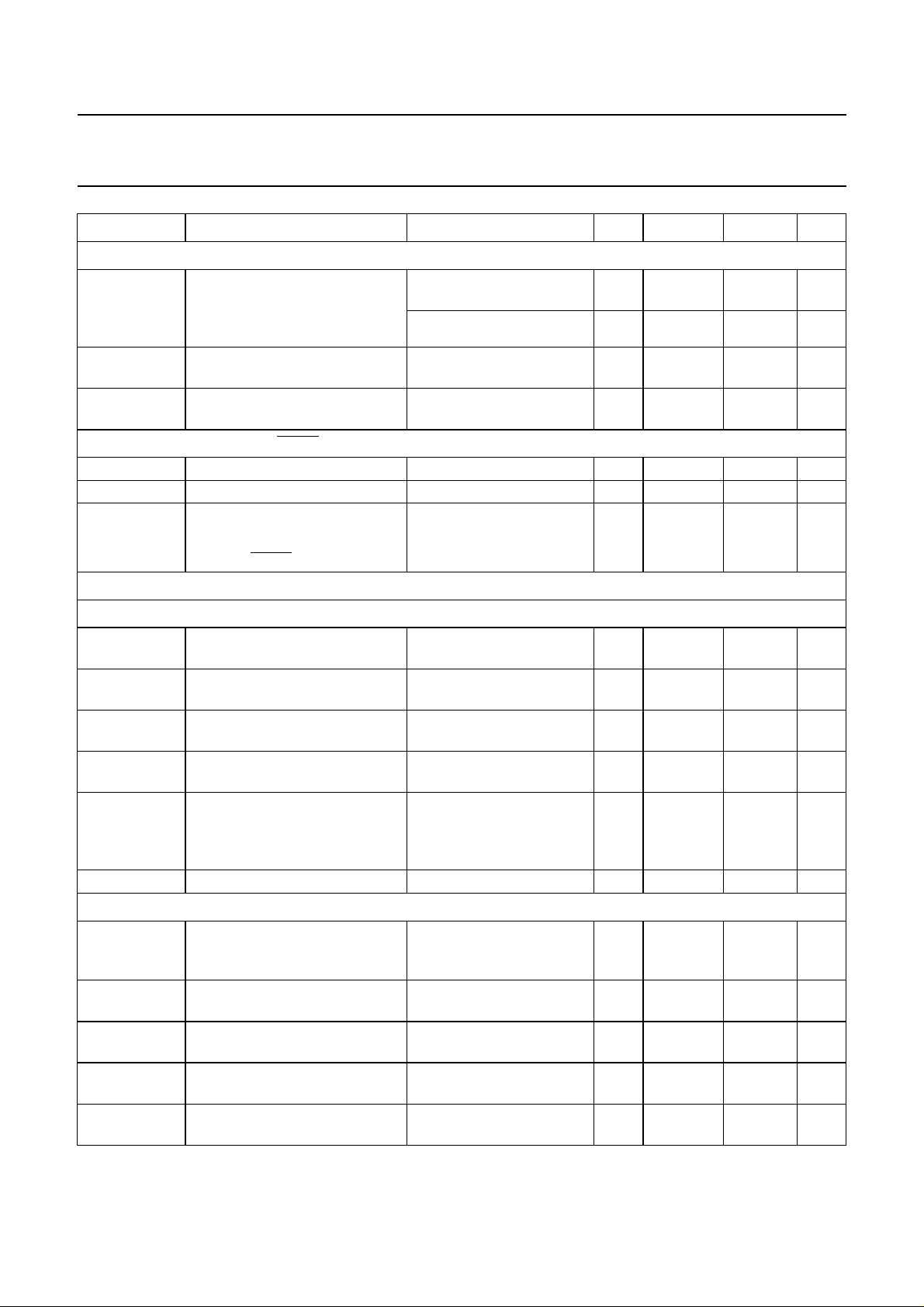
Philips Semiconductors Product specification
Speech and handsfree IC TEA1098
SYMBOL PARAMETER CONDITIONS MIN. TYP. MAX. UNIT
Automatic Gain Control (pin AGC)
∆G
v(trx)
gain control range for transmit
and receive amplifiers affected
by the AGC; with respect to
I
=15mA
line
I
start
highestline currentformaximum
gain
I
stop
lowest line current for maximum
gain
Logic inputs (pins HFC and MUTE)
V
IL
V
IH
I
i
LOW-level input voltage −0.4 − +0.3 V
HIGH-level input voltage 1.8 − VBB+ 0.4 V
input current VBB= 3.0 V
for pin HFC − 36µA
for pin MUTE −−3 −12 µA
Handsfree mode (HFC = HIGH)
I
= 70 mA; G
line
G
v(IR-RECO)
I
= 70 mA for G
line
v(MIC-LN)
v(HFTX-LN)
;
5.45 6.45 7.45 dB
5.8 6.8 7.8 dB
− 23 − mA
− 57 − mA
HF MICROPHONE AMPLIFIER (PINS TXIN, TXOUT AND GATX)
G
v(TXIN-TXOUT)
∆G
v
∆G
v(f)
voltage gain from pin TXIN to
TXOUT
voltage gain adjustment with
R
GATX
gain variation with frequency
V
= 3 mV (RMS);
TXIN
R
= 30.1 kΩ
GATX
f = 300 to 3400 Hz −±0.1 − dB
referenced to 1 kHz
∆G
v(T)
gain variation with temperature
T
= −25 to +75 °C −±0.15 − dB
amb
referenced to 25 °C
V
no(TXOUT)(rms)
noise output voltage at
pin TXOUT; pin TXIN is shorted
psophometrically weighted
(p53 curve)
through 200 Ω in series with
10 µF to GNDTX (RMS value)
∆G
v(mute)
gain reduction if not activated see Table 2 60 80 − dB
HF LOUDSPEAKER AMPLIFIER (PINS HFRX, LSAO, GALS AND VOL)
G
v(HFRX-LSAO)
∆G
v
∆G
v(f)
voltage gain from pin HFRX to
LSAO
voltage gain adjustment with
R
GALS
gain variation with frequency
V
= 30 mV (RMS);
HFRX
R
= 255 kΩ;
GALS
I
=70mA
line
f = 300 to 3400 Hz −±0.3 − dB
referenced to 1 kHz
∆G
v(T)
gain variation with temperature
T
= −25 to +75 °C −±0.3 − dB
amb
referenced to 25 °C
∆G
v(vol)
voltage gain variation related to
∆R
= 1.9 kW
VOL
total attenuation does not
exceed switching range
12.7 15.2 17.7 dB
−15 − +16 dB
−−101 − dBmp
25.5 28 30.5 dB
−28 − +7 dB
−−3 − dB
2001 Aug 24 24
Page 25
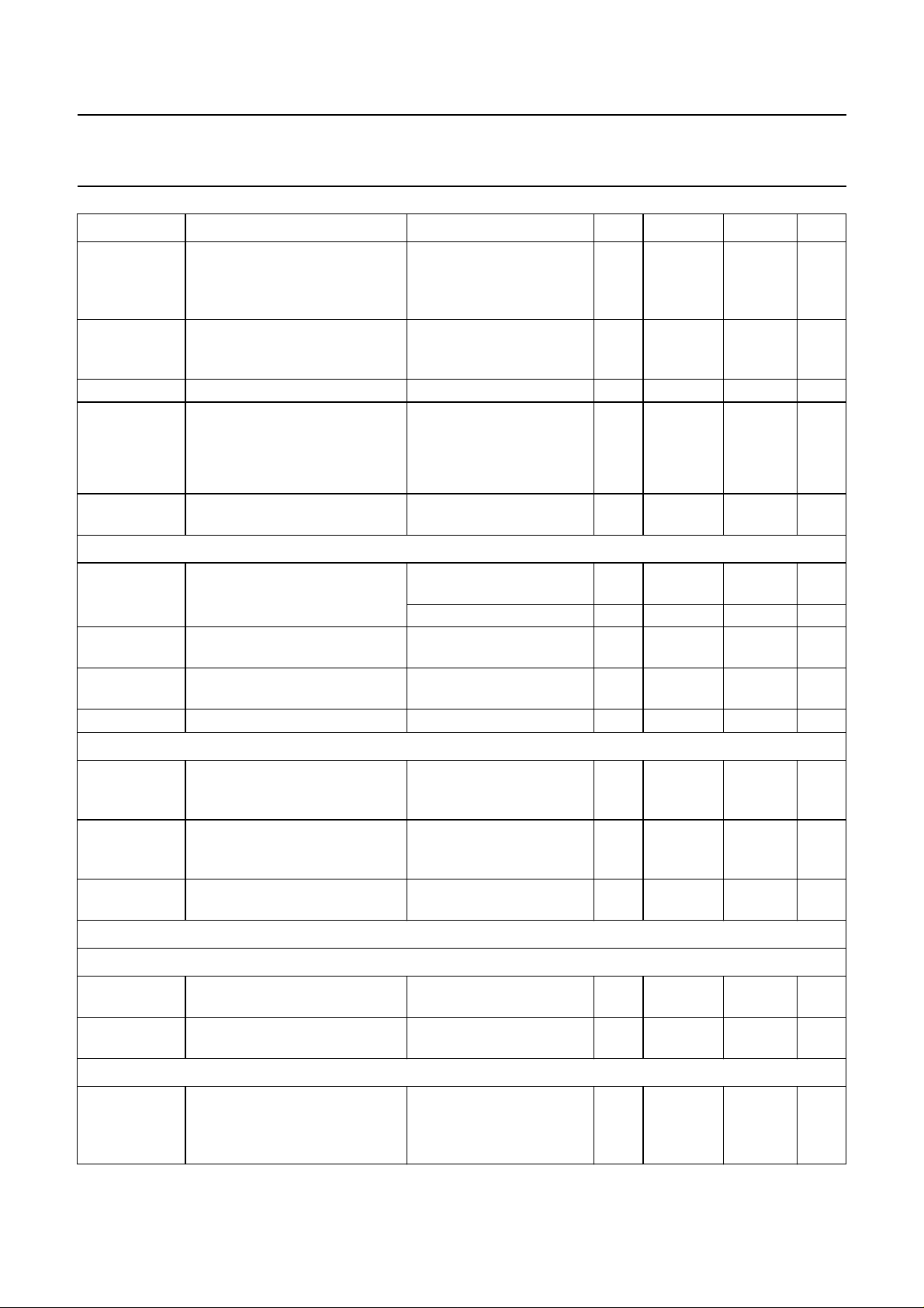
Philips Semiconductors Product specification
Speech and handsfree IC TEA1098
SYMBOL PARAMETER CONDITIONS MIN. TYP. MAX. UNIT
V
HFRX(rms)(max)
V
no(LSAO)(rms)
∆G
v(mute)
V
LSAO(rms)
I
LSAO(max)
DYNAMIC LIMITER (PINS LSAO AND DLC)
t
att
t
rel
THD total harmonic distortion V
V
BB(th)
MUTE RECEIVE (PIN DLC)
V
DLC(th)
I
DLC(th)
∆G
vrx(mute)
TX AND RX ENVELOPE AND NOISE DETECTORS (PINS TSEN, TENV, TNOI, RSEN, RENV AND RNOI)
maximum input voltage at
pin HFRX (RMS value)
I
=70mA;
line
R
GALS
− 580 − mV
=33kΩ; for
THD = 2% in the input
stage
noise output voltage at
pin LSAO; pin HFRX is
psophometrically weighted
(p53 curve)
−−79 − dBVp
open-circuit (RMS value)
gain reduction if not activated see Table 2 60 80 − dB
output voltage (RMS value) IBB= 0 mA; IDD=1mA
I
=18mA − 0.9 − V
line
=30mA − 1.3 − V
I
line
I
>50mA − 1.6 − V
line
maximum output current at
150 300 − mA
pin LSAO (peak value)
attack time V
jumps from
HFRX
−− 5ms
20 mV to 20 mV + 10 dB
V
release time V
jumps below V
BB
jumps from
HFRX
BB(th)
− 1 − ms
− 100 − ms
20 mV + 10 dB to 20 mV
= 20 mV + 10 dB;
HFRX
t>t
att
− 12%
VBB limiter threshold − 2.7 − V
threshold voltage required on
−0.4 − +0.2 V
pin DLC to obtain mute receive
condition
threshold current sourced by
V
= 0.2 V − 100 −µA
DLC
pin DLC in mute receive
condition
voltage gain reduction in mute
V
= 0.2 V 60 80 − dB
DLC
receive condition
Preamplifiers
G
v(TSEN)
voltage gain from
pin TXIN to TSEN
G
v(RSEN)
voltage gain from
pin HFRX to RSEN
Logarithmic compressor and sensitivity adjustment
∆V
det(TSEN)
sensitivity detection on
I
= 0.8 to 160 µA − 18 − mV
TSEN
pin TSEN; voltage change on
pin TENV when doubling the
current from TSEN
2001 Aug 24 25
− 40 − dB
− 0 − dB
Page 26
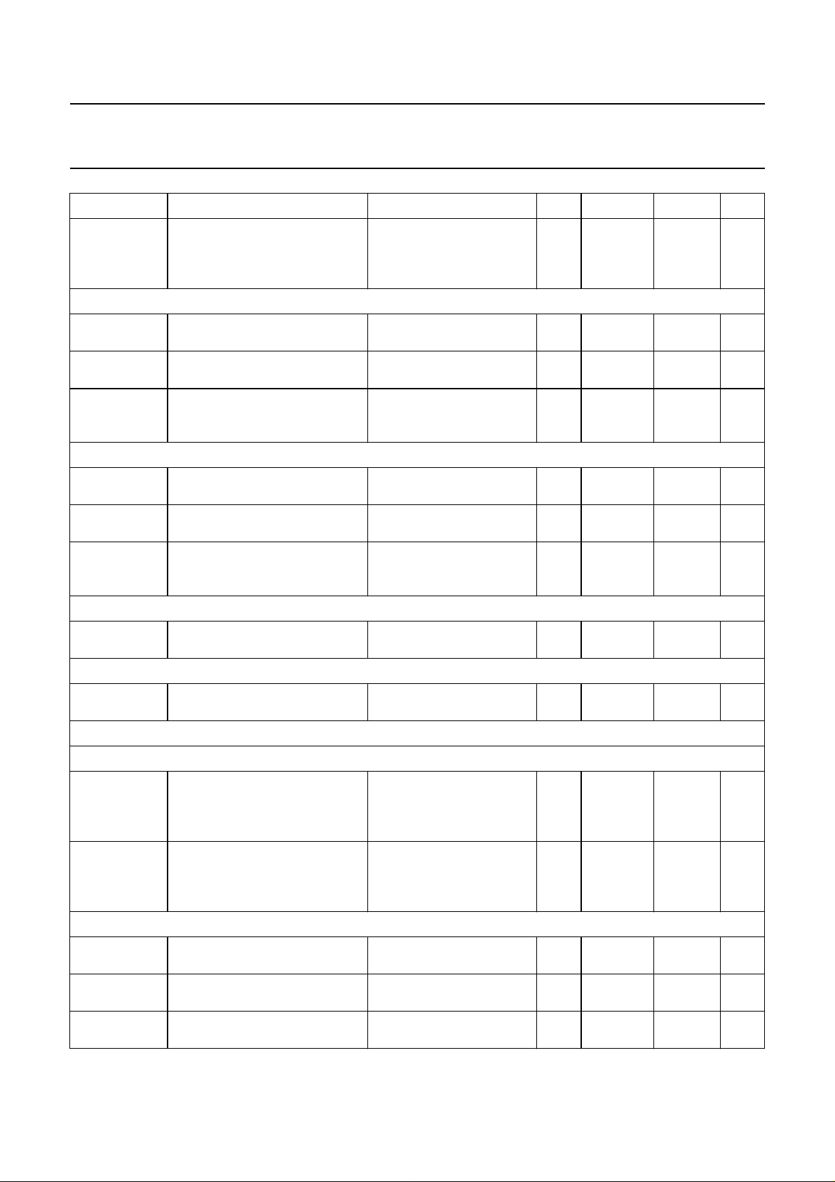
Philips Semiconductors Product specification
Speech and handsfree IC TEA1098
SYMBOL PARAMETER CONDITIONS MIN. TYP. MAX. UNIT
∆V
det(RSEN)
Signal envelope detectors
I
source(ENV)
I
sink(ENV)
∆V
ENV
Noise envelope detectors
I
source(NOI)
I
sink(NOI)
∆V
NOI
DIAL TONE DETECTOR
V
HFRX(th)(rms)
TX LEVEL LIMITER
V
TXIN(th)(rms)
DECISION LOGIC (PINS IDT AND SWT)
sensitivity detection on
pin RSEN; voltage change on
pin RENV when doubling the
current from RSEN
maximum current sourced from
pin TENV or RENV
maximum current sunk by
pin TENV or RENV
voltage difference between
pins RENV and TENV
maximum current sourced from
pin TNOI or RNOI
maximum current sunk by
pin TNOI or RNOI
voltage difference between
pins RNOI and TNOI
threshold level at pin HFRX
(RMS value)
threshold level at pin TXIN
(RMS value)
I
= 0.8 to 160 µA − 18 − mV
RSEN
− 120 −µA
−1.25 −1 −0.75 µA
10 µA is sourced fromboth
−±3 − mV
RSEN and TSEN; signal
detectors tracking; note 1
0.75 1 1.25 µA
−−120 −µA
5 µA is sourced from both
−±3 − mV
RSEN and TSEN; noise
detectors tracking; note 1
R
=10kΩ−25 − mV
RSEN
R
=10kΩ−0.75 − mV
TSEN
Signal recognition
∆V
Srx(th)
threshold voltage between
V
HFRX<VHFRX(th)
pins RENV and RNOI to
switch-over from receive to Idle
mode
∆V
Stx(th)
threshold voltage between
V
TXIN<VTXIN(th)
pins TENV and TNOI to
switch-over from transmit to Idle
mode
Switch-over
I
source(SWT)
current sourced from pin SWT
when switching to receive mode
I
sink(SWT)
current sunk by pin SWT when
switching to transmit mode
I
idle(SWT)
current sourced from pin SWT in
Idle mode
2001 Aug 24 26
; note 2 − 13 − mV
; note 2 − 13 − mV
7.5 10 12.5 µA
−12.5 −10 −7.5 µA
− 0 −µA
Page 27

Philips Semiconductors Product specification
Speech and handsfree IC TEA1098
SYMBOL PARAMETER CONDITIONS MIN. TYP. MAX. UNIT
VOICE SWITCH (PINS STAB AND SWR)
SWRA switching range − 40 − dB
∆SWRA switching range adjustment R
∆G
voltage gain variation from
v
transmit or receive mode to Idle
mode
G
tr
gain tracking (G
vtx+Gvrx
) during
switching, referenced to Idle
mode
Notes
1. Corresponds to ±1 dB tracking.
2. Corresponds to 4.3 dB noise/speech recognition level.
= 365 kΩ−40 − +12 dB
SWR
− 20 − dB
− 0.5 − dB
2001 Aug 24 27
Page 28
This text is here in white to force landscape pages to be rotated correctly when browsing through the pdf in the Acrobat reader.This text is here in
a
_white to force landscape pages to be rotated correctly when browsing through the pdf in the Acrobat reader.This text is here inThis text is here in
white to force landscape pages tobe rotated correctly when browsing through the pdf in the Acrobat reader. white to force landscape pages to be ...
2001 Aug 24 28
Z
exch
600 Ω
C
exch
100 µF
V
HFTX
i = 15 mA
J_line
V
d = 10 V
Z
imp
620 Ω
D
z
C
emc
10 nF
C
imp
100 µF
V
TXIN
V
DTMF
R
TSEN
10 kΩ
C
TSEN
100 nF
V
MIC
C
TXIN
100 nF
C
MICS
4.7 µF
C
HFTX
100 nF
R
GATX
30.1 kΩ
C
DTMF
100 nF
C
TENV
470 nF
V
IR
C
IR
100 nF
R
200 Ω
TXOUT
IR
MICS
MIC+
MIC
MIC−
HFTX
GATX
TXIN
DTMF
TSEN
TENV
TNOI
R
SLPE
20 Ω
SLPE REG AGC LN
17 19 21 18 13 22
20
23
34
33
39
29
30
31
35
8
7
6
16 32 24 25 26 12 27
GND GNDTX
C
TNOI
4.7 µF
ndbook, full pagewidth
C
REG
4.7 µF
STAB
R
STAB
3.65 kΩ
C
VBB
470 µF
V
BB
TEA1098TV
SWR VOL DLC SWT
R
365 kΩ
SWR
R
VOL
0 to
22 kΩ
C
470 nF
DLC
C
V
VDD
47 µF
DD
40
36
37
38
14
15
10
11
28
1
2
5
9
C
SWT
220 nF
PD
HFC
MUTE
QR
GARX
100 kΩ
RECO
HFRX
GALS
LSAO
RSEN
RENV
RNOI
IDT
R
e1
R
IDT
2.2 MΩ
C
100 nF
C
HFRX
100 nF
R
255 kΩ
rxe
GALS
C
GAR
100 pF
C
RNOI
4.7 µF
C
GARS
1 nF
V
HFRX
R
e2
100 kΩ
C
GALS
150 pF
R
RSEN
10 kΩ
C
RENV
470 nF
R
QR
150 Ω
C
4.7 µF
C
LSAO
220 µF
R
LSAO
50 Ω
C
RSEN
100 nF
QR
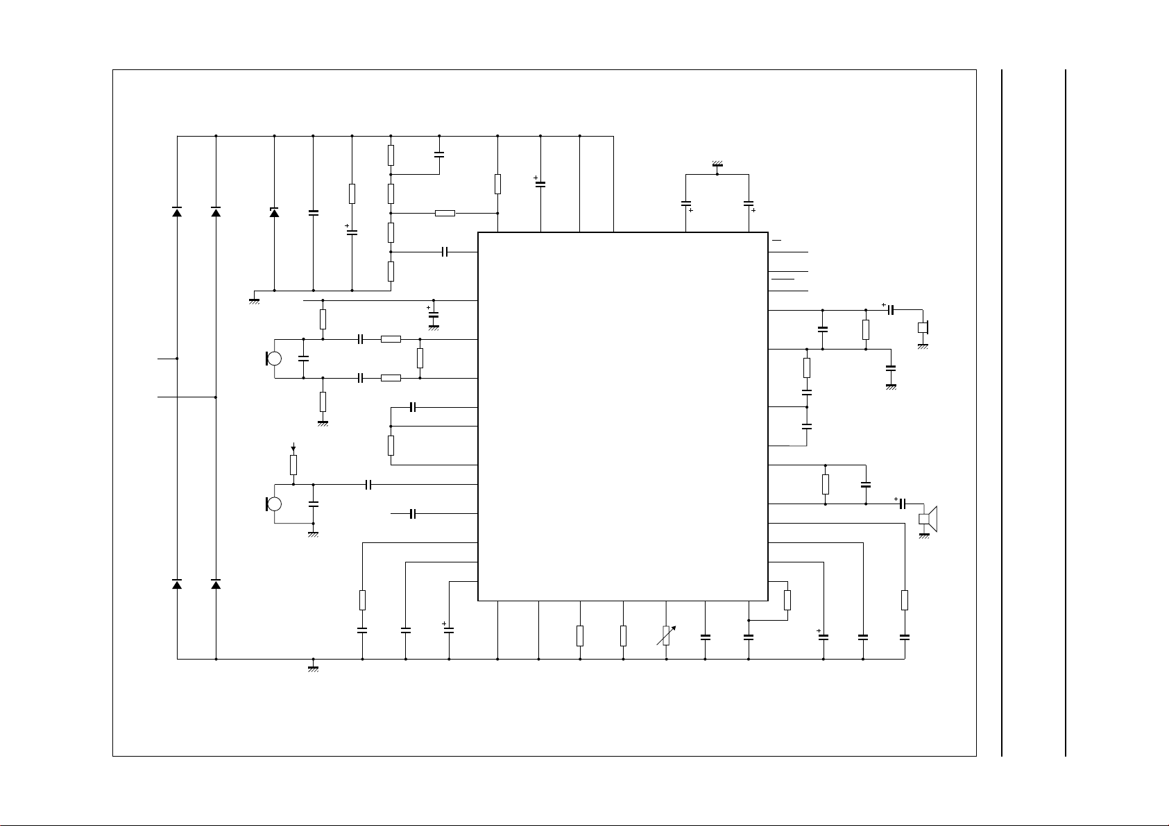
TEST AND APPLICATION INFORMATION
Philips Semiconductors Product specification
Speech and handsfree IC TEA1098
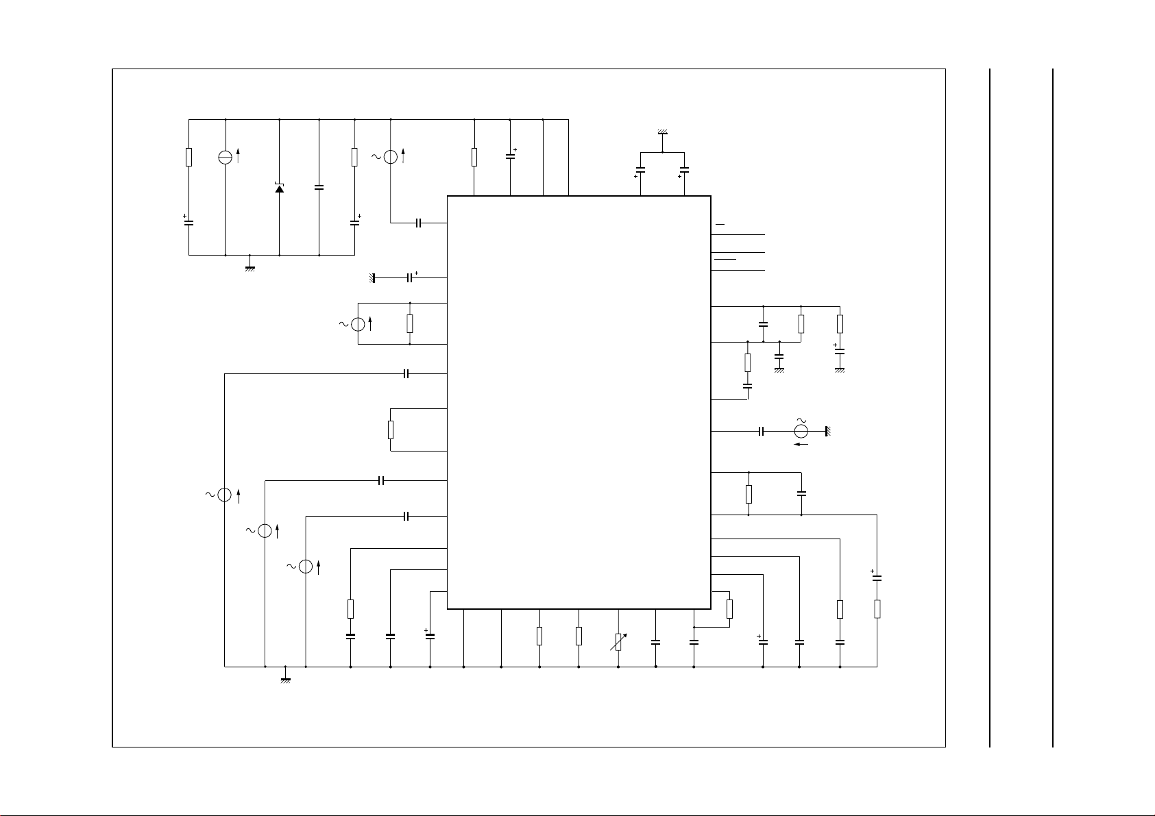
Fig.16 Test configuration.
MGL440
Page 29
This text is here in white to force landscape pages to be rotated correctly when browsing through the pdf in the Acrobat reader.This text is here in
_white to force landscape pages to be rotated correctly when browsing through the pdf in the Acrobat reader.This text is here inThis text is here in
white to force landscape pages tobe rotated correctly when browsing through the pdf in the Acrobat reader. white to force landscape pages to be ...
2001 Aug 24 29
handbook, full pagewidth
Philips Semiconductors Product specification
Speech and handsfree IC TEA1098
A
B
D2 D3
D1 D4
handset
micro
handsfree
micro
D
Vd =
10 V
MICS
from
MICS
HFTX
C
470 nF
R
8.2 kΩ
TENV
R
ast3
392 Ω
C
IR
100 nF
C
10 µF
tx3
C
bal
220 nF
MICS
MICS
MIC+
MIC−
HFTX
TXOUT
GATX
TXIN
DTMF
TSEN
TENV
TNOI
C
4.7 µF
SLPE
C
REG
4.7 µF
TEA1098TV
STAB
R
STAB
3.65 kΩ
SWR VOL DLC SWT
R
R
SWR
365 kΩ
VOL
0 to
22 kΩ
R
20 Ω
SLPE REG AGC LN
17 19 21 18 13 22
IR
20
23
34
33
39
29
30
31
35
8
7
6
16 32 24 25 26 12 27
GND GNDTX
TNOI
C
470 µF
V
BB
VBB
C
DLC
470 nF
C
47 µF
V
DD
1
40
2
36
37
38
5
14
15
10
11
9
28
C
SWT
220 nF
VDD
PD
HFC
MUTE
QR
GARX
RECO
HFRX
GALS
LSAO
RSEN
RENV
RNOI
IDT
R
GALS
255 kΩ
R
IDT
2.2 MΩ
C
100 pF
R
e1
100 kΩ
C
rxe
100 nF
C
HFRX
100 nF
C
150 pF
C
4.7 µF
from
microcontroller
R
GAR
100 kΩ
GALS
C
RNOI
470 nF
C
10 µF
e2
RENV
QR
C
1 nF
C
LSAO
220 µF
GARS
R
RSEN
10 kΩ
C
100 nF
RSEN
R
bal2
820 Ω
R
Z
C
emc
10 nF
MICH
C
MICB
22 nF
R
MICP
1 kΩ
R
MICM
1 kΩ
620 Ω
C
tx2
22 nF
C
tx1
22 nF
C
100 nF
C
22 µF
z
C
33 nF
R
BMICS
2 kΩ
imp
imp
TXIN
R
10 kΩ
C
100 nF
R
15 kΩ
R
15 kΩ
TSEN
TSEN
130 Ω
R
3.92 kΩ
R
130 kΩ
tx2
tx1
bal1
ast2
ast1
C
100 nF
R
GATX
30.1 kΩ
C
DTMF
100 nF
Fig.17 Basic application diagram.
MGL316
Page 30
Philips Semiconductors Product specification
Speech and handsfree IC TEA1098
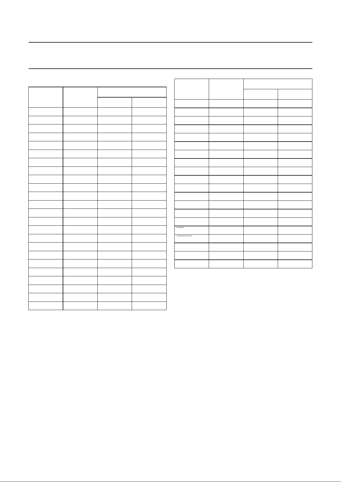
BONDING PAD LOCATIONS FOR TEA1098UH
COORDINATES
SYMBOL PAD
xy
HFRX 1 137.5 3139.2
TNOI 2 137.5 2944.0
TENV 3 137.5 2605.8
TSEN 4 137.5 2375.5
RNOI 5 137.5 2164.5
RSEN 6 137.5 1945.2
RENV 7 137.5 1721.8
DLC 8 137.5 1494.5
V
BB
9 137.5 1050.2
GALS 10 137.5 616.8
LSAO 11 185.2 128.0
n.c. 12 401.2 128.0
GND 13 861.5 128.0
SLPE 14 1125.0 128.0
SLPE 15 1348.2 128.0
LN 16 1537.5 128.0
REG 17 1704.8 128.0
IR 18 1888.8 128.0
AGC 19 2084.0 128.0
V
DD
20 2251.0 128.2
MICS 21 2508.8 127.0
STAB 22 2703.8 128.5
SWR 23 2897.0 128.0
VOL 24 2944.8 343.0
(1)
COORDINATES
(1)
SYMBOL PAD
xy
SWT 25 2944.8 570.0
IDT 26 2945.0 784.0
TXOUT 27 2945.0 973.8
GATX 28 2945.0 1182.0
TXIN 29 2945.0 1390.0
GNDTX 30 2945.0 1581.0
GNDTX 31 2945.0 1747.8
MIC− 32 2945.0 1917.2
MIC+ 33 2945.0 2129.0
DTMF 34 2945.0 2931.0
QR 35 2940.0 3136.8
GARX 36 2651.0 3171.2
RECO 37 2451.0 3171.2
HFTX 38 2170.8 3171.2
HFC 39 1934.2 3171.2
PD 40 1678.8 3171.2
MUTE 41 1425.0 3171.2
n.c. 42 1177.0 3171.2
n.c. 43 942.2 3171.2
n.c. 44 738.5 3171.2
Note
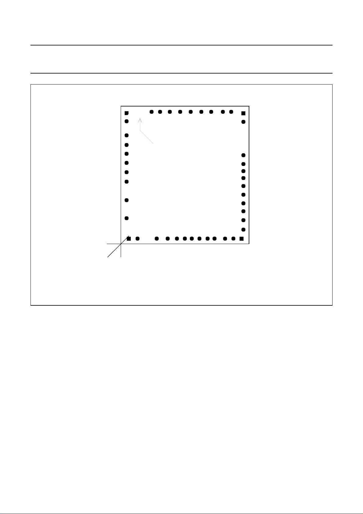
1. Allx/y coordinates(in µm) representthe position ofthe
centre of the pad with respect to the origin (x/y = 0/0)
of the die (see Fig.18).
2001 Aug 24 30
Page 31
Philips Semiconductors Product specification
Speech and handsfree IC TEA1098
44 43 42 41 40 39 38 37 36 35
R9571R
1
2
3
4
5
6
7
8
9
10
0
11
12 13 141516 17 18 19 20 21
0
x
y
die identifier
TEA1098UH/C2
22
FCA200
34
33
32
31
30
29
28
27
26
25
24
23
Pad size: 80 µm2.
Fig.18 TEA1098UH bonding pad locations.
2001 Aug 24 31
Page 32
Philips Semiconductors Product specification
Speech and handsfree IC TEA1098
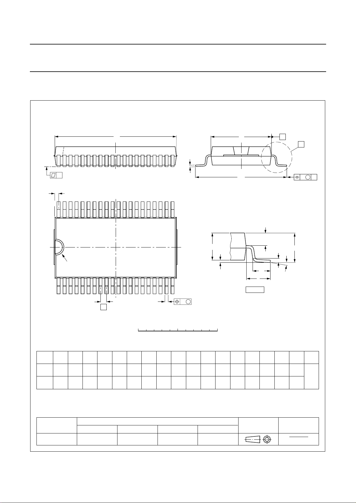
PACKAGE OUTLINE
VSO40: plastic very small outline package; 40 leads
D
y
Z
40
pin 1 index
SOT158-1
E
c
H
E
21
A
2
A
1
L
p
L
A
X
v M
A
Q
(A )
A
3
θ
1
e
0 5 10 mm
DIMENSIONS (inch dimensions are derived from the original mm dimensions)
mm
OUTLINE
VERSION
SOT158-1
A
max.
2.70
0.11
1
0.3
0.1
0.012
0.004
A2A
2.45
2.25
0.096
0.089
IEC JEDEC EIAJ
3
0.25
0.010
b
p
0.42
0.30
0.017
0.012
0.22
0.14
0.0087
0.0055
UNIT A
inches
Notes
1. Plastic or metal protrusions of 0.4 mm maximum per side are not included.
2. Plastic interlead protrusions of 0.25 mm maximum per side are not included.
(1)E(2)
cD
15.6
15.2
0.61
0.60
REFERENCES
20
w M
b
p
scale
eHELLpQywv θ
7.6
0.762 2.25
7.5
0.30
0.03 0.089
0.29
12.3
11.8
0.48
0.46
1.7
1.5
0.067
0.059
detail X
1.15
0.2
1.05
0.045
0.008 0.004
0.041
EUROPEAN
PROJECTION
0.1 0.1
0.004
(1)
Z
0.6
0.3
0.024
0.012
ISSUE DATE
92-11-17
95-01-24
o
7
o
0
2001 Aug 24 32
Page 33

Philips Semiconductors Product specification
Speech and handsfree IC TEA1098
SOLDERING
Introduction to soldering surface mount packages
Thistext gives averybrief insight toa complex technology.
A more in-depth account of soldering ICs can be found in
our
“Data Handbook IC26; Integrated Circuit Packages”
(document order number 9398 652 90011).
There is no soldering method that is ideal for all surface
mount IC packages. Wave soldering can still be used for
certainsurface mount ICs,butit is notsuitablefor fine pitch
SMDs. In these situations reflow soldering is
recommended.
Reflow soldering
Reflow soldering requires solder paste (a suspension of
fine solder particles, flux and binding agent) to be applied
tothe printed-circuitboardby screenprinting,stencilling or
pressure-syringe dispensing before package placement.
Several methods exist for reflowing; for example,
convection or convection/infrared heating in a conveyor
type oven. Throughput times (preheating, soldering and
cooling) vary between 100 and 200 seconds depending
on heating method.
Typical reflow peak temperatures range from
215 to 250 °C. The top-surface temperature of the
packages should preferable be kept below 220 °C for
thick/large packages, and below 235 °C for small/thin
packages.
Wave soldering
Conventional single wave soldering is not recommended
forsurface mount devices(SMDs)or printed-circuit boards
with a high component density, as solder bridging and
non-wetting can present major problems.
To overcome these problems the double-wave soldering
method was specifically developed.
• Use a double-wave soldering method comprising a
turbulent wavewith high upwardpressure followed bya
smooth laminar wave.
• For packages with leads on two sides and a pitch (e):
– larger than or equal to 1.27 mm, the footprint
longitudinal axis is preferred to be parallel to the
transport direction of the printed-circuit board;
– smaller than 1.27 mm, the footprint longitudinal axis
must be parallel to the transport direction of the
printed-circuit board.
The footprint must incorporate solder thieves at the
downstream end.
• Forpackages with leadsonfour sides, thefootprintmust
be placedat a 45° angle to the transport direction of the
printed-circuit board. The footprint must incorporate
solder thieves downstream and at the side corners.
During placement and before soldering, the package must
be fixed with a droplet of adhesive. The adhesive can be
applied by screen printing, pin transfer or syringe
dispensing. The package can be soldered after the
adhesive is cured.
Typical dwell time is 4 seconds at 250 °C.
A mildly-activated flux will eliminate the need for removal
of corrosive residues in most applications.
Manual soldering
Fix the component by first soldering two
diagonally-opposite end leads. Use a low voltage (24 V or
less) soldering iron applied to the flat part of the lead.
Contact time must be limited to 10 seconds at up to
300 °C.
When using a dedicated tool, all other leads can be
soldered in one operation within 2 to 5 seconds between
270 and 320 °C.
If wave soldering is used the following conditions must be
observed for optimal results:
2001 Aug 24 33
Page 34

Philips Semiconductors Product specification
Speech and handsfree IC TEA1098
Suitability of surface mount IC packages for wave and reflow soldering methods
PACKAGE
WAVE REFLOW
(1)
BGA, LFBGA, SQFP, TFBGA not suitable suitable
SOLDERING METHOD
HBCC, HLQFP, HSQFP, HSOP, HTQFP, HTSSOP, SMS not suitable
(3)
PLCC
, SO, SOJ suitable suitable
LQFP, QFP, TQFP not recommended
SSOP, TSSOP, VSO not recommended
(2)
(3)(4)
(5)
suitable
suitable
suitable
Notes
1. All surface mount (SMD) packages are moisture sensitive. Depending upon the moisture content, the maximum
temperature (with respect to time) and body size of the package, there is a risk that internal or external package
cracks may occur due to vaporization of the moisture in them (the so called popcorn effect). For details, refer to the
Drypack information in the
“Data Handbook IC26; Integrated Circuit Packages; Section: Packing Methods”
.
2. These packages are not suitable for wave soldering as a solder joint between the printed-circuit board and heatsink
(at bottom version) can not be achieved, and as solder may stick to the heatsink (on top version).
3. If wave soldering is considered, then the package must be placed at a 45° angle to the solder wave direction.
The package footprint must incorporate solder thieves downstream and at the side corners.
4. Wave soldering is only suitable for LQFP, TQFP and QFP packages with a pitch (e) equal to or larger than 0.8 mm;
it is definitely not suitable for packages with a pitch (e) equal to or smaller than 0.65 mm.
5. Wave soldering is onlysuitable for SSOP and TSSOPpackages with a pitch (e) equal toor larger than 0.65 mm; it is
definitely not suitable for packages with a pitch (e) equal to or smaller than 0.5 mm.
DATA SHEET STATUS
PRODUCT
DATA SHEET STATUS
(1)
STATUS
(2)
DEFINITIONS
Objective data Development This data sheet contains data from the objective specification for product
development. Philips Semiconductors reserves the right to change the
specification in any manner without notice.
Preliminary data Qualification This data sheet contains data from the preliminary specification.
Supplementary data will be published at a later date. Philips
Semiconductors reserves the right to change the specification without
notice, in order to improve the design and supply the best possible
product.
Product data Production This data sheet contains data from the product specification. Philips
Semiconductors reserves the right to make changes at any time in order
to improve the design, manufacturing and supply. Changes will be
communicated according to the Customer Product/Process Change
Notification (CPCN) procedure SNW-SQ-650A.
Notes
1. Please consult the most recently issued data sheet before initiating or completing a design.
2. The product status of the device(s) described in this data sheet may have changed since this data sheet was
published. The latest information is available on the Internet at URL http://www.semiconductors.philips.com.
2001 Aug 24 34
Page 35

Philips Semiconductors Product specification
Speech and handsfree IC TEA1098
DEFINITIONS
Short-form specification The data in a short-form
specification is extracted from a full data sheet with the
same type number and title. For detailed information see
the relevant data sheet or data handbook.
Limiting values definition Limiting valuesgiven are in
accordance with the Absolute Maximum Rating System
(IEC 60134). Stress above one or more of the limiting
values may cause permanent damage to the device.
These are stress ratings only and operation of the device
atthese or atany other conditionsabovethose given inthe
Characteristics sectionsof the specification is not implied.
Exposure to limiting values for extended periods may
affect device reliability.
Application information Applications that are
described herein for any of these products are for
illustrative purposes only. Philips Semiconductors make
norepresentation or warrantythatsuchapplications will be
suitable for the specified use without further testing or
modification.
DISCLAIMERS
Life support applications These products are not
designed for use in life support appliances, devices, or
systems where malfunction of these products can
reasonably be expectedto resultin personalinjury. Philips
Semiconductorscustomers using orsellingtheseproducts
for use in such applications do so at their own risk and
agree to fully indemnify Philips Semiconductors for any
damages resulting from such application.
Right to make changes Philips Semiconductors
reserves the right to make changes, without notice, in the
products, including circuits, standard cells, and/or
software, described or contained herein in order to
improve design and/or performance. Philips
Semiconductors assumes no responsibility or liability for
theuse of anyofthese products, conveysnolicence or title
under any patent, copyright, or mask work right to these
products,and makes norepresentations or warrantiesthat
these products are free from patent, copyright, or mask
work right infringement, unless otherwise specified.
BARE DIE DISCLAIMER
All die are tested and are guaranteed to comply with all
data sheet limits up to the point of wafer sawing for a
periodof ninety(90) days fromthe dateof Philips' delivery.
If there are data sheet limits not guaranteed, these will be
separately indicated in the data sheet. There are no post
packing tests performed on individual die or wafer. Philips
Semiconductorshas nocontrolof thirdpartyprocedures in
the sawing, handling, packing or assembly of the die.
Accordingly, Philips Semiconductors assumes no liability
for device functionality or performance of the die or
systems after third party sawing, handling, packing or
assembly ofthe die. Itis the responsibility of the customer
to test and qualifytheir application in which thedie is used.
2001 Aug 24 35
Page 36

Philips Semiconductors – a w orldwide compan y
Contact information
For additional information please visit http://www.semiconductors.philips.com. Fax: +31 40 27 24825
For sales offices addresses send e-mail to: [email protected].
© Koninklijke Philips Electronics N.V. 2001
All rights are reserved. Reproduction in whole or in part is prohibited without the prior written consent of the copyright owner.
The information presented in this document does not form part of any quotation or contract, is believed to be accurate and reliable and may be changed
without notice. No liability will be accepted by the publisher for any consequence of its use. Publication thereof does not convey nor imply any license
under patent- or other industrial or intellectual property rights.
Printed in The Netherlands 403502/06/pp36 Date of release: 2001 Aug 24 Document order number: 9397 750 08576
SCA73
 Loading...