

Page 1

INTEGRATED CIRCUITS
DATA SH EET
TEA1062; TEA1062A
Low voltage transmission circuits
with dialler interface
Product specification
Supersedes data of 1996 Dec 04
File under Integrated Circuits, IC03
1997 Sep 03
Page 2
Philips Semiconductors Product specification
Low voltage transmission circuits with
dialler interface
FEATURES
• Low DC line voltage; operates down to 1.6 V (excluding
polarity guard)
• Voltage regulator with adjustable static resistance
• Provides a supply for external circuits
• Symmetrical high-impedance inputs (64 kΩ) for
dynamic, magnetic or piezoelectric microphones
• Asymmetrical high-impedance input (32 kΩ) for electret
microphones
• DTMF signal input with confidence tone
• Mute input for pulse or DTMF dialling
– TEA1062: active HIGH (MUTE)
– TEA1062A: active LOW (
• Receiving amplifier for dynamic, magnetic or
piezoelectric earpieces
• Large gain setting ranges on microphone and earpiece
amplifiers
• Line loss compensation (line current dependent) for
microphone and earpiece amplifiers
• Gain control curve adaptable to exchange supply
• DC line voltage adjustment facility.
MUTE)
TEA1062; TEA1062A
GENERAL DESCRIPTION
The TEA1062 and TEA1062A are integrated circuits that
perform all speech and line interface functions required in
fully electronic telephone sets. They perform electronic
switching between dialling and speech. The ICs operate at
line voltage down to 1.6 V DC (with reduced performance)
to facilitate the use of more telephone sets connected in
parallel.
All statements and values refer to all versions unless
otherwise specified.
QUICK REFERENCE DATA
SYMBOL PARAMETER CONDITIONS MIN. TYP. MAX. UNIT
V
I
line
LN
line voltage I
operating line current
= 15 mA 3.55 4.0 4.25 V
line
normal operation 11 − 140 mA
with reduced performance 1 − 11 mA
I
CC
V
CC
G
v
internal supply current VCC= 2.8 V − 0.9 1.35 mA
supply voltage for peripherals I
TEA1062 I
TEA1062A I
=15mA
line
= 1.2 mA; MUTE = HIGH 2.2 2.7 − V
p
I
= 0 mA; MUTE = HIGH − 3.4 − V
p
= 1.2 mA; MUTE = LOW 2.2 2.7 − V
p
= 0 mA; MUTE = LOW − 3.4 − V
I
p
voltage gain
microphone amplifier 44 − 52 dB
receiving amplifier 20 − 31 dB
T
amb
operating ambient temperature −25 − +75 °C
Line loss compensation
∆G
V
R
v
exch
exch
gain control − 5.8 − dB
exchange supply voltage 36 − 60 V
exchange feeding bridge resistance 0.4 − 1kΩ
1997 Sep 03 2
Page 3
Philips Semiconductors Product specification
Low voltage transmission circuits with
TEA1062; TEA1062A
dialler interface
ORDERING INFORMATION
TYPE NUMBER
NAME DESCRIPTION VERSION
TEA1062 DIP16 plastic dual in-line package; 16 leads (300 mil) SOT38-1
TEA1062M1 DIP16 plastic dual in-line package; 16 leads (300 mil) SOT38-4 or
TEA1062A DIP16 plastic dual in-line package; 16 leads (300 mil) SOT38-1
TEA1062AM1 DIP16 plastic dual in-line package; 16 leads (300 mil) SOT38-4 or
TEA1062T SO16 plastic small outline package; 16 leads; body width 3.9 mm SOT109-1
TEA1062A T SO16 plastic small outline package; 16 leads; body width 3.9 mm SOT109-1
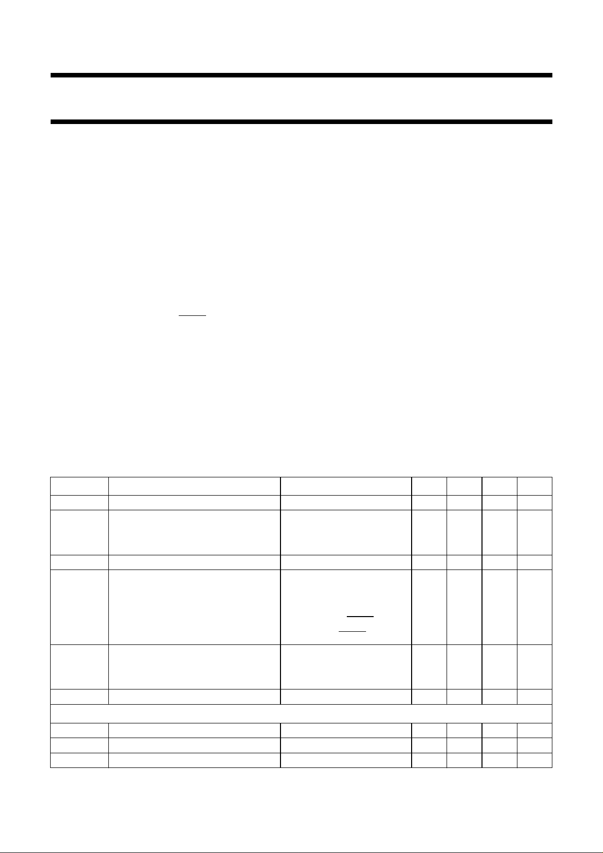
BLOCK DIAGRAM
V
CC
handbook, full pagewidth
10
IR
13
PACKAGE
LN
1
5
SOT38-9
SOT38-9
GAR
(1)
MIC
MIC
DTMF
MUTE
7
6
11
12
SUPPLY AND
REFERENCE
TEA1062A
dB
CONTROL
CURRENT
CURRENT
REFERENCE
91415 8 16
EE
LOW VOLTAGE
CIRCUIT
4
2
3
MBA359 - 1
SLPESTABAGCREGV
QR
GAS1
GAS2
(1) Pin 12 is active HIGH (MUTE) for TEA1062.
Fig.1 Block diagram for TEA1062A.
1997 Sep 03 3
Page 4
Philips Semiconductors Product specification
Low voltage transmission circuits with
dialler interface
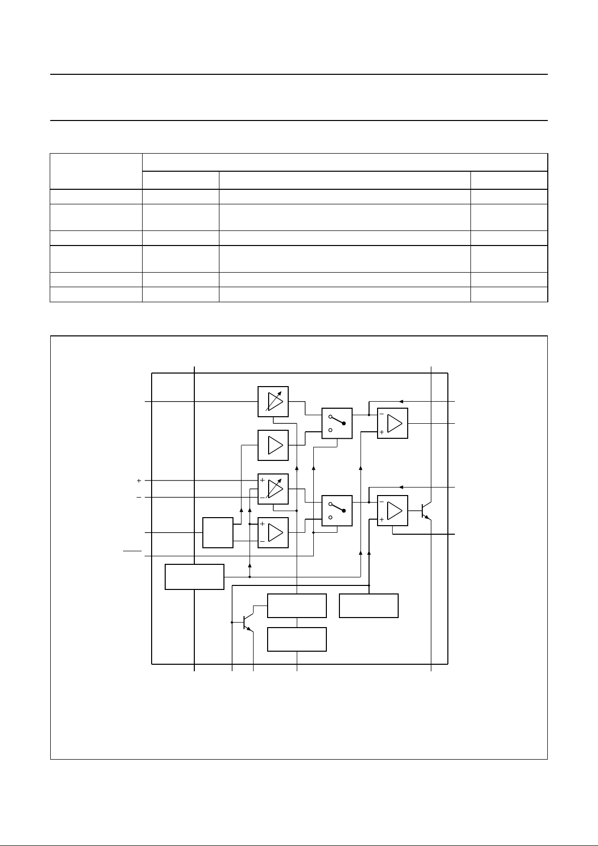
PINNING
SYMBOL PIN DESCRIPTION
LN 1 positive line terminal
GAS1 2 gain adjustment; transmitting
amplifier
GAS2 3 gain adjustment; transmitting
amplifier
QR 4 non-inverting output; receiving
amplifier
GAR 5 gain adjustment; receiving
amplifier
MIC− 6 inverting microphone input
MIC+ 7 non-inverting microphone input
STAB 8 current stabilizer
V
EE
IR 10 receiving amplifier input
DTMF 11 dual-tone multi-frequency input
MUTE 12 mute input (see note 1)
V
CC
REG 14 voltage regulator decoupling
AGC 15 automatic gain control input
SLPE 16 slope (DC resistance) adjustment
9 negative line terminal
13 positive supply decoupling
handbook, halfpage
Fig.2 Pin configuration for TEA1062A.
GAS1
GAS2
QR
GAR
MIC
MIC
STAB
TEA1062; TEA1062A
LN
1
2
3
4
5
6
7
8
TEA1062A
MBA354 - 1
16
15
14
13
12
11
10
9
SLPE
AGC
REG
V
CC
MUTE
DTMF
IR
V
EE
Note
1. Pin 12 is active HIGH (MUTE) for TEA1062.
1997 Sep 03 4
Page 5
Philips Semiconductors Product specification
Low voltage transmission circuits with
dialler interface
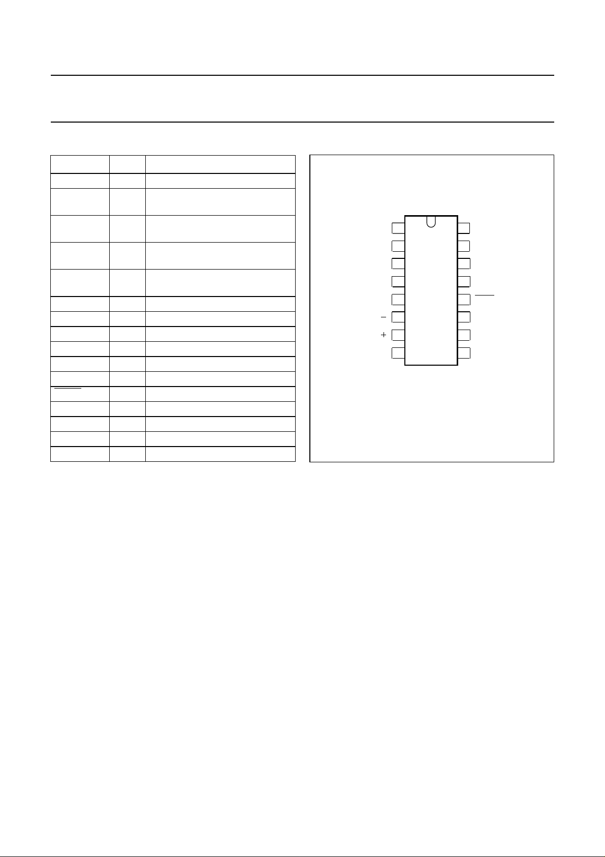
FUNCTIONAL DESCRIPTION
Supplies V
Power for the IC and its peripheral circuits is usually
obtained from the telephone line. The supply voltage is
derived from the line via a dropping resistor and regulated
by the IC. The supply voltage V
supply external circuits e.g. dialling and control circuits.
Decoupling of the supply voltage is performed by a
capacitor between VCC and VEE. The internal voltage
regulator is decoupled by a capacitor between REG and
VEE.
The DC current flowing into the set is determined by the
exchange supply voltage V
resistance R
line R
line
The circuit has an internal current stabilizer operating at a
level determined by a 3.6 kΩ resistor connected between
STAB and VEE (see Fig.9). When the line current (I
more than 0.5 mA greater than the sum of the IC supply
current (ICC) and the current drawn by the peripheral
circuitry connected to VCC (Ip) the excess current is
shunted to VEE via LN.
The regulated voltage on the line terminal (VLN) can be
calculated as:
VLN=V
VLN=V
V
is an internally generated temperature compensated
ref
reference voltage of 3.7 V and R9 is an external resistor
connected between SLPE and VEE.
In normal use the value of R9 would be 20 Ω.
Changing the value of R9 will also affect microphone gain,
DTMF gain, gain control characteristics, sidetone level,
maximum output swing on LN and the DC characteristics
(especially at the lower voltages).
Under normal conditions, when I
the static behaviour of the circuit is that of a 3.7 V regulator
diode with an internal resistance equal to that of R9. In the
audio frequency range the dynamic impedance is largely
determined by R1. Fig.3 shows the equivalent impedance
of the circuit.
, LN, SLPE, REG and STAB
CC
exch
and the DC resistance of the telephone
exch
.
ref+ISLPE
+ {(I
ref
× R9
− ICC− 0.5 × 10⁻³A) − Ip} × R9
line
may also be used to
CC
, the feeding bridge
>> ICC + 0.5 mA + Ip,
SLPE
line
) is
TEA1062; TEA1062A
handbook, halfpage
Leq=C3×R9 × Rp.
Rp= 16.2 kΩ.
At line currents below 9 mA the internal reference voltage
is automatically adjusted to a lower value (typically 1.6 V
at 1 mA). This means that more sets can be operated in
parallel with DC line voltages (excluding the polarity guard)
down to an absolute minimum voltage of 1.6 V. At line
currents below 9 mA the circuit has limited sending and
receiving levels. The internal reference voltage can be
adjusted by means of an external resistor (R
This resistor when connected between LN and REG will
decrease the internal reference voltage and when
connected between REG and SLPE will increase the
internal reference voltage.
Current (Ip) available from VCC for peripheral circuits
depends on the external components used. Fig.10 shows
this current for VCC> 2.2 V. If MUTE is LOW (TEA1062) or
MUTE is HIGH (TEA1062A) when the receiving amplifier
is driven, the available current is further reduced. Current
availability can be increased by connecting the supply IC
(TEA1081) in parallel with R1 as shown in Fig.19 and
Fig.20, or by increasing the DC line voltage by means of
an external resistor (RVA) connected between REG and
SLPE (Fig.18).
LN
L
eq
V
R9
20 Ω
V
EE
ref
R
REG
p
C3
4.7 µF C1100 µF
R1
V
CC
MBA454
Fig.3 Equivalent impedance circuit.
VA
).
1997 Sep 03 5
Page 6

Philips Semiconductors Product specification
Low voltage transmission circuits with
dialler interface
Microphone inputs MIC+ and MIC− and gain pins
GAS1 and GAS2
The circuit has symmetrical microphone inputs. Its input
impedance is 64 kΩ (2 × 32 kΩ) and its voltage gain is
typically 52 dB (when R7 = 68 kΩ, see Figures 14
and 15). Dynamic, magnetic, piezoelectric or electret (with
built-in FET source followers) can be used. Microphone
arrangements are illustrated in Fig.11.
The gain of the microphone amplifier can be adjusted
between 44 dB and 52 dB to suit the sensitivity of the
transducer in use. The gain is proportional to the value of
R7 which is connected between GAS1 and GAS2.
Stability is ensured by two external capacitors, C6
connected between GAS1 and SLPE and C8 connected
between GAS1 and V
may be increased to obtain a first-order low-pass filter.
The value of C8 is 10 times the value of C6. The cut-off
frequency corresponds to the time constant R7 × C6.
. The value of C6 is 100 pF but this
EE
TEA1062; TEA1062A
Receiving amplifier IR, QR and GAR
The receiving amplifier has one input (IR) and a
non-inverting output (QR). Earpiece arrangements are
illustrated in Fig.12. The IR to QR gain is typically 31 dB
(when R4 = 100 kΩ). It can be adjusted between
20 and 31 dB to match the sensitivity of the transducer in
use. The gain is set with the value of R4 which is
connected between GAR and QR. The overall receive
gain, between LN and QR, is calculated by subtracting the
anti-sidetone network attenuation (32 dB) from the
amplifier gain. Two external capacitors, C4 and C7, ensure
stability. C4 is normally 100 pF and C7 is 10 times the
value of C4. The value of C4 may be increased to obtain a
first-order low-pass filter. The cut-off frequency will depend
on the time constant R4 × C4.
The output voltage of the receiving amplifier is specified for
continuous-wave drive. The maximum output voltage will
be higher under speech conditions where the peak to RMS
ratio is higher.
Input MUTE (TEA1062)
When MUTE is HIGH the DTMF input is enabled and the
microphone and receiving amplifier inputs are inhibited.
The reverse is true when MUTE is LOW or open-circuit.
MUTE switching causes only negligible clicking on the line
and earpiece output. If the number of parallel sets in use
causes a drop in line current to below 6 mA the speech
amplifiers remain active independent to the DC level
applied to the MUTE input.
Input MUTE (TEA1062A)
When MUTE is LOW or open-circuit, the DTMF input is
enabled and the microphone and receiving amplifier inputs
are inhibited. The reverse is true when MUTE is HIGH.
MUTE switching causes only negligible clicking on the line
and earpiece output. If the number of parallel sets in use
causes a drop in line current to below 6 mA the DTMF
amplifier becomes active independent to the DC level
applied to the MUTE input.
Dual-tone multi-frequency input DTMF
When the DTMF input is enabled dialling tones may be
sent on to the line. The voltage gain from DTMF to LN is
typically 25.5 dB (when R7 = 68 kΩ) and varies with R7 in
the same way as the microphone gain. The signalling
tones can be heard in the earpiece at a low level
(confidence tone).
Automatic Gain Control input AGC
Automatic line loss compensation is achieved by
connecting a resistor (R6) between AGC and V
The automatic gain control varies the gain of the
microphone amplifier and the receiving amplifier in
accordance with the DC line current. The control range is
5.8 dB which corresponds to a line length of 5 km for a
0.5 mm diameter twisted-pair copper cable with a DC
resistance of 176 Ω/km and average attenuation of
1.2 dB/km). Resistor R6 should be chosen in accordance
with the exchange supply voltage and its feeding bridge
resistance (see Fig.13 and Table 1). The ratio of start and
stop currents of the AGC curve is independent of the value
of R6. If no automatic line-loss compensation is required
the AGC pin may be left open-circuit. The amplifiers, in this
condition, will give their maximum specified gain.
EE
.
1997 Sep 03 6
Page 7

Philips Semiconductors Product specification
Low voltage transmission circuits with
dialler interface
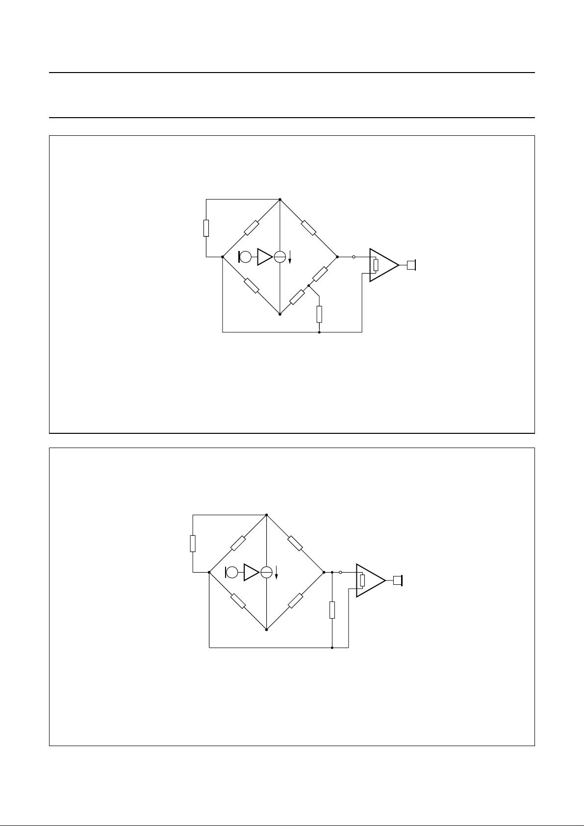
Sidetone suppression
The anti-sidetone network, R1//Z
Z
, (see Fig.4) suppresses the transmitted signal in the
bal
earpiece. Maximum compensation is obtained when the
following conditions are fulfilled:
R9 R2× R1 R3
------------------------ Z
bal
×=
Z
bal
=
R8+
If fixed values are chosen for R1, R2, R3 and R9, then
condition (1) will always be fulfilled when |R8//Z
To obtain optimum sidetone suppression, condition (2) has
to be fulfilled which results in:
R8
Z
bal
Where k is a scale factor;
------- R1
Z
line
kZ
×=×=
line
k
The scale factor k, dependent on the value of R8, is
chosen to meet the following criteria:
• compatibility with a standard capacitor from the E6 or
E12 range for Z
•Z
//R8 << R3 fulfilling condition (a) and thus
bal
bal
ensuring correct anti-sidetone bridge operation
•Z
+ R8 >> R9 to avoid influencing the transmit gain.
bal
In practise Z
varies considerably with the line type and
line
length. The value chosen for Z
an average line length thus giving optimum setting for
short or long lines.
, R2, R3, R8, R9 and
line
×
R8 Z
+
Z
line
-------------------------Z
line
R8
=
------- R1
should therefore be for
bal
bal
------------------------ -
+
R8 Z
bal
R1+
| << R3.
bal
(1)
(2)
TEA1062; TEA1062A
E
XAMPLE
The balance impedance Z
suppression is present can be calculated by:
Suppose Z
= 210 Ω + (1265 Ω//140 nF) representing a
line
5 km line of 0.5 mm diameter, copper, twisted-pair cable
matched to 600 Ω (176 Ω/km; 38 nF/km).
When k = 0.64 then R8 = 390 Ω;
Z
= 130 Ω + (820 Ω//220 nF).
bal
The anti-sidetone network for the TEA1060 family shown
in Fig.4 attenuates the signal received from the line by
32 dB before it enters the receiving amplifier.
The attenuation is almost constant over the whole
audio-frequency range.
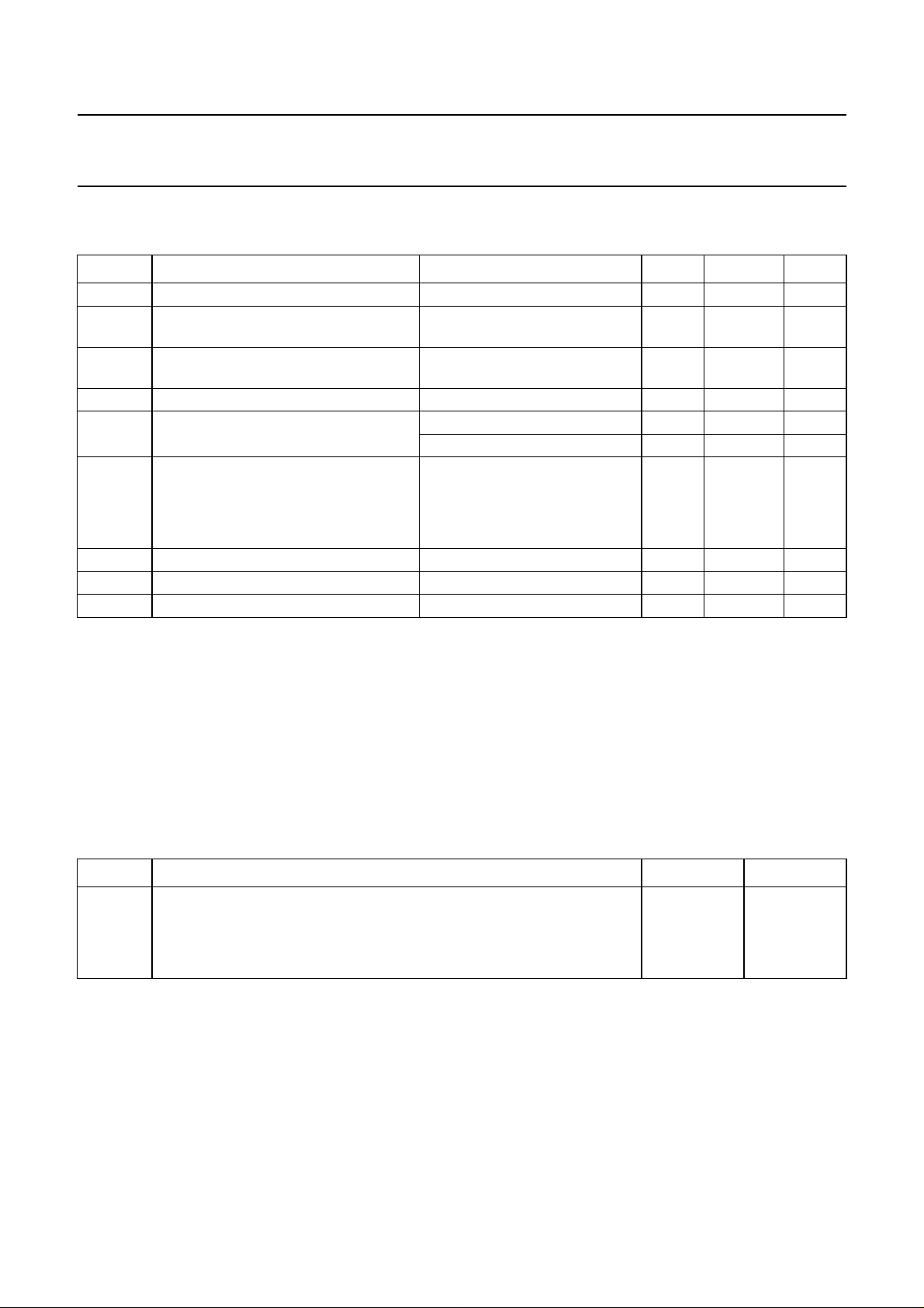
Figure 5 shows a conventional Wheatstone bridge
anti-sidetone circuit that can be used as an alternative.
Both bridge types can be used with either resistive or
complex set impedances. (More information on the
balancing of anti-sidetone bridges can be obtained in our
publication
systems, IC03b”
“Applications Handbook for Wired telecom
, order number 9397 750 00811.)
at which the optimum
bal
1997 Sep 03 7
Page 8
Philips Semiconductors Product specification
Low voltage transmission circuits with
dialler interface
LN
handbook, full pagewidth
Z
line
V
EE
R1 R2
R9
SLPE
TEA1062; TEA1062A
R3
IR
R
t
Z
bal
MSA500 - 1
i
m
R8
ok, full pagewidth
Fig.4 Equivalent circuit of TEA1060 family anti-sidetone bridge.
LN
Z
line
V
EE
R1
R9
SLPE
Z
bal
i
m
R8
IR
R
t
R
A
MSA501 - 1
Fig.5 Equivalent circuit of an anti-sidetone network in a Wheatstone bridge configuration.
1997 Sep 03 8
Page 9
Philips Semiconductors Product specification
Low voltage transmission circuits with
TEA1062; TEA1062A
dialler interface
LIMITING VALUES
In accordance with the Absolute Maximum Rating System (IEC 134).
SYMBOL PARAMETER CONDITIONS MIN. MAX. UNIT
V
LN
V
LN(R)
V
LN(RM)
I
line
V
I
P
tot
T
amb
T
stg
T
j
positive continuous line voltage − 12 V
repetitive line voltage during switch-on
− 13.2 V
or line interruption
repetitive peak line voltage for a 1 ms
pulse per 5 s
R9 = 20 Ω; R10 = 13 Ω;
see Fig.18
− 28 V
line current R9 = 20 Ω; note 1 − 140 mA
input voltage on all other pins positive input voltage − VCC+ 0.7 V
negative input voltage −−0.7 V
total power dissipation R9 = 20 Ω; note 2
TEA1062; TEA1062A − 666 mW
TEA1062M1; TEA1062AM1 − 617 mW
TEA1062T; TEA1062AT − 454 mW
operating ambient temperature −25 +75 °C
storage temperature −40 +125 °C
junction temperature − 125 °C
Notes
1. Mostly dependent on the maximum required T
2. Calculated for the maximum ambient temperature specified (T
and on the voltage between LN and SLPE (see Figs 6, 7 and 8).
amb
=75°C) and a maximum junction temperature of
amb
125 °C.
HANDLING
This device meets class 2 ESD test requirements [Human Body Model (HBM)], in accordance with
“MIL STD 883C - method 3015”
.
THERMAL CHARACTERISTICS
SYMBOL PARAMETER VALUE UNIT
R
th j-a
thermal resistance from junction to ambient in free air
TEA1062; TEA1062A 75 K/W
TEA1062M1; TEA1062AM1 81 K/W
TEA1062T; TEA1062AT (note 1) 110 K/W
Note
1. Mounted on glass epoxy board 28.5 × 19.1 × 1.5 mm.
1997 Sep 03 9
Page 10

Philips Semiconductors Product specification
Low voltage transmission circuits with
dialler interface
150
handbook, halfpage
I
LN
(mA)
130
110
90
70
50
30
212
(1) T
(2) T
(3) T
(4) T
amb
amb
amb
amb
=45°C; P
=55°C; P
=65°C; P
=75°C; P
46810
V
LNVSLPE
= 1068 mW.
tot
= 934 mW.
tot
= 800 mW.
tot
= 666 mW.
tot
MLC200
(1)
(2)
(3)
(4)
(V)
150
handbook, halfpage
I
LN
(mA)
130
110
90
70
50
30
212
(1) T
(2) T
(3) T
(4) T
amb
amb
amb
amb
=45°C; P
=55°C; P
=65°C; P
=75°C; P
TEA1062; TEA1062A
MLC201
(1)
(2)
(3)
(4)
46810
V
LNVSLPE
= 988 mW.
tot
= 864 mW.
tot
= 741 mW.
tot
= 617 mW.
tot
(V)
Fig.6 TEA1062 and TEA1062A safe operating
area.
150
handbook, halfpage
I
LN
(mA)
130
110
90
70
50
30
212
(1) T
amb
(2) T
amb
(3) T
amb
(4) T
amb
46810
=45°C; P
=55°C; P
=65°C; P
=75°C; P
= 727 mW.
tot
= 636 mW.
tot
= 545 mW.
tot
= 454 mW.
tot
(1)
(2)
(3)
(4)
V
LNVSLPE
Fig.7 TEA1062M1 and TEA1062AM1 safe
operating area.
MLC202
(V)
Fig.8 TEA1062T and TEA1062AT safe operating
area.
1997 Sep 03 10
Page 11

Philips Semiconductors Product specification
Low voltage transmission circuits with
TEA1062; TEA1062A
dialler interface
CHARACTERISTICS
I
= 11 to 140 mA; VEE= 0 V; f = 800 Hz; T
line
SYMBOL PARAMETER CONDITIONS MIN. TYP. MAX. UNIT
Supplies LN and V
V
LN
voltage drop over circuit between LN
and V
/∆T variation with temperature I
∆V
LN
V
LN
voltage drop over circuit between LN
(pins 1 and 13)
CC
EE
and VEE with external resistor R
I
CC
V
CC
supply current VCC= 2.8 V − 0.9 1.35 mA
supply voltage available for peripheral
circuitry
TEA1062 I
V
CC
supply voltage available for peripheral
circuitry
TEA1062A I
Microphone inputs MIC− and MIC+ (pins 6 and 7)
Z
input impedance
i
differential between MIC− and MIC+ − 64 − kΩ
single-ended MIC− or MIC+ to V
CMRR common mode rejection ratio − 82 − dB
G
∆G
v
vf
voltage gain MIC+ or MIC− to LN I
gain variation with frequency
referenced to 800 Hz
∆G
vT
gain variation with temperature
referenced to 25 °C
DTMF input (pin 11)
|Z
| input impedance − 20.7 − kΩ
i
G
∆G
v
vf
voltage gain from DTMF to LN I
gain variation with frequency
referenced to 800 Hz
∆G
vT
gain variation with temperature
referenced to 25 °C
=25°C; unless otherwise specified.
amb
MIC inputs open-circuit
I
=1mA − 1.6 − V
line
=4mA − 1.9 − V
I
line
= 15 mA 3.55 4.0 4.25 V
I
line
I
= 100 mA 4.9 5.7 6.5 V
line
I
= 140 mA −−7.5 V
line
=15mA −−0.3 − mV/K
line
I
=15mA
line
VA
R
(LN to REG) = 68 kΩ− 3.5 − V
VA
(REG to SLPE) = 39 kΩ− 4.5 − V
R
VA
I
= 15 mA; MUTE = HIGH
line
= 1.2 mA 2.2 2.7 − V
p
I
=0mA − 3.4 − V
p
I
= 15 mA; MUTE = LOW
line
= 1.2 mA 2.2 2.7 − V
p
I
=0mA − 3.4 − V
p
EE
= 15 mA; R7 = 68 kΩ 50.5 52.0 53.5 dB
line
f = 300 and 3400 Hz −±0.2 − dB
without R6; I
T
= −25 and +75 °C
amb
= 15 mA; R7 = 68 kΩ 24.0 25.5 27.0 dB
line
= 50 mA;
line
f = 300 and 3400 Hz −±0.2 − dB
I
= 50 mA;
line
T
= −25 and +75 °C
amb
− 32 − kΩ
−±0.2 − dB
−±0.2 − dB
1997 Sep 03 11
Page 12

Philips Semiconductors Product specification
Low voltage transmission circuits with
TEA1062; TEA1062A
dialler interface
SYMBOL PARAMETER CONDITIONS MIN. TYP. MAX. UNIT
Gain adjustment inputs GAS1 and GAS2 (pins 2 and 3)
∆G
v
transmitting amplifier gain variation by
adjustment of R7 between
GAS1 and GAS2
Sending amplifier output LN (pin 1)
V
LN(rms)
V
no(rms)
output voltage (RMS value) THD = 10%
I
=4mA − 0.8 − V
line
I
= 15 mA 1.7 2.3 − V
line
noise output voltage (RMS value) I
= 15 mA; R7 = 68 kΩ;
line
200 Ω between MIC− and
MIC+; psophometrically
weighted (P53 curve)
Receiving amplifier input IR (pin 10)
Zi input impedance − 21 − kΩ
Receiving amplifier output QR (pin 4)
Z
output impedance − 4 −Ω
o
G
v
voltage gain from IR to QR I
= 15 mA; RL= 300 Ω
line
(from pin 9 to pin 4)
∆G
vf
gain variation with frequency
f = 300 and 3400 Hz −±0.2 − dB
referenced to 800 Hz
∆G
V
o(rms)
vT
gain variation with temperature
referenced to 25 °C
without R6; I
T
= −25 and +75 °C
amb
= 50 mA;
line
output voltage (RMS value) THD = 2%; sine wave drive;
R4 = 100 kΩ; I
=15mA;
line
Ip=0mA
R
= 150 Ω 0.22 0.33 − V
L
R
= 450 Ω 0.3 0.48 − V
L
V
o(rms)
V
no(rms)
output voltage (RMS value) THD = 10%; R4 = 100 kΩ;
noise output voltage (RMS value) I
RL= 150 Ω; I
= 15 mA; R4 = 100 kΩ;
line
line
=4mA
IR open-circuit
psophometrically weighted
(P53 curve); RL= 300 Ω
−8 − 0dB
−−69 − dBmp
29.5 31 32.5 dB
−±0.2 − dB
− 15 − mV
− 50 −µV
Gain adjustment input GAR (pin 5)
∆G
v
receiving amplifier gain variation by
adjustment of R4 between GAR and QR
Mute input (pin 12)
V
IH
V
IL
I
MUTE
HIGH level input voltage 1.5 − V
LOW level input voltage −−0.3 V
input current − 815µA
1997 Sep 03 12
−11 − 0dB
V
CC
Page 13

Philips Semiconductors Product specification
Low voltage transmission circuits with
TEA1062; TEA1062A
dialler interface
SYMBOL PARAMETER CONDITIONS MIN. TYP. MAX. UNIT
Reduction of gain
∆G
v
G
v
Automatic gain control input AGC (pin 15)
∆G
v
I
lineH
I
lineL
MIC+ or MIC− to LN
TEA1062 MUTE = HIGH − 70 − dB
TEA1062A
MUTE = LOW − 70 − dB
voltage gain from DTMF to QR R4 = 100 kΩ; RL= 300 Ω
TEA1062 MUTE = HIGH −−17 − dB
TEA1062A MUTE = LOW −−17 − dB
controlling the gain from IR to QR
and the gain from MIC+, MIC− to LN
gain control range −−5.8 − dB
R6 = 110 kΩ
(between AGC and VEE)
I
=70mA
line
highest line current for maximum gain − 23 − mA
lowest line current for minimum gain − 61 − mA
handbook, full pagewidth
R
V
exch
exch
R
line R1
TEA1062
TEA1062A
DC
AC
I
line
I
0.5 mA
SLPE
I
SLPE
C3 R5 R9
LN
Fig.9 Supply arrangement.
I
CC
V
CC
I
p
0.5 mA
peripheral
C1
SLPESTABREG
V
EE
circuits
MBA357 - 1
1997 Sep 03 13
Page 14

Philips Semiconductors Product specification
Low voltage transmission circuits with
dialler interface
2.4
handbook, halfpage
(1)
I
p
(mA)
(2)
1.6
0.8
0
012 4
3
TEA1062; TEA1062A
MSA504
VCC(V)
The supply possibilities can be increased by setting the voltage drop over the circuit VLN to a higher value by resistor RVA connected between REG and
SLPE.
> 2.2 V; I
V
CC
(1) Ip= 2.1 mA. Is valid when the receiving amplifier is not driven or when MUTE = HIGH (TEA1062), MUTE = LOW (TEA1062A).
(2) Ip= 1.7 mA. Is valid when MUTE = LOW (TEA1062), MUTE = HIGH (TEA1062A) and the receiving amplifier is driven; V
R
L
= 15 mA at VLN= 4 V; R1 = 620 Ω; R9 = 20 Ω.
line
= 150 Ω.
o(rms)
= 150 mV,
Fig.10 Typical current Ip available from VCC for peripheral circuitry.
1997 Sep 03 14
Page 15

Philips Semiconductors Product specification
Low voltage transmission circuits with
dialler interface
ndbook, full pagewidth
7
MIC
(1)
6
MIC
(a) (b) (c)
(a) Magnetic or dynamic microphone.
(b) Electret microphone.
(c) Piezoelectric microphone.
TEA1062; TEA1062A
13
V
CC
6
MIC
7
MIC
V
EE
9
7
MIC
6
MIC
MSA505
(1) Resistor may be connected to reduce the terminating impedance.
Fig.11 Alternative microphone arrangements.
andbook, full pagewidth
(a) Dynamic earpiece.
(b) Magnetic earpiece.
(c) Piezoelectric earpiece.
4
QR
9
V
EE
(a) (b) (c)
(1)
4
QR
9
V
EE
QR
V
EE
(2)
4
9
MSA506
(1) Resistor may be connected to prevent distortion (inductive load).
(2) Resistor is required to increase the phase margin (capacitive load).
Fig.12 Alternative receiver arrangements.
1997 Sep 03 15
Page 16

Philips Semiconductors Product specification
Low voltage transmission circuits with
dialler interface
handbook, full pagewidth
∆G
(dB)
0
v
2
4
6
78.7 kΩ
110 kΩ 140 kΩ
R6 =
TEA1062; TEA1062A
∞
MSA507 - 1
I (mA)
line
140120100806040200
R9 = 20 Ω.
Fig.13 Variation of gain as a function of line current with R6 as a parameter.
Table 1 Values of resistor R6 for optimum line-loss compensation at various values of exchange supply voltage
(V
) and exchange feeding bridge resistance (R
exch
); R9 = 20 Ω.
exch
R6 (kΩ)
(V)
V
exch
R
= 400 Ω R
exch
= 600 Ω R
exch
= 800 Ω R
exch
exch
= 1000Ω
36 100 78.7 −−
48 140 110 93.1 82
60 −−120 102
1997 Sep 03 16
Page 17

Philips Semiconductors Product specification
Low voltage transmission circuits with
dialler interface
R1
handbook, full pagewidth
100 µF
C1
V
i
10 µF
V
i
10
7
6
11
12
V
IR
MIC
MIC
DTMF
MUTE
V
EE
914 815
C3
4.7
µF
620 Ω
13 1
CC
TEA1062
R6
R5
3.6
kΩ
LN
SLPESTABAGCREG
QR
GAR
GAS1
GAS2
16
R9
20 Ω
TEA1062; TEA1062A
I
line
100 µF
R
L
4
R4
100 kΩ
5
2
R7
68 kΩ
3
600 Ω
C4
100 pF
C7 1 nF
C8
1 nF
C6
100 pF
V
o
MSA508
10 to 140 mA
Voltage gain is defined as Gv=20logVo/Vi.
For measuring gain from MIC+ and MIC− the MUTE input should be LOW or open-circuit.
For measuring the DTMF input, the MUTE input should be HIGH.
Inputs not being tested should be open-circuit.
Fig.14 Test circuit for defining TEA1062 voltage gain of MIC+, MIC− and DTMF inputs.
1997 Sep 03 17
Page 18

Philips Semiconductors Product specification
Low voltage transmission circuits with
dialler interface
R1
handbook, full pagewidth
100 µF
C1
10 µF
10
7
V
i
V
i
6
11
12
IR
MIC
MIC
DTMF
MUTE
V
V
EE
9
C3
4.7
µF
620 Ω
13 1
CC
TEA1062A
14 815
R6
R5
3.6
kΩ
LN
TEA1062; TEA1062A
I
line
100 µF
R
4
QR
R4
100 kΩ
5
GAR
2
GAS1
R7
68 kΩ
3
GAS2
SLPESTABAGCREG
16
R9
20 Ω
600 Ω
C4
100 pF
C7 1 nF
C8
1 nF
C6
100 pF
V
L
o
10 to 140 mA
MBA355
Voltage gain is defined as Gv=20logVo/Vi.
For measuring gain from MIC+ and MIC− the MUTE input should be HIGH.
For measuring the DTMF input, the MUTE input should be LOW or open-circuit.
Inputs not being tested should be open-circuit.
Fig.15 Test circuit for defining TEA1062A voltage gain of MIC+, MIC− and DTMF inputs.
1997 Sep 03 18
Page 19

Philips Semiconductors Product specification
Low voltage transmission circuits with
dialler interface
R1
handbook, full pagewidth
C1
V
i
100 µF
10 µF
10
7
6
11
12
IR
MIC
MIC
DTMF
MUTE
V
EE
V
CC
914 815
C3
4.7
µF
620 Ω
13 1
TEA1062
R6
R5
3.6
kΩ
LN
SLPESTABAGCREG
QR
GAR
GAS1
GAS2
16
R9
20 Ω
TEA1062; TEA1062A
I
line
100 µF
C8
1 nF
600 Ω
10 to 140 mA
MSA509
C2
Z
4
R4
100
kΩ
5
2
R7
3
L
V
o
C4
100 pF
C7 1 nF
C6
100 pF
Voltage gain is defined as Gv=20logVo/Vi.
Fig.16 Test circuit for defining TEA1062 voltage gain of the receiving amplifier.
handbook, full pagewidth
10
7
10 µF
C1
V
i
100 µF
6
11
12
IR
MIC
MIC
DTMF
MUTE
V
EE
R1
620 Ω
13 1
V
CC
TEA1062A
914 815
C3
4.7
µF
R6
R5
3.6
kΩ
LN
SLPESTABAGCREG
QR
GAR
GAS1
GAS2
16
R9
20 Ω
I
line
100 µF
C8
1 nF
600 Ω
10 to 140 mA
MBA356
C2
Z
4
R4
100
kΩ
5
2
R7
3
L
V
o
C4
100 pF
C7 1 nF
C6
100 pF
Voltage gain is defined as Gv=20logVo/Vi.
Fig.17 Test circuit for defining TEA1062A voltage gain of the receiving amplifier.
1997 Sep 03 19
Page 20

Philips Semiconductors Product specification
Low voltage transmission circuits with
dialler interface
APPLICATION INFORMATION
and
from dial
QR
control circuits
12
MUTE
(1)
TEA1062A
GAR
5
7
C1
100
µF
11
DTMF
CC
V
R1
620 Ω
113
LN
IR
10
4
MIC
6
MIC
EEGAS2GAS1
V
SLPE STABAGCREG
9
15 8
314
R7
C6
16 2
R5
3.6
kΩ
R6
C3
16 - 14
(R )
VA
R
100 pF
TEA1062; TEA1062A
MBA358 - 1
4.7
µF
C8
1 nF
R9
20 Ω
, order number 9397 750 00811.
handbook, full pagewidth
C7
1 nF
pF
C4
C5
R2
130 kΩ
BZX79 -
C12
R10
13 Ω
C2
(2x)
BAS11
100 nF
100
R4
R3
3.92
(2x)
BZW14
line
telephone
kΩ
1997 Sep 03 20
R8
390 Ω
bal
Z
(REG to SLPE).
VA
“Applications Handbook for Wired telecom systems, IC03b”
Fig.18 Typical application of TEA1062A, with piezoelectric earpiece and DTMF dialling.
The diode bridge, the Zener diode and R10 limit the current into, and the voltage across, the circuit during line transients.
A different protection arrangement is required for pulse dialling or register recall.
(1) Pin 12 is active HIGH (MUTE) for TEA1062.
The DC line voltage can be set to a higher value by the resistor R
Further application information can be found in our publication
Page 21

Philips Semiconductors Product specification
Low voltage transmission circuits with
dialler interface
handbook, full pagewidth
telephone
cradle
contact
line
BSN254A
LN V
TEA1062
V
EE
620 Ω
R1
CC
DTMF
MUTE
V
DD
TONE
M1 PCD3310
DP/FLO
V
SS
MLC203
TEA1062; TEA1062A
(a) DTMF pulse set with CMOS bilingual dialling circuit PCD3310. The dashed line shows an optional flash (register recall by timed loop break).
Fig.19 Typical simplified application of the TEA1062.
handbook, full pagewidth
telephone
cradle
contact
line
TEA1062A
BSN254A
R1
620 Ω
LN V
V
EE
CC
DTMF
MUTE
V
DD
TONE
M1 PCD3310T
DP/FLO
V
SS
MLC204
(a) DTMF pulse set with CMOS bilingual dialling circuit PCD3310T. The dashed line shows an optional flash (register recall by timed loop break).
Fig.20 Typical simplified application of the TEA1062A.
1997 Sep 03 21
Page 22

Philips Semiconductors Product specification
Low voltage transmission circuits with
dialler interface
PACKAGE OUTLINES
DIP16: plastic dual in-line package; 16 leads (300 mil); long body
D
seating plane
L
Z
16
e
b
b
1
9
A
w M
TEA1062; TEA1062A
SOT38-1
M
E
A
2
A
1
c
(e )
1
M
H
pin 1 index
1
0 5 10 mm
DIMENSIONS (inch dimensions are derived from the original mm dimensions)
A
UNIT
mm
inches
Note
1. Plastic or metal protrusions of 0.25 mm maximum per side are not included.
A
max.
4.7 0.51 3.7
OUTLINE
VERSION
SOT38-1
min.
A
1 2
max.
0.15
IEC JEDEC EIAJ
050G09 MO-001AE
b
1.40
1.14
0.055
0.045
b
1
0.53
0.38
0.021
0.015
cEe M
0.32
0.23
0.013
0.009
REFERENCES
D
21.8
21.4
0.86
0.84
8
scale
(1) (1)
6.48
6.20
0.26
0.24
E
(1)
Z
e
0.30
1
M
L
3.9
3.4
0.15
0.13
E
8.25
7.80
0.32
0.31
EUROPEAN
PROJECTION
9.5
8.3
0.37
0.33
w
H
0.2542.54 7.62
0.010.100.0200.19
ISSUE DATE
92-10-02
95-01-19
max.
2.2
0.087
1997 Sep 03 22
Page 23

Philips Semiconductors Product specification
Low voltage transmission circuits with
dialler interface
DIP16: plastic dual in-line package; 16 leads (300 mil)
D
seating plane
L
Z
16
e
b
TEA1062; TEA1062A
SOT38-4
M
E
A
2
A
A
1
w M
b
1
b
2
9
c
(e )
1
M
H
pin 1 index
1
0 5 10 mm
DIMENSIONS (inch dimensions are derived from the original mm dimensions)
A
A
A
UNIT
max.
mm
inches
Note
1. Plastic or metal protrusions of 0.25 mm maximum per side are not included.
OUTLINE
VERSION
SOT38-4
12
min.
max.
IEC JEDEC EIAJ
b
1.73
1.30
0.068
0.051
b
1
0.53
0.38
0.021
0.015
b
cD E e M
2
0.36
1.25
0.23
0.85
0.014
0.049
0.009
0.033
REFERENCES
8
scale
(1) (1)
19.50
18.55
0.77
0.73
6.48
6.20
0.26
0.24
E
(1)
Z
L
e
1
M
3.60
8.25
3.05
7.80
0.14
0.32
0.12
0.31
EUROPEAN
PROJECTION
E
10.0
0.39
0.33
H
8.3
w
max.
0.2542.54 7.62
ISSUE DATE
0.010.10 0.30
92-11-17
95-01-14
0.764.2 0.51 3.2
0.0300.17 0.020 0.13
1997 Sep 03 23
Page 24

Philips Semiconductors Product specification
Low voltage transmission circuits with
dialler interface
DIP16: plastic dual in-line package; 16 leads (300 mil)
D
seating plane
L
Z
16
e
b
TEA1062; TEA1062A
SOT38-9
M
E
A
2
A
A
1
b
1
w M
b
2
9
c
(e1)
M
H
pin 1 index
1
0 5 10 mm
DIMENSIONS (mm dimensions are derived from the original inch dimensions)
A
min.
A
1
2
max.
b
1.65
0.51
1.40
0.41
0.065
0.020
0.055
0.016
IEC JEDEC EIAJ
b
1
b
2
1.14
0.76
0.045
0.030
REFERENCES
cD E e M
0.36
0.20
0.014
0.008
mm
OUTLINE
VERSION
SOT38-9
A
max.
UNIT
inches
Note
1. Plastic or metal protrusions of 0.01 inches maximum per side are not included.
8
scale
(1) (1)
19.30
18.80
0.76
0.74
6.45
6.24
0.254
0.246
E
(1)
Z
L
e
1
0.150
0.115
M
3.81
8.23
2.92
7.62
0.324
0.300
EUROPEAN
PROJECTION
E
9.40
8.38
0.37
0.33
H
0.2542.54 7.62
ISSUE DATE
w
0.010.10 0.30
97-07-24
max.
0.764.32 0.38 3.56
0.0300.17 0.015 0.14
1997 Sep 03 24
Page 25

Philips Semiconductors Product specification
Low voltage transmission circuits with
dialler interface
SO16: plastic small outline package; 16 leads; body width 3.9 mm
D
c
y
Z
16
9
TEA1062; TEA1062A
SOT109-1
E
H
E
A
X
v M
A
pin 1 index
1
e
0 2.5 5 mm
DIMENSIONS (inch dimensions are derived from the original mm dimensions)
mm
A
max.
1.75
0.069
A1A2A
0.25
1.45
0.10
1.25
0.010
0.057
0.004
0.049
0.25
0.01
b
3
p
0.49
0.25
0.36
0.19
0.0100
0.019
0.0075
0.014
UNIT
inches
Note
1. Plastic or metal protrusions of 0.15 mm maximum per side are not included.
(1)E(1) (1)
cD
10.0
9.8
0.39
0.38
8
b
p
scale
eHELLpQZywv θ
4.0
1.27
3.8
0.16
0.050
0.15
w M
6.2
5.8
0.244
0.228
A
2
1.05
0.041
Q
A
1
detail X
1.0
0.7
0.4
0.6
0.028
0.039
0.020
0.016
(A )
L
p
L
0.25 0.1
0.25
0.01
0.01 0.004
A
3
θ
0.7
0.3
0.028
0.012
o
8
o
0
OUTLINE
VERSION
SOT109-1
IEC JEDEC EIAJ
076E07S MS-012AC
REFERENCES
1997 Sep 03 25
EUROPEAN
PROJECTION
ISSUE DATE
95-01-23
97-05-22
Page 26

Philips Semiconductors Product specification
Low voltage transmission circuits with
dialler interface
SOLDERING
Plastic dual in-line packages
Y DIP OR WAVE
B
The maximum permissible temperature of the solder is
260 °C; this temperature must not be in contact with the
joint for more than 5 s. The total contact time of successive
solder waves must not exceed 5 s.
The device may be mounted up to the seating plane, but
the temperature of the plastic body must not exceed the
specified storage maximum. If the printed-circuit board has
been pre-heated, forced cooling may be necessary
immediately after soldering to keep the temperature within
the permissible limit.
R
EPAIRING SOLDERED JOINTS
Apply the soldering iron below the seating plane (or not
more than 2 mm above it). If its temperature is below
300 °C, it must not be in contact for more than 10 s; if
between 300 and 400 °C, for not more than 5 s.
Plastic small-outline packages
BYWAVE
During placement and before soldering, the component
must be fixed with a droplet of adhesive. After curing the
adhesive, the component can be soldered. The adhesive
can be applied by screen printing, pin transfer or syringe
dispensing.
TEA1062; TEA1062A
Y SOLDER PASTE REFLOW
B
Reflow soldering requires the solder paste (a suspension
of fine solder particles, flux and binding agent) to be
applied to the substrate by screen printing, stencilling or
pressure-syringe dispensing before device placement.
Several techniques exist for reflowing; for example,
thermal conduction by heated belt, infrared, and
vapour-phase reflow. Dwell times vary between 50 and
300 s according to method. Typical reflow temperatures
range from 215 to 250 °C.
Preheating is necessary to dry the paste and evaporate
the binding agent. Preheating duration: 45 min at 45 °C.
R
EPAIRING SOLDERED JOINTS (BY HAND-HELD SOLDERING
IRON OR PULSE
Fix the component by first soldering two, diagonally
opposite, end pins. Apply the heating tool to the flat part of
the pin only. Contact time must be limited to 10 s at up to
300 °C. When using proper tools, all other pins can be
soldered in one operation within 2 to 5 s at between 270
and 320 °C. (Pulse-heated soldering is not recommended
for SO packages.)
For pulse-heated solder tool (resistance) soldering of VSO
packages, solder is applied to the substrate by dipping or
by an extra thick tin/lead plating before package
placement.
-HEATED SOLDER TOOL)
Maximum permissible solder temperature is 260 °C, and
maximum duration of package immersion in solder bath is
10 s, if allowed to cool to less than 150 °C within 6 s.
Typical dwell time is 4 s at 250 °C.
A modified wave soldering technique is recommended
using two solder waves (dual-wave), in which a turbulent
wave with high upward pressure is followed by a smooth
laminar wave. Using a mildly-activated flux eliminates the
need for removal of corrosive residues in most
applications.
1997 Sep 03 26
Page 27

Philips Semiconductors Product specification
Low voltage transmission circuits with
TEA1062; TEA1062A
dialler interface
DEFINITIONS
Data sheet status
Objective specification This data sheet contains target or goal specifications for product development.
Preliminary specification This data sheet contains preliminary data; supplementary data may be published later.
Product specification This data sheet contains final product specifications.
Limiting values
Limiting values given are in accordance with the Absolute Maximum Rating System (IEC 134). Stress above one or
more of the limiting values may cause permanent damage to the device. These are stress ratings only and operation
of the device at these or at any other conditions above those given in the Characteristics sections of the specification
is not implied. Exposure to limiting values for extended periods may affect device reliability.
Application information
Where application information is given, it is advisory and does not form part of the specification.
LIFE SUPPORT APPLICATIONS
These products are not designed for use in life support appliances, devices, or systems where malfunction of these
products can reasonably be expected to result in personal injury. Philips customers using or selling these products for
use in such applications do so at their own risk and agree to fully indemnify Philips for any damages resulting from such
improper use or sale.
1997 Sep 03 27
Page 28

Philips Semiconductors – a worldwide company
Argentina: see South America
Australia: 34 Waterloo Road, NORTH RYDE, NSW 2113,
Tel. +61 2 9805 4455, Fax. +61 2 9805 4466
Austria: Computerstr. 6, A-1101 WIEN, P.O. Box 213,
Tel. +43 1 60 101, Fax. +43 1 60 101 1210
Belarus: Hotel Minsk Business Center, Bld. 3, r. 1211, Volodarski Str. 6,
220050 MINSK, Tel. +375 172 200 733, Fax. +375 172 200 773
Belgium: see The Netherlands
Brazil: seeSouth America
Bulgaria: Philips Bulgaria Ltd., Energoproject, 15thfloor,
51 James Bourchier Blvd., 1407 SOFIA,
Tel. +359 2 689 211, Fax. +359 2 689 102
Canada: PHILIPS SEMICONDUCTORS/COMPONENTS,
Tel. +1 800 234 7381
China/Hong Kong: 501 Hong Kong Industrial Technology Centre,
72 Tat Chee Avenue, Kowloon Tong, HONG KONG,
Tel. +852 2319 7888, Fax. +852 2319 7700
Colombia: see South America
Czech Republic: see Austria
Denmark: Prags Boulevard 80, PB 1919, DK-2300 COPENHAGEN S,
Tel. +45 32 88 2636, Fax. +45 31 57 1949
Finland: Sinikalliontie 3, FIN-02630 ESPOO,
Tel. +358 9 615800, Fax. +358 9 61580/xxx
France: 4 Rue du Port-aux-Vins, BP317, 92156 SURESNES Cedex,
Tel. +33 1 40 99 6161, Fax. +33 1 40 99 6427
Germany: Hammerbrookstraße 69, D-20097 HAMBURG,
Tel. +49 40 23 53 60, Fax. +49 40 23 536 300
Greece: No. 15, 25th March Street, GR 17778 TAVROS/ATHENS,
Tel. +30 1 4894 339/239, Fax. +30 1 4814 240
Hungary: seeAustria
India: Philips INDIA Ltd, Shivsagar Estate, A Block, Dr. Annie Besant Rd.
Worli, MUMBAI 400 018, Tel. +91 22 4938 541, Fax. +91 22 4938 722
Indonesia: see Singapore
Ireland: Newstead, Clonskeagh, DUBLIN 14,
Tel. +353 1 7640 000, Fax. +353 1 7640 200
Israel: RAPAC Electronics, 7 Kehilat Saloniki St, TEL AVIV 61180,
Tel. +972 3 645 0444, Fax. +972 3 649 1007
Italy: PHILIPS SEMICONDUCTORS, Piazza IV Novembre 3,
20124 MILANO, Tel. +39 2 6752 2531, Fax. +39 2 6752 2557
Japan: Philips Bldg 13-37, Kohnan 2-chome, Minato-ku, TOKYO 108,
Tel. +81 3 3740 5130, Fax. +81 3 3740 5077
Korea: Philips House, 260-199 Itaewon-dong, Yongsan-ku, SEOUL,
Tel. +82 2 709 1412, Fax. +82 2 709 1415
Malaysia: No. 76 Jalan Universiti, 46200 PETALING JAYA, SELANGOR,
Tel. +60 3 750 5214, Fax. +60 3 757 4880
Mexico: 5900 Gateway East, Suite 200, EL PASO, TEXAS 79905,
Tel. +9-5 800 234 7381
Middle East: see Italy
Netherlands: Postbus 90050, 5600 PB EINDHOVEN, Bldg. VB,
Tel. +31 40 27 82785, Fax. +31 40 27 88399
New Zealand: 2 Wagener Place, C.P.O. Box 1041, AUCKLAND,
Tel. +64 9 849 4160, Fax. +64 9 849 7811
Norway: Box 1, Manglerud 0612, OSLO,
Tel. +47 22 74 8000, Fax. +47 22 74 8341
Philippines: Philips Semiconductors Philippines Inc.,
106 Valero St. Salcedo Village, P.O. Box 2108 MCC, MAKATI,
Metro MANILA, Tel. +63 2 816 6380, Fax. +63 2 817 3474
Poland: Ul. Lukiska 10, PL 04-123 WARSZAWA,
Tel. +48 22 612 2831, Fax. +48 22 612 2327
Portugal: see Spain
Romania: see Italy
Russia: Philips Russia, Ul. Usatcheva 35A, 119048 MOSCOW,
Tel. +7 095 247 9145, Fax. +7 095 247 9144
Singapore: Lorong 1, Toa Payoh, SINGAPORE 1231,
Tel. +65 350 2538, Fax. +65 251 6500
Slovakia: see Austria
Slovenia: see Italy
South Africa: S.A. PHILIPS Pty Ltd., 195-215 Main Road Martindale,
2092 JOHANNESBURG, P.O. Box 7430 Johannesburg 2000,
Tel. +27 11 470 5911, Fax. +27 11 470 5494
South America: Rua do Rocio 220, 5th floor, Suite 51,
04552-903 São Paulo, SÃO PAULO - SP, Brazil,
Tel. +55 11 821 2333, Fax. +55 11 829 1849
Spain: Balmes 22, 08007 BARCELONA,
Tel. +34 3 301 6312, Fax. +34 3 301 4107
Sweden: Kottbygatan 7, Akalla, S-16485 STOCKHOLM,
Tel. +46 8 632 2000, Fax. +46 8 632 2745
Switzerland: Allmendstrasse 140, CH-8027 ZÜRICH,
Tel. +41 1 488 2686, Fax. +41 1 481 7730
Taiwan: PHILIPS TAIWAN Ltd., 23-30F, 66,
Chung Hsiao West Road, Sec. 1, P.O. Box 22978,
TAIPEI 100, Tel. +886 2 382 4443, Fax. +886 2 382 4444
Thailand: PHILIPS ELECTRONICS (THAILAND) Ltd.,
209/2 Sanpavuth-Bangna Road Prakanong, BANGKOK 10260,
Tel. +66 2 745 4090, Fax. +66 2 398 0793
Turkey: Talatpasa Cad. No. 5, 80640 GÜLTEPE/ISTANBUL,
Tel. +90 212 279 2770, Fax. +90 212 282 6707
Ukraine: PHILIPS UKRAINE, 4 Patrice Lumumba str., Building B, Floor 7,
252042 KIEV, Tel. +380 44 264 2776, Fax. +380 44 268 0461
United Kingdom: Philips Semiconductors Ltd., 276 Bath Road, Hayes,
MIDDLESEX UB3 5BX, Tel. +44 181 730 5000, Fax. +44 181 754 8421
United States: 811 East Arques Avenue, SUNNYVALE, CA 94088-3409,
Tel. +1 800 234 7381
Uruguay: see South America
Vietnam: see Singapore
Yugoslavia: PHILIPS, Trg N. Pasica 5/v, 11000 BEOGRAD,
Tel. +381 11 625 344, Fax.+381 11 635 777
For all other countries apply to: Philips Semiconductors, Marketing & Sales Communications,
Building BE-p, P.O. Box 218, 5600 MD EINDHOVEN, The Netherlands, Fax. +31 40 27 24825
© Philips Electronics N.V. 1996 SCA52
All rights are reserved. Reproduction in whole or in part is prohibited without the prior written consent of the copyright owner.
The information presented in this document does not form part of any quotation or contract, is believed to be accurate and reliable and may be changed
without notice. No liability will be accepted by the publisher for any consequence of its use. Publication thereof does not convey nor imply any license
under patent- or other industrial or intellectual property rights.
Internet: http://www.semiconductors.philips.com
Printed in The Netherlands 417027/1200/05/pp28 Date of release: 1997 Sep 03 Document order number: 9397 750 02819
 Loading...