

Page 1

DATA SH EET
Product specification
Supersedes data of 1996 Sep 05
File under Integrated Circuits, IC03
1998 Mar 02
INTEGRATED CIRCUITS
TEA1204T
High efficiency DC/DC converter
Page 2

1998 Mar 02 2
Philips Semiconductors Product specification
High efficiency DC/DC converter TEA1204T
FEATURES
• Fully integrated DC/DC converter circuit
• Up-or-down conversion, each in 2 different modes
• High efficiency (up to 96%) at high loads
• Output power up to 3.6 W (typ.) continuous, 8 W in GSM
burst mode
• Low quiescent power consumption
• Burst mode input for optimal dynamic response to
switching loads
• True current limit for LiIon battery compatibility
• Up to 100% duty cycle in down mode
• Shut-down function
• 8-pin SO package.
APPLICATIONS
• Cellular and cordless phones PDAs and others
• Supply voltage source for low-voltage chip sets
• Portable computers
• Battery backup supplies
• Cameras.
GENERAL DESCRIPTION
The TEA1204T is a fully integrated DC/DC converter
circuit using the minimum amount of external components.
It is intended to be used to supply electronic circuits with
supply voltages of 3.3, 3.6 or 5.0 V from 2, 3 or 4 NiCd cell
batteries or one LiIon battery at an output power level up
to 3.6 W (typ.) continuously, or 8 W in GSM TDMA (1 : 8)
burst mode. Efficient, compact and dynamic power
conversion is achieved using a novel, digitally controlled
Pulse Width and Frequency Modulation (PWFM) like
control concept, integrated low R
dsON
CMOS power
switches with low parasitic capacitances and synchronous
rectification.
ORDERING INFORMATION
TYPE NUMBER
PACKAGE
NAME DESCRIPTION VERSION
TEA1204T SO8 plastic small outline package; 8 leads; body width 3.9 mm SOT96-1
Page 3
1998 Mar 02 3
Philips Semiconductors Product specification
High efficiency DC/DC converter TEA1204T
QUICK REFERENCE DATA
SYMBOL PARAMETER CONDITIONS MIN. TYP. MAX. UNIT
V
O(up)
output voltage in up mode U/D = LOW, VSEL = LOW 4.75 5.05 5.35 V
U/D = LOW; VSEL = HIGH 3.13 3.34 3.54 V
V
O(down)
output voltage in down mode U/D = HIGH; VSEL = LOW 3.42 3.64 3.85 V
U/D = HIGH; VSEL = HIGH 3.13 3.34 3.54 V
V
start
start-up voltage up mode 1.6 2.0 2.2 V
Efficiency
η efficiency
from 2.4 to 3.3 V 1 mA < I
L
<1.0A 839095%
from 3.6 to 5.0 V 1 mA < I
L
<1.0A 829094%
from 5.0 to 3.6 V 1 mA < I
L
<1.0A 809295%
from 5.0 to 3.3 V 1 mA < I
L
<1.0A 789094%
Current levels
I
q
quiescent current at pin 3 up mode 50 60 70 µA
I
SHDWN
shut-down current − 210µA
I
limN
current limit NFET up mode 2.38 2.80 3.20 A
I
limP
current limit PFET down mode 2.05 2.40 2.75 A
I
LX(max)
maximum continuous current at
pin 5
−−1.0 A
Power MOSFETS
R
dsON(N)
pin-to-pin resistance NFET 0.08 0.12 0.20 Ω
R
dsON(P)
pin-to-pin resistance PFET 0.10 0.16 0.25 Ω
Timing
f
sw
switching frequency 150 200 240 kHz
t
res
response time from standby to P
max
− 25 −µs
Page 4
1998 Mar 02 4
Philips Semiconductors Product specification
High efficiency DC/DC converter TEA1204T
This text is here in white to force landscape pages to be rotated correctly when browsing through the pdf in the Acrobat reader.This text is here in
_white to force landscape pages to be rotated correctly when browsing through the pdf in the Acrobat reader.This text is here inThis text is here in
white to force landscape pages to be rotated correctly when browsing through the pdf in the Acrobat reader. white to force landscape pages to be ...
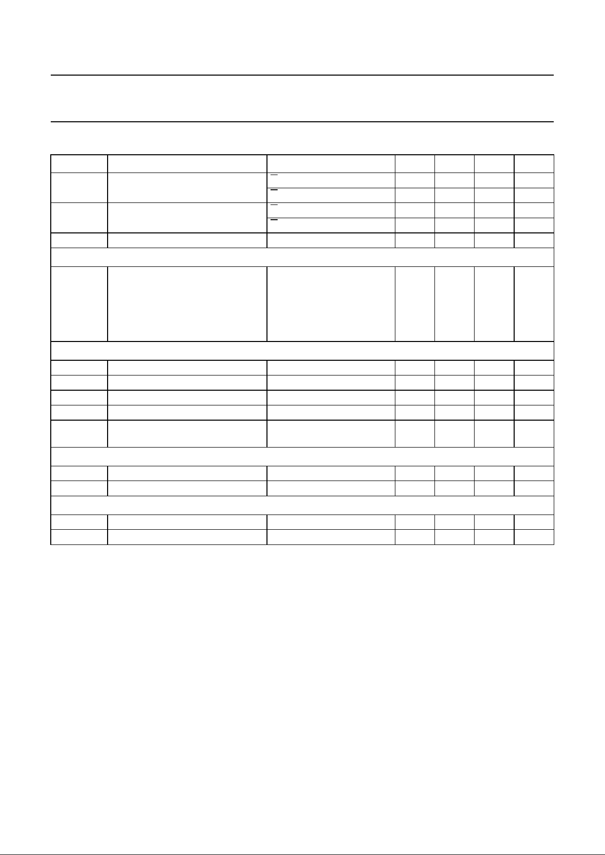
BLOCK DIAGRAM
a
ndbook, full pagewidth
MGK923
CONTROL LOGIC
AND
MODE GEARBOX
ROM
START-UP
CIRCUIT
I/V
CONVERTER
I/V
CONVERTER
TIME
COUNTER
BANDGAP
REFERENCE
20 MHz
OSCILLATOR
TEMPERATURE
PROTECTION
DIGITAL CONTROLLER
sense FET
P-type POWER FET
sense
FET
VSEL
GND
BURST SHDWNU/D
N-type
POWER
FET
LX
UPOUT/DNIN
SENSE
TEA1204T
16278
5
3
4
I
IimP
I
IimN
Fig.1 Block diagram.
Page 5
1998 Mar 02 5
Philips Semiconductors Product specification
High efficiency DC/DC converter TEA1204T
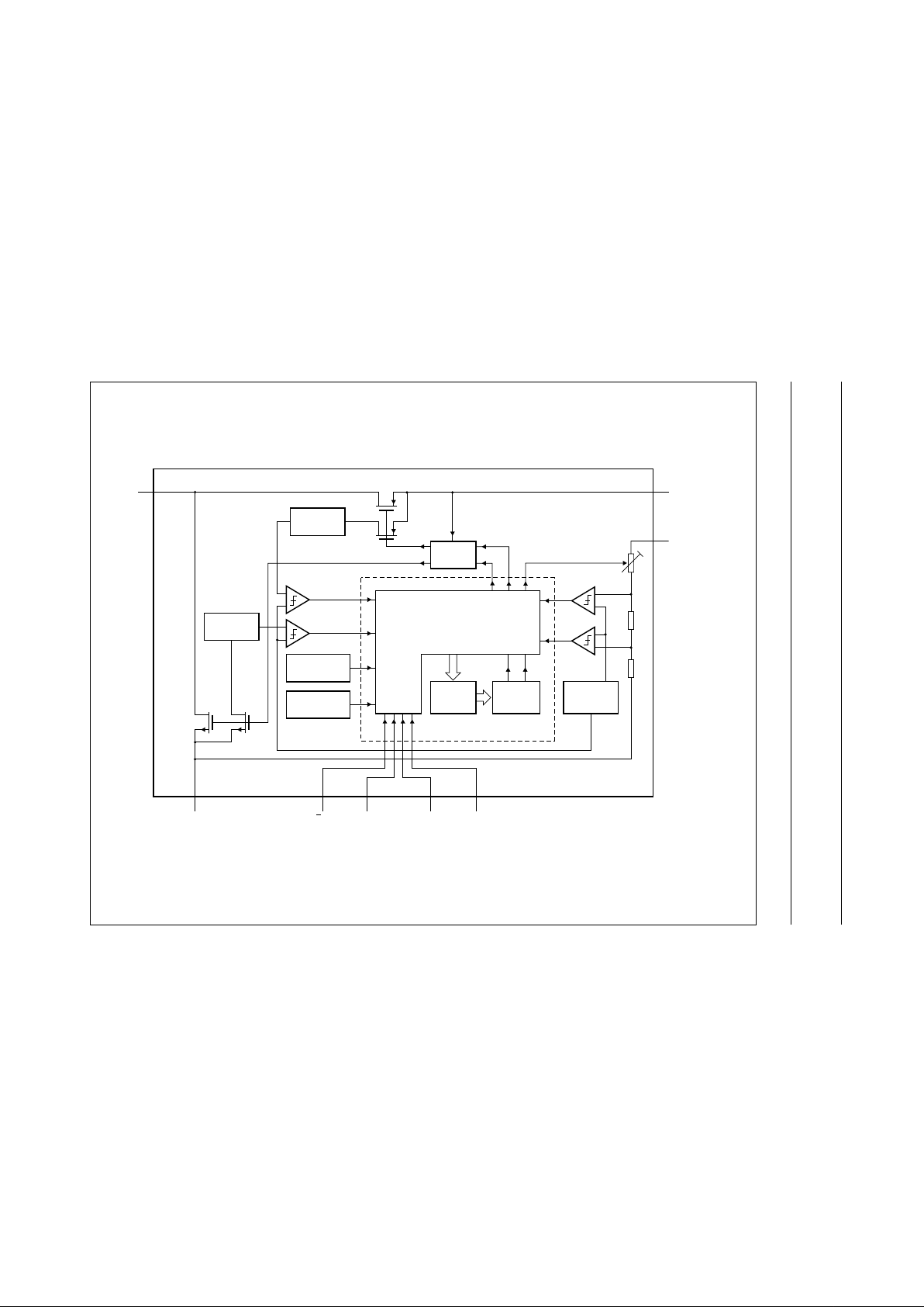
PINNING
SYMBOL PIN DESCRIPTION
U/D 1 conversion mode selection input
VSEL 2 output voltage selection input
UPOUT/DNIN 3 up mode; output voltage/
down mode; input voltage
SENSE 4 output voltage sense input
LX 5 inductor connection
GND 6 ground
BURST 7 burst mode trigger input
SHDWN 8 shut-down input
Fig.2 Pin configuration.
handbook, halfpage
MBH564
1
2
3
4
8
7
6
5
U/D SHDWN
VSEL BURST
UPOUT/DNIN GND
SENSE LX
TEA1204T
FUNCTIONAL DESCRIPTION
Control mechanism
The TEA1204T DC/DC converter is able to operate in
discontinuous or continuous conduction operation.
All switching actions are completely determined by a
digital control circuit which uses the output voltage level as
its control input. This novel digital approach enables the
use of a new pulse width and frequency modulation
scheme, which ensures optimum power efficiency over the
complete range of operation of the converter. The scheme
works as follows. At low output power, a very small current
pulse is generated in the inductor, and the pulse rate
varies with a varying load. When the output voltage drops
below a specific limit, which indicates that the converter’s
current capability is not sufficient, the digital controller
switches to the next state of operation. The peak current in
the inductor is made higher, and the pulse rate can again
vary with a varying load. A third operational state is
available for even higher currents.
When high output power is requested, the device starts
operating in continuous conduction mode. This results in
minimum AC currents in the circuit components and hence
optimum efficiency, cost, and EMC. In this mode, the
output voltage is allowed to vary between two predefined
voltage levels. As long as the output voltage stays within
this so-called window, switching continues in a fixed
pattern. When the output voltage reaches one of the
window borders, the digital controller immediately reacts
by adjusting the pulse width and inserting a current step in
such a way that the output voltage stays within the window
with higher or lower current capability. This approach
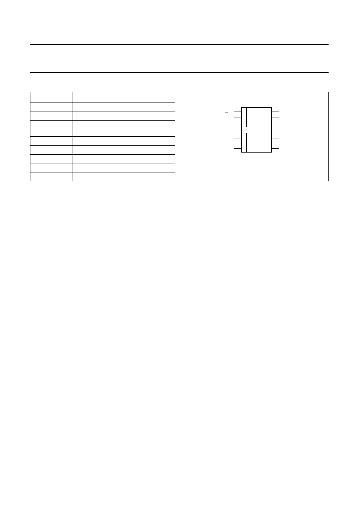
enables very fast reaction to load variations. Figure 3
shows the various coil current waveforms for low and high
current capability in each power conversion mode.
Figure 4 shows the converter’s response to a sudden load
increase. The upper trace shows the output voltage.
The ripple on top of the DC level is a result of the current
in the output capacitor, which changes in sign twice per
cycle, times the capacitor’s internal Equivalent Series
Resistance (ESR). After each ramp-down of the inductor
current, i.e. when the ESR effect increases the output
voltage, the converter determines what to do in the next
cycle. As soon as more load current is taken from the
output the output voltage starts to decay. When the output
voltage becomes lower than the low limit of the window, a
corrective action is taken by a ramp-up of the inductor
current during a much longer time. As a result, the DC
current level is increased and normal continuous
conduction mode can continue. The output voltage
(including ESR effect) is again within the predefined
window.
Figure 5 depicts the spread of the output voltage window.
The absolute value is most dependent on spread, while the
actual window size is not affected. For one specific device,
the output voltage will not vary more than 4%.
Start-up
A possible deadlock situation in boost configuration can
occur after a sequence of disconnecting and reconnecting
the input voltage source. If, after disconnection of the input
source, the output voltage falls below 2.0 V, the device
may not restart properly after reconnection of the input
source, and may take continuous current from the input.
An external circuit to prevent the deadlock situation is
shown in Chapter “Application information”.
Page 6
1998 Mar 02 6
Philips Semiconductors Product specification
High efficiency DC/DC converter TEA1204T
Burst mode trigger input
For burst-mode applications, in which the required output
power periodically changes between two different power
levels, the burst mode trigger feature gains optimal
dynamic response. A digital signal indicating the load
change must be connected to the burst pin. Polarity of the
burst signal is arbitrary. When not used, the burst pin must
be tied to pin 3 or pin 6.
Shut-down
When the shut-down pin is made HIGH, the converter
disables both switches and power consumption is reduced
to a few µA.
Power switches
The power switches in the IC are one N-type and one
P-type MOSFET, having a typical pin-to-pin resistance of
0.12 Ω and 0.16 Ω respectively. The maximum average
current in the switches is 1.0 A.
Temperature protection
At too high device temperature (typical 165 °C), the
converter stops operating. It resumes operation when the
device temperature falls below 165 °C again. As a result,
low-frequent cycling between on and off state will occur.
It should be noted that in the event of device temperatures
around the cut-off limit, the application differs strongly from
maximum specifications.
Current limiters
If the current in one of the power switches exceeds its limit,
current ramping is stopped immediately, and the next
switching phase is entered. Current limitation is required to
enable optimal use of energy in Lithium-Ion batteries, and
to keep power conversion efficient during temporary high
loads. Furthermore, current limitation protects the IC
against overload conditions, inductor saturation, etc.
Behaviour at input voltage exceeding the specified
range
In general, an input voltage exceeding the specified range
is not recommended since instability may occur. There are
two exceptions:
• Upconversion: at an input voltage equal to or higher than
the target output voltage, but up to 6 V, the converter will
stop switching and the external schottky diode will take
over, resulting in V
o
equalling Vi minus the diode voltage
drop.
• Downconversion: when the input voltage is equal to or
lower than the target output voltage, but higher than
2.6 V, the P-type FET will stay conducting resulting in V
o
being equal to Vi minus some resistive voltage drop.
The current limit function remains active.
Fig.3 Coil current waveforms in the various power
modes.
handbook, halfpage
time
low power
mode
medium power
mode 1
medium power
mode 2
low DC current
high DC current
increasing
load
MGK924
Page 7

1998 Mar 02 7
Philips Semiconductors Product specification
High efficiency DC/DC converter TEA1204T
Fig.4 Response to load increase.
ndbook, full pagewidth
MGK925
start corrective action
load increase
high window limit
low window limit
V
o
I
L
time
time
Fig.5 Output voltage window at typical, maximum and minimum specification.
handbook, full pagewidth
MGK926
maximum positive spread
maximum negative spreadtypical situation
lower specification limit
upper specification limit
+3%
+3%
−3%
4%
4%
4%
V
h
V
l
V
h
−3%
V
l
V
h
V
l
5.35
5.15
4.95
4.75
V
o
Page 8

1998 Mar 02 8
Philips Semiconductors Product specification
High efficiency DC/DC converter TEA1204T
LIMITING VALUES
In accordance with the Absolute Maximum Rating System (IEC 134).
Note
1. Human body model: equivalent to discharging a 100 pF capacitor through a 1.5 kΩ series resistor.
THERMAL CHARACTERISTICS
QUALITY SPECIFICATION
In accordance with
“SNW-FQ-611 part E”
. The numbers of the quality specification can be found in the
“Quality
Reference Handbook”
. The handbook can be ordered using the code 9397 750 00192.
CHARACTERISTICS
T
j
= −20 to +80 °C; all voltages with respect to ground; positive currents flow into the IC; unless otherwise specified.
SYMBOL PARAMETER CONDITIONS MIN. MAX. UNIT
V
n
voltage on any pin shut-down mode −0.2 +6.5 V
operational mode −0.2 +5.9 V
T
j
junction temperature −25 +150 °C
T
amb
operating ambient temperature −40 +80 °C
T
stg
storage temperature −65 +125 °C
V
es
electrostatic handling note 1 −3000 +3000 V
SYMBOL PARAMETER CONDITIONS VALUE UNIT
R
th(j-a)
thermal resistance from junction to ambient in free air 150 K/W
SYMBOL PARAMETER CONDITIONS MIN. TYP. MAX. UNIT
Supplies
V
O(up)
output voltage in up mode U/D = LOW, VSEL = LOW 4.75 5.05 5.35 V
U/D = LOW; VSEL = HIGH 3.13 3.34 3.54 V
V
O(down)
output voltage in down mode U/D = HIGH; VSEL = LOW 3.42 3.64 3.85 V
U/D = HIGH; VSEL = HIGH 3.13 3.34 3.54 V
V
start
start-up voltage up mode 1.6 2.0 2.2 V
Efficiency
η efficiency
from 2.4 to 3.3 V 1 mA < I
L
<1.0A 839095%
from 3.6 to 5.0 V 1 mA < I
L
<1.0A 829094%
from 5.0 to 3.6 V 1 mA < I
L
<1.0A 809295%
from 5.0 to 3.3 V 1 mA < I
L
<1.0A 789094%
Page 9

1998 Mar 02 9
Philips Semiconductors Product specification
High efficiency DC/DC converter TEA1204T
Notes
1. The average inductor current during current limit also depends on inductance value and resistive losses in all
components in the power path. In normal applications, the average current will be limited to 2.3 A (typ.), with limits
scaled down to minimum 2.07 A and maximum 2.53 A.
2. V3 is the voltage at pin 3 (UPOUT/DNIN).
3. If the applied high level is less than V3− 1 V, the quiescent current level of the device will increase. The maximum
increase is 300 µA in the event that pin 2 is at 2.0 V.
Current levels
I
q
quiescent current at pin 3 up mode 50 60 70 µA
I
SHDWN
shut-down current − 210µA
I
limN
current limit NFET up mode; note 1 2.38 2.80 3.20 A
I
limP
current limit PFET down mode; note 1 2.05 2.40 2.75 A
I
LX(max)
maximum continuous current
at pin 5
−−1.0 A
Power MOSFETS
R
dsON(N)
pin-to-pin resistance NFET 0.08 0.12 0.20 Ω
R
dsON(P)
pin-to-pin resistance PFET 0.10 0.16 0.25 Ω
Timing
f
sw
switching frequency 150 200 240 kHz
t
res
response time from standby to
P
max
− 25 −µs
T emperature
T
amb
operating ambient temperature −20 +25 +80 °C
T
max
internal cut-off temperature 150 165 180 °C
Digital levels
V
lL
LOW-level input voltage pins
1, 2, 7 and 8
0 − 0.4 V
V
IH
HIGH-level input voltage pin 1 note 2 V3− 0.4 − V3+ 0.3 V
V
IH
HIGH-level input voltage pin 2 notes 2 and 3 2.0 − V3+ 0.3 V
V
IH
HIGH-level input voltage
pins 7 and 8
notes 2 and 3 2.9 − V3+ 0.3 V
Sense pin resistance
R
SENSE
SENSE pin resistance to GND up or down to 3.3 V mode 437.2 546.5 655.8 kΩ
down to 3.6 V mode 476.8 596.0 715.2 kΩ
up to 5.0 V mode 662.2 827.8 993.4 kΩ
SYMBOL PARAMETER CONDITIONS MIN. TYP. MAX. UNIT
Page 10

1998 Mar 02 10
Philips Semiconductors Product specification
High efficiency DC/DC converter TEA1204T
APPLICATION INFORMATION
Fig.6 Complete application for upconversion.
handbook, full pagewidth
MGK928
C1
L1
C2
D1
SENSE
UPOUT/DNIN
V
O
TEA1204T
LX
GND U/D VSEL BURST SHDWN
V
I
Fig.7 Complete application for downconversion.
handbook, full pagewidth
GND U/D VSEL BURST SHDWN
MGK929
C1
C2
D1
LX
SENSE
L1
V
O
TEA1204T
UPOUT/DNIN
V
I
Page 11

1998 Mar 02 11
Philips Semiconductors Product specification
High efficiency DC/DC converter TEA1204T
A typical component choice for an upconverter from
3 NiCd cells or one LiIon cell to 5.0 V in a GSM handset
(peak power 7.5 W, peak current 2.7 A) is:
• L1; L = 10 µH; I
sat
>2.3 A; low DC resistance, e.g.
Coilcraft DO3308-103
• C1; C = 100 µF; low ESR capacitor; necessity depends
on type of input voltage source
• C2; C = 330 µF; ESR = 0.1 Ω; e.g. Sprague 595D series
• D1; medium power Schottky diode; e.g. Philips
PRLL5819.
For lower power applications, the I
sat
and RDC values of
the inductor can be scaled back by the scaling factor of the
output current from the values above. The same holds for
the ESR value of the output capacitor. A further
improvement is increase of inductance and decrease of
output capacitance.
An additional circuit to prevent start-up deadlock in
upconversion is shown in Fig.8. The function of TR1, R1
and R2 is to put the converter into shut-down mode when
the input source is suddenly disconnected. The circuit
operates as follows. When VI is present, TR1 conducts
and the SHDWN pin is kept LOW. As soon as VI falls below
1 V, TR1 no longer conducts and the device is put into
shut-down before VO falls below 2 V. In the event that a
signal is available which indicates the presence of the
input voltage source, this signal should be applied to the
SHDWN pin. TR1, R1 and R2 should be omitted in that
case.
More application information can be found in the
associated application note.
Fig.8 External deadlock prevention circuit.
handbook, halfpage
MGK930
SHDWN
TR1
R1
1 MΩ
R2
2.7 MΩ
V
O
V
I
Page 12

1998 Mar 02 12
Philips Semiconductors Product specification
High efficiency DC/DC converter TEA1204T
Fig.9 Efficiency as a function of load current (2.4 to 3.3 V).
Using a Coilcraft DO3316P 10 µH inductor and a Sprague 595D 330 µF capacitor.
The dashed line represents the Pulse Frequency Modulation (PFM) and the full line the Pulse Width Modulation (PWM).
handbook, full pagewidth
40
100
MGM601
50
60
70
90
80
10
−1
110 10
3
10
2
IL (mA)
efficiency
(%)
Fig.10 Efficiency as a function of load current (3.6 to 5.0 V).
Using a Coilcraft DO3316P 10 µH inductor and a Sprague 595D 330 µF capacitor.
The dashed line represents the Pulse Frequency Modulation (PFM) and the full line the Pulse Width Modulation (PWM).
handbook, full pagewidth
40
100
MGM602
50
60
70
90
80
10
−1
110 10
3
10
2
IL (mA)
efficiency
(%)
Page 13

1998 Mar 02 13
Philips Semiconductors Product specification
High efficiency DC/DC converter TEA1204T
Fig.11 Efficiency as a function of load current (5.0 to 3.3 V).
Using a Coilcraft DO3316P 10 µH inductor and a Sprague 595D 330 µF capacitor.
The dashed line represents the Pulse Frequency Modulation (PFM) and the full line the Pulse Width Modulation (PWM).
handbook, full pagewidth
40
100
MGM603
50
60
70
90
80
10
−1
110 10
3
10
2
IL (mA)
efficiency
(%)
Fig.12 Efficiency as a function of load current (5.0 to 3.6 V).
Using a Coilcraft DO3316P 10 µH inductor and a Sprague 595D 330 µF capacitor.
The dashed line represents the Pulse Frequency Modulation (PFM) and the full line the Pulse Width Modulation (PWM).
handbook, full pagewidth
40
100
MGM604
50
60
70
90
80
10
−1
110 10
3
10
2
IL (mA)
efficiency
(%)
Page 14

1998 Mar 02 14
Philips Semiconductors Product specification
High efficiency DC/DC converter TEA1204T
PACKAGE OUTLINE
UNIT
A
max.
A
1
A
2
A3b
p
cD
(1)E(2)
(1)
eHELLpQZywv θ
REFERENCES
OUTLINE
VERSION
EUROPEAN
PROJECTION
ISSUE DATE
IEC JEDEC EIAJ
mm
inches
1.75
0.25
0.10
1.45
1.25
0.25
0.49
0.36
0.25
0.19
5.0
4.8
4.0
3.8
1.27
6.2
5.8
1.05
0.7
0.6
0.7
0.3
8
0
o
o
0.25 0.10.25
DIMENSIONS (inch dimensions are derived from the original mm dimensions)
Notes
1. Plastic or metal protrusions of 0.15 mm maximum per side are not included.
2. Plastic or metal protrusions of 0.25 mm maximum per side are not included.
1.0
0.4
SOT96-1
X
w M
θ
A
A
1
A
2
b
p
D
H
E
L
p
Q
detail X
E
Z
e
c
L
v M
A
(A )
3
A
4
5
pin 1 index
1
8
y
076E03S MS-012AA
0.069
0.010
0.004
0.057
0.049
0.01
0.019
0.014
0.0100
0.0075
0.20
0.19
0.16
0.15
0.050
0.244
0.228
0.028
0.024
0.028
0.012
0.010.010.041 0.004
0.039
0.016
0 2.5 5 mm
scale
SO8: plastic small outline package; 8 leads; body width 3.9 mm
SOT96-1
95-02-04
97-05-22
Page 15

1998 Mar 02 15
Philips Semiconductors Product specification
High efficiency DC/DC converter TEA1204T
SOLDERING
Introduction
There is no soldering method that is ideal for all IC
packages. Wave soldering is often preferred when
through-hole and surface mounted components are mixed
on one printed-circuit board. However, wave soldering is
not always suitable for surface mounted ICs, or for
printed-circuits with high population densities. In these
situations reflow soldering is often used.
This text gives a very brief insight to a complex technology.
A more in-depth account of soldering ICs can be found in
our
“IC Package Databook”
(order code 9398 652 90011).
Reflow soldering
Reflow soldering techniques are suitable for all SO
packages.
Reflow soldering requires solder paste (a suspension of
fine solder particles, flux and binding agent) to be applied
to the printed-circuit board by screen printing, stencilling or
pressure-syringe dispensing before package placement.
Several techniques exist for reflowing; for example,
thermal conduction by heated belt. Dwell times vary
between 50 and 300 seconds depending on heating
method. Typical reflow temperatures range from
215 to 250 °C.
Preheating is necessary to dry the paste and evaporate
the binding agent. Preheating duration: 45 minutes at
45 °C.
Wave soldering
Wave soldering techniques can be used for all SO
packages if the following conditions are observed:
• A double-wave (a turbulent wave with high upward
pressure followed by a smooth laminar wave) soldering
technique should be used.
• The longitudinal axis of the package footprint must be
parallel to the solder flow.
• The package footprint must incorporate solder thieves at
the downstream end.
During placement and before soldering, the package must
be fixed with a droplet of adhesive. The adhesive can be
applied by screen printing, pin transfer or syringe
dispensing. The package can be soldered after the
adhesive is cured.
Maximum permissible solder temperature is 260 °C, and
maximum duration of package immersion in solder is
10 seconds, if cooled to less than 150 °C within
6 seconds. Typical dwell time is 4 seconds at 250 °C.
A mildly-activated flux will eliminate the need for removal
of corrosive residues in most applications.
Repairing soldered joints
Fix the component by first soldering two diagonallyopposite end leads. Use only a low voltage soldering iron
(less than 24 V) applied to the flat part of the lead. Contact
time must be limited to 10 seconds at up to 300 °C. When
using a dedicated tool, all other leads can be soldered in
one operation within 2 to 5 seconds between
270 and 320 °C.
Page 16

1998 Mar 02 16
Philips Semiconductors Product specification
High efficiency DC/DC converter TEA1204T
DEFINITIONS
LIFE SUPPORT APPLICATIONS
These products are not designed for use in life support appliances, devices, or systems where malfunction of these
products can reasonably be expected to result in personal injury. Philips customers using or selling these products for
use in such applications do so at their own risk and agree to fully indemnify Philips for any damages resulting from such
improper use or sale.
Data sheet status
Objective specification This data sheet contains target or goal specifications for product development.
Preliminary specification This data sheet contains preliminary data; supplementary data may be published later.
Product specification This data sheet contains final product specifications.
Limiting values
Limiting values given are in accordance with the Absolute Maximum Rating System (IEC 134). Stress above one or
more of the limiting values may cause permanent damage to the device. These are stress ratings only and operation
of the device at these or at any other conditions above those given in the Characteristics sections of the specification
is not implied. Exposure to limiting values for extended periods may affect device reliability.
Application information
Where application information is given, it is advisory and does not form part of the specification.
Page 17

1998 Mar 02 17
Philips Semiconductors Product specification
High efficiency DC/DC converter TEA1204T
NOTES
Page 18

1998 Mar 02 18
Philips Semiconductors Product specification
High efficiency DC/DC converter TEA1204T
NOTES
Page 19

1998 Mar 02 19
Philips Semiconductors Product specification
High efficiency DC/DC converter TEA1204T
NOTES
Page 20

Internet: http://www.semiconductors.philips.com
Philips Semiconductors – a worldwide company
© Philips Electronics N.V. 1998 SCA57
All rights are reserved. Reproduction in whole or in part is prohibited without the prior written consent of the copyright owner.
The information presented in this document does not form part of any quotation or contract, is believed to be accurate and reliable and may be changed
without notice. No liability will be accepted by the publisher for any consequence of its use. Publication thereof does not convey nor imply any license
under patent- or other industrial or intellectual property rights.
Netherlands: Postbus 90050, 5600 PB EINDHOVEN, Bldg. VB,
Tel. +31 40 27 82785, Fax. +31 40 27 88399
New Zealand: 2 Wagener Place, C.P.O. Box 1041, AUCKLAND,
Tel. +64 9 849 4160, Fax. +64 9 849 7811
Norway: Box 1, Manglerud 0612, OSLO,
Tel. +47 22 74 8000, Fax. +47 22 74 8341
Philippines: Philips Semiconductors Philippines Inc.,
106 Valero St. Salcedo Village, P.O. Box 2108 MCC, MAKATI,
Metro MANILA, Tel. +63 2 816 6380, Fax. +63 2 817 3474
Poland: Ul. Lukiska 10, PL 04-123 WARSZAWA,
Tel. +48 22 612 2831, Fax. +48 22 612 2327
Portugal: see Spain
Romania: see Italy
Russia: Philips Russia, Ul. Usatcheva 35A, 119048 MOSCOW,
Tel. +7 095 755 6918, Fax. +7 095 755 6919
Singapore: Lorong 1, Toa Payoh, SINGAPORE 1231,
Tel. +65 350 2538, Fax. +65 251 6500
Slovakia: see Austria
Slovenia: see Italy
South Africa: S.A. PHILIPS Pty Ltd., 195-215 Main Road Martindale,
2092 JOHANNESBURG, P.O. Box 7430 Johannesburg 2000,
Tel. +27 11 470 5911, Fax. +27 11 470 5494
South America: Al. Vicente Pinzon, 173, 6th floor,
04547-130 SÃO PAULO, SP, Brazil,
Tel. +55 11 821 2333, Fax. +55 11 821 2382
Spain: Balmes 22, 08007 BARCELONA,
Tel. +34 3 301 6312, Fax. +34 3 301 4107
Sweden: Kottbygatan 7, Akalla, S-16485 STOCKHOLM,
Tel. +46 8 632 2000, Fax. +46 8 632 2745
Switzerland: Allmendstrasse 140, CH-8027 ZÜRICH,
Tel. +41 1 488 2686, Fax. +41 1 488 3263
Taiwan: Philips Semiconductors, 6F, No. 96, Chien Kuo N. Rd., Sec. 1,
TAIPEI, Taiwan Tel. +886 2 2134 2865, Fax. +886 2 2134 2874
Thailand: PHILIPS ELECTRONICS (THAILAND) Ltd.,
209/2 Sanpavuth-Bangna Road Prakanong, BANGKOK 10260,
Tel. +66 2 745 4090, Fax. +66 2 398 0793
Turkey: Talatpasa Cad. No. 5, 80640 GÜLTEPE/ISTANBUL,
Tel. +90 212 279 2770, Fax. +90 212 282 6707
Ukraine: PHILIPS UKRAINE, 4 Patrice Lumumba str., Building B, Floor 7,
252042 KIEV, Tel. +380 44 264 2776, Fax. +380 44 268 0461
United Kingdom: Philips Semiconductors Ltd., 276 Bath Road, Hayes,
MIDDLESEX UB3 5BX, Tel. +44 181 730 5000, Fax. +44 181 754 8421
United States: 811 East Arques Avenue, SUNNYVALE, CA 94088-3409,
Tel. +1 800 234 7381
Uruguay: see South America
Vietnam: see Singapore
Yugoslavia: PHILIPS, Trg N. Pasica 5/v, 11000 BEOGRAD,
Tel. +381 11 625 344, Fax.+381 11 635 777
For all other countries apply to: Philips Semiconductors,
International Marketing & Sales Communications, Building BE-p, P.O. Box 218,
5600 MD EINDHOVEN, The Netherlands, Fax. +31 40 27 24825
Argentina: see South America
Australia: 34 Waterloo Road, NORTH RYDE, NSW 2113,
Tel. +61 2 9805 4455, Fax. +61 2 9805 4466
Austria: Computerstr. 6, A-1101 WIEN, P.O. Box 213, Tel. +43 160 1010,
Fax. +43 160 101 1210
Belarus: Hotel Minsk Business Center, Bld. 3, r. 1211, Volodarski Str. 6,
220050 MINSK, Tel. +375 172 200 733, Fax. +375 172 200 773
Belgium: see The Netherlands
Brazil: seeSouth America
Bulgaria: Philips Bulgaria Ltd., Energoproject, 15thfloor,
51 James Bourchier Blvd., 1407 SOFIA,
Tel. +359 2 689 211, Fax. +359 2 689 102
Canada: PHILIPS SEMICONDUCTORS/COMPONENTS,
Tel. +1 800 234 7381
China/Hong Kong: 501 Hong Kong Industrial Technology Centre,
72 Tat Chee Avenue, Kowloon Tong, HONG KONG,
Tel. +852 2319 7888, Fax. +852 2319 7700
Colombia: see South America
Czech Republic: see Austria
Denmark: Prags Boulevard 80, PB 1919, DK-2300 COPENHAGEN S,
Tel. +45 32 88 2636, Fax. +45 31 57 0044
Finland: Sinikalliontie 3, FIN-02630 ESPOO,
Tel. +358 9 615800, Fax. +358 9 61580920
France: 51 Rue Carnot, BP317, 92156 SURESNES Cedex,
Tel. +33 1 40 99 6161, Fax. +33 1 40 99 6427
Germany: Hammerbrookstraße 69, D-20097 HAMBURG,
Tel. +49 40 23 53 60, Fax. +49 40 23 536 300
Greece: No. 15, 25th March Street, GR 17778 TAVROS/ATHENS,
Tel. +30 1 4894 339/239, Fax. +30 1 4814 240
Hungary: seeAustria
India: Philips INDIA Ltd, Band Box Building, 2nd floor,
254-D, Dr. Annie Besant Road, Worli, MUMBAI 400 025,
Tel. +91 22 493 8541, Fax. +91 22 493 0966
Indonesia: see Singapore
Ireland: Newstead, Clonskeagh, DUBLIN 14,
Tel. +353 1 7640 000, Fax. +353 1 7640 200
Israel: RAPAC Electronics, 7 Kehilat Saloniki St, PO Box 18053,
TEL AVIV 61180, Tel. +972 3 645 0444, Fax. +972 3 649 1007
Italy: PHILIPS SEMICONDUCTORS, Piazza IV Novembre 3,
20124 MILANO, Tel. +39 2 6752 2531, Fax. +39 2 6752 2557
Japan: Philips Bldg 13-37, Kohnan 2-chome, Minato-ku, TOKYO 108,
Tel. +81 3 3740 5130, Fax. +81 3 3740 5077
Korea: Philips House, 260-199 Itaewon-dong, Yongsan-ku, SEOUL,
Tel. +82 2 709 1412, Fax. +82 2 709 1415
Malaysia: No. 76 Jalan Universiti, 46200 PETALING JAYA, SELANGOR,
Tel. +60 3 750 5214, Fax. +60 3 757 4880
Mexico: 5900 Gateway East, Suite 200, EL PASO, TEXAS 79905,
Tel. +9-5 800 234 7381
Middle East: see Italy
Printed in The Netherlands 415102/1200/02/pp20 Date of release: 1998 Mar 02 Document order number: 9397 750 02734
 Loading...