

Page 1

DATA SH EET
Preliminary specification
Supersedes data of August 1993
File under Integrated Circuits, IC01
1996 Jun 06
INTEGRATED CIRCUITS
TEA0678
Dual Dolby* B-type noise reduction
circuit, automatic music search,
with differential outputs and mute
Page 2

1996 Jun 06 2
Philips Semiconductors Preliminary specification
Dual Dolby* B-type noise reduction circuit, automatic
music search, with differential outputs and mute
TEA0678
FEATURES
• Dual noise reduction (NR) channels
• Head pre-amplifiers
• Reverse head switching
• Automatic Music Search (AMS)
• Mute position
• Equalization with electronically switched time constants
• Dolby reference level = 387.5 mV
• 32 pins
• Switch inputs TTL compatible
• Differential output stage has:
– Capability to drive 1.2 nF capacitive load
– Capability to drive 1 kΩ load
– Short-circuit proof
– Short-circuit proof to 16 V via coupling capacitor.
• Improved EMC behaviour.
GENERAL DESCRIPTION
The TEA0678 is a bipolar integrated circuit that provides
two channels of Dolby B noise reduction for playback
applications in car radios. It includes head and
equalization amplifiers with electronically switchable time
constants. Furthermore it includes electronically
switchable inputs for tape drivers with reverse heads.
This device also detects pauses of music in Automatic
Music Search (AMS) mode, with a delay time fixed
externally by a resistor. The short-circuit proof output
stage of the TEA0678 is differential and provides muting.
The device will operate with power supplies in the range of
7.6 to 12 V, output overload level increasing with increase
in supply voltage. Current drain varies with supply voltage,
noise reduction on/off and AMS on/off so it is advisable to
use a regulated power supply or a supply with a long time
constant.
.Current drain varies with these variables:
Supply voltage
Noise reduction on/off
AMS on/off.
Because of this current drain variation it is advisable to use
a regulated power supply or a supply with a long time
constant.
QUICK REFERENCE DATA
ORDERING INFORMATION
Remark Dolby*: Available only to licensees of Dolby Laboratories Licensing Corporation, San Francisco, CA94111,
USA, from whom licensing and application information must be obtained. Dolby is a registered trade-mark of Dolby
Laboratories Licensing Corporation.
SYMBOL PARAMETER MIN. TYP. MAX. UNIT
V
CC
supply voltage 7.6 10 12 V
I
CC
supply current − 25 28 mA
signal plus noise-to-noise ratio 78 84 − dB
TYPE
NUMBER
PACKAGE
NAME DESCRIPTION VERSION
TEA0678 SDIP32
plastic shrink dual in-line package; 32 leads (400 mil)
SOT232-1
TEA0678T SO32 plastic small outline package; 32 leads; body width 7.5 mm SOT287-1
SN+
N
--------------
Page 3
1996 Jun 06 3
Philips Semiconductors Preliminary specification
Dual Dolby* B-type noise reduction circuit, automatic
music search, with differential outputs and mute
TEA0678
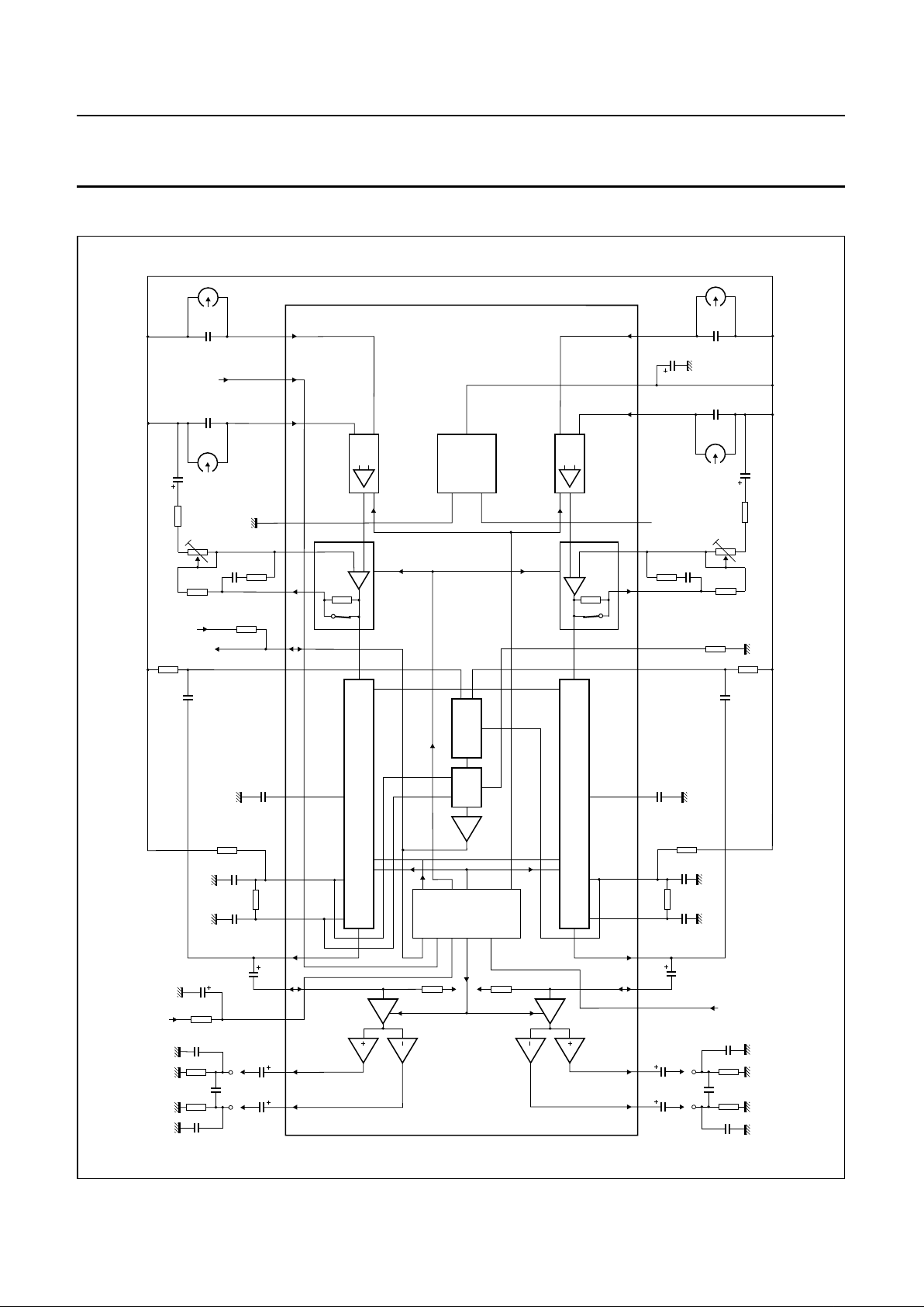
BLOCK DIAGRAM
handbook, full pagewidth
19
180 Ω
V
CC
10 µF
24
kΩ
18
kΩ
27
kΩ
8.2
kΩ
330
kΩ
1 kΩ
470
pF
470
pF
10
nF
4.7 nF
270 kΩ
180 kΩ
24
kΩ
4.7 µF
4.7 µF
1 µF
4.7 nF
15 nF
100
µF
330
nF
100
nF
C
L
R
L
R
L
R
t
AMS
delay
time
output
A+
output
A−
V
ref
MED769
from
microprocessor
LOW: NR ON
OPEN: OFF
HIGH: AMS ON
180 Ω
10 µF
8.2
kΩ
330
kΩ
1 kΩ
470
pF
470
pF
10
nF
270 kΩ
180 kΩ
4.7 µF
10
µF
4.7 µF
1 µF
15 nF
330
nF
100
nF
C
L
R
L
R
L
output
B+
output
B−
V
ref
from
microprocessor
LOW: MUTE ON
HIGH: MUTE OFF
LOW: INPUT 1
HIGH: INPUT 2
from
microprocessor
EQ switch from
microprocessor
LOW: 120 µs
OPEN: 70 µs
AMS
out
head switch
input
15
kΩ
15
kΩ
DELAY
TIME
LEVEL
DETECTOR
POWER
SUPPLY
AMS
EQ
NR
MUTE
HEAD-
SWITCH
LOGIC
DOLBY B NR CIRCUIT
DOLBY B NR CIRCUIT
1
23
4
5
6
7
8
910
11
12
13
14
15 16
17
18
20
21
22
23
24
25
26
27
28
29
30
31
32
AMS
PROCESSOR
GND
V
CC
V
ref
TEA0678
EQ
AMP.
EQ
AMP.
PRE
AMP.
PRE
AMP.
Fig.1 Block and application diagram.
Page 4
1996 Jun 06 4
Philips Semiconductors Preliminary specification
Dual Dolby* B-type noise reduction circuit, automatic
music search, with differential outputs and mute
TEA0678
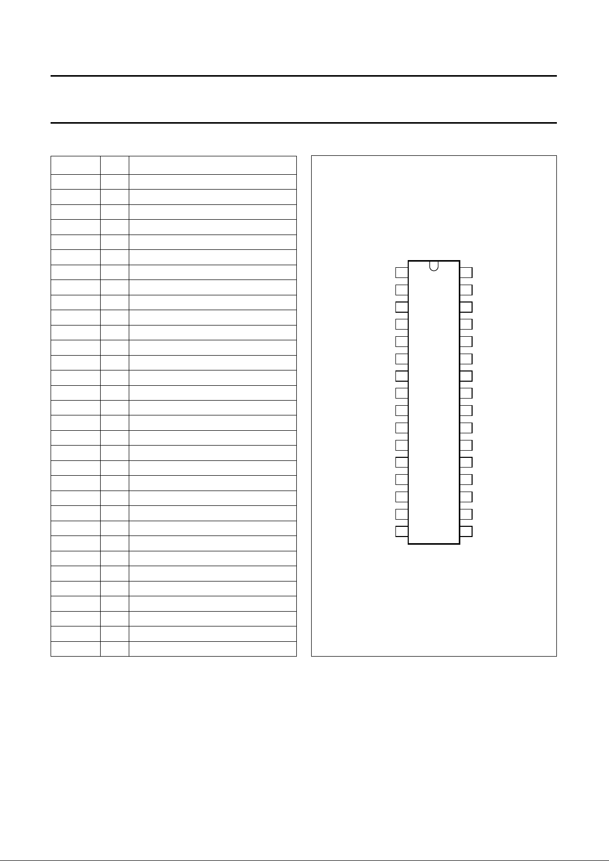
PINNING
SYMBOL PIN DESCRIPTION
OUTA− 1 negative output channel A
OUTA+ 2 positive output channel A
NR/AMS 3 noise reduction/music search switch
INCA 4 input mute/output stage channel A
OUTCA 5 output Dolby B processor channel A
INTA 6 integrating filter channel A
CONTRA 7 control voltage channel A
HPA 8 high-pass filter channel A
SCA 9 side chain channel A
TD 10 delay time constant
EQA 11 equalizing output channel A
EQFA 12 equalizing feedback channel A
V
CC
13 supply voltage
INA1 14 input channel A1 (forward or reverse)
V
ref
15 reference voltage
INA2 16 input channel A2 (reverse or forward)
INB2 17 input channel B2 (reverse or forward)
HS 18 head switch input
INB1 19 input channel B1 (forward or reverse)
GND 20 ground
EQFB 21 equalizing feedback channel B
EQB 22 equalizing output channel B
AMSEQ 23 AMS output and EQ switch input
SCB 24 side chain channel B
HPB 25 high-pass filter channel B
CONTRB 26 control voltage channel B
INTB 27 integrating filter channel B
OUTCB 28 output Dolby B processor channel B
INCB 29 input mute/output stage channel B
MUTE 30 mute switch
OUTB+ 31 positive output channel B
OUTB− 32 negative output channel B
Fig.2 Pin configuration.
handbook, halfpage
TEA0678
MED770
1
2
3
4
5
6
7
8
9
10
11
12
13
14
15
16
32
31
30
29
28
27
26
25
24
23
22
21
20
19
18
17
OUTA−
OUTA+
NR/AMS
INCA
OUTCA
INTA
CONTRA
HPA
SCA
TD
EQA
EQFA
V
CC
INA1
OUTB−
OUTB+
MUTE
INCB
INTB
CONTRB
OUTCB
HPB
SCB
AMSEQ
EQB
EQFB
GND
INB1
V
ref
INA2
HS
INB2
Page 5
1996 Jun 06 5
Philips Semiconductors Preliminary specification
Dual Dolby* B-type noise reduction circuit, automatic
music search, with differential outputs and mute
TEA0678
FUNCTIONAL DESCRIPTION
Noise Reduction (NR) is enabled when pin NR/AMS is
connected to ground and disabled when open-circuit (left
floating from a 3-state output).
Dolby noise reduction only operates correctly if 0 dB Dolby
level is adjusted at 387.5 mV.
Automatic Music Search (AMS) is enabled when pin
NR/AMS is connected to HIGH (5 V) and disabled when
open-circuit (left floating from a 3-state output). In AMS
mode the signal of both channels are rectified and then
added. This means, even if one channel signal appears
inverted to the other channel, with the TEA0678 the normal
AMS function is ensured (see Figs 4, 5 and 6).
Equalization time constant switching (70 µs or 120 µs)
is achieved when pin AMSEQ is connected to GND via an
18 kΩ resistor (120 µs), or left open-circuit (70 µs).
This does not affect the AMS output signal during AMS
mode (see Fig.1).
Head switching is achieved when pin HS is connected to
GND (input IN1 active) or connected to HIGH (5 V) level
(input IN2 active). If left open-circuit IN1 is active.
Mute is enabled when pin MUTE is connected to ground
and off when connected to HIGH (5 V) level. For smooth
switching a time constant is recommended. If left
open-circuit MUTE is active.
The differential output stage of each channel is
connected via a provision to the Dolby and pre-amplifier
part. This provision may be used for any processing of the
tape signal or to add another signal. Each output drives a
resistive load of nominal 10 kΩ and is capable of driving
1kΩ, also a capacitive load of 1.2 nF to ground and
between differential outputs. Each output can be
short-circuited to a battery (16 V) via a coupling capacitor
(4.7 µF).
LIMITING VALUES
In accordance with the Absolute Maximum Rating System (IEC 134); note1.
Notes
1. The device may not operate correctly when subjected to these ratings when the ratings exceed the electrical
characteristics of the device as specified in Chapter “Characteristics”. The device will recover automatically when the
environment is reduced to the requirements of the characteristics.
2. The TEA0678 allows a HIGH-level at switching pins without supply voltage (V
CC
= 0; stand-by mode). This means a
maximum input voltage of 6.5 V for the switching input pins.
3. Human body model (1.5 kΩ, 100 pF).
4. Machine model (0 Ω, 200 pF).
SYMBOL PARAMETER CONDITIONS MIN. MAX. UNIT
V
CC
supply voltage 0 16 V
V
i
input voltage (pins 1 to 32) except pin 15 (V
ref
); pin 3
(NR/AMS), pin 18 (HS) and pin 30 (MUTE) to V
CC
−0.3 +V
CC
V
input voltage at pin 3 (NR/AMS), pin 18 (HS) and
pin 30 (MUTE)
note 2 −0.3 +6.5 V
t
short
pin 15 (V
ref
) to VCC short-circuiting duration − 5s
T
stg
storage temperature −55 +150 °C
T
amb
operating ambient temperature −40 +85 °C
V
es
electrostatic handling voltage for all pins note 3 −2+2kV
note 4 −500 +500 V
Page 6
1996 Jun 06 6
Philips Semiconductors Preliminary specification
Dual Dolby* B-type noise reduction circuit, automatic
music search, with differential outputs and mute
TEA0678
CHARACTERISTICS
VCC= 10 V; f = 20 Hz to 20 kHz; T
amb
=25°C; nominal load 10 kΩ; all levels are referenced to 775 mV (RMS) (0 dB) at
differential outputs (Vo=Vo+− Vo−), this corresponds to Dolby level 387.5 mV (RMS) (0 dB) at test point (OUTC);
see Fig.1; NR on/AMS off; EQ switch in the 70 µs position; unless otherwise specified.
SYMBOL PARAMETER CONDITIONS MIN. TYP. MAX. UNIT
V
CC
supply voltage 7.6 10 12 V
I
CC
supply current pins 14, 16, 17 and 19 connected to
V
ref
− 25 28 mA
f = 1 kHz; V
o
= 0 dB at each output − 26 37 mA
α
m
channel matching f = 1 kHz; Vo= 0 dB; NR off;
OUTA/OUTB
−0.5 − +0.5 dB
G
v
voltage gain (output stage) between OUT and OUTC; f = 1 kHz;
NR off
5.5 6 6.5 dB
G
mm
voltage gain mismatch
(output stage)
mismatch between OUT+ and
OUT−; f = 1 kHz; NR off
−0.5 − +0.5 dB
THD total harmonic distortion (2nd
and 3rd harmonic)
f = 1 kHz; V
o
=0dB − 0.08 0.15 %
f = 10 kHz; V
o
=6dB − 0.15 0.3 %
H
R
headroom at output VCC= 9 V; THD = 1%; f = 1 kHz 13 −−dB
signal plus noise-to-noise
ratio
internal gain 40 dB; linear;
CCIR/ARM weighted; decode mode;
see Fig.10
78 84 − dB
V
no(rms)
equivalent input noise voltage
in decode mode (RMS value)
NR off; unweighted;
f = 20 Hz to 20 kHz; R
source
=0Ω
−− 1.4 µV
PSRR power supply ripple rejection V
i(rms)
= 0.25 V; f = 1 kHz; see Fig.7
for unsymmetrical signal at OUTC
52 57 − dB
at differential OUT; note 1 49 52 − dB
f
o
frequency response
measured in encode mode;
referenced to TP
see Fig.10
V
o
= −25 dB; f = 0.2 kHz −22.9 −24.4 −25.9 dB
V
o
= 0 dB; f=1kHz −1.5 0 +1.5 dB
V
o
= −25 dB; f=1kHz −17.8 −19.3 −20.8 dB
V
o
= −25 dB; f=5kHz −18.1 −19.6 −21.1 dB
V
o
= −35 dB; f = 10 kHz −24.4 −25.9 −27.4 dB
α
cs
channel separation Vo= +10 dB; f = 1 kHz; see Fig.8 61 67 − dB
α
cc
crosstalk between active and
inactive input
NR off; f = 1 kHz; Vo= +10 dB;
see Fig.8
70 77 − dB
R
L
load resistance at each output
OUTA+, OUTA−, OUTB+ and
OUTB− (corresponds to 2 kΩ
at differential output)
AC-coupled f = 1 kHz; Vo= 12 dB;
THD=1%
10 −−kΩ
THD = 1%; note 2 1 −−kΩ
C
L
capacitive load at each output
(between OUT+ and OUT−)
and ground
C
Lmin
at each output to ground
(pins 1, 2, 31 and 32)
0.3 − 1.3 nF
G
v
voltage gain of pre-amplifier from pin INA1 or INA2 to pin EQFA
and from pin INB1 or INB2 to
pin EQFB; f = 1 kHz
29 30 31 dB
SN+
N
--------------
Page 7

1996 Jun 06 7
Philips Semiconductors Preliminary specification
Dual Dolby* B-type noise reduction circuit, automatic
music search, with differential outputs and mute
TEA0678
V
I(offset)(DC)
DC input offset voltage − 2 − mV
I
i(bias)
input bias current −− 0.4 µA
R
EQ
equalization resistor 4.7 5.8 6.9 kΩ
R
I
input resistance head inputs 60 100 − kΩ
A
v
open-loop amplification pin INA1 or INA2 to pin EQA and
pin INB1 or INB2 to pin EQB
f = 10 kHz 80 86 − dB
f = 400 Hz 104 110 − dB
V
O(offset)(DC)
DC offset voltage at pins
OUT+ to OUT−
pins INA1, INA2, INB1 and INB2
connected to V
ref
−10 − +10 mV
V
mute(offset)
MUTE offset voltage at pins
OUT+ to OUT−
pins INA1, INA2, INB1 and INB2
connected to V
ref
−10 − +10 mV
V
ref
− V
OUTC
DC output offset voltage at
pins OUTCA and OUTCB
NR off; pins INA1, INA2, INB1 and
INB2 connected to V
ref
−0.15 − +0.15 V
I
O
DC output current pins INA1, INA2, INB1 and INB2
connected to V
ref
pin OUTC to ground −2 −−mA
pin OUTC to V
CC
0.3 −−mA
pin OUT± to ground −2.5 −−mA
pin OUT± to V
CC
2.5 −−mA
R
i
input resistance output stage
at pins INCA and INCB
10 16 − kΩ
Z
o
output impedance at each
output OUTA+, OUTA−,
OUTB+ and OUTB−
− 90 110 Ω
d
mute
mute depth at differential
output
NR off
f = 1 kHz −80 −−dB
f = 10 kHz −80 −−dB
AMSL AMS threshold level at
music to pause
NR off;f=10kHz; see Fig.9 −25 −22 −19 dB
AMSH AMS threshold level at
pause to music
note 3 −24 −21 −18 dB
t
d
AMS delay time range f = 10 kHz; 0 dB burst; see Table 1 − 23 to 160 − ms
t
r
AMS rise/delay time f = 10 kHz; 0 dB burst 2 − 10 ms
EMC DC offset voltage at
pins OUTA−, OUTA+,
OUTB+ and OUTB−
f = 900 MHz; V
i
=3V
(RMS)
;
see Figs 11, 12 and13
− 100 − mV
SYMBOL PARAMETER CONDITIONS MIN. TYP. MAX. UNIT
Page 8
1996 Jun 06 8
Philips Semiconductors Preliminary specification
Dual Dolby* B-type noise reduction circuit, automatic
music search, with differential outputs and mute
TEA0678
Switching thresholds
NR/AMS SWITCH (PIN 3)
V
IL
LOW level input voltage NR on −0.3 − +0.8 V
I
IL
LOW level input current NR on −10 −20 −40 µA
I
i(float)
allowed floating input current pin left open-circuit; NR/AMS off −10 0 +10 µA
V
float
floating voltage pin left open-circuit; NR/AMS off − 2.4 5 V
V
IH
HIGH level input voltage AMS on 4 − 5.5 V
I
IH
HIGH level input current AMS on 10 20 40 µA
EQUALIZATION (PIN 23)
I
EQ70
floating leakage current time constant 70 µs active +0.002 −−0.15 mA
V
EQ70
floating voltage time constant 70 µs active − 4.6 5 V
I
EQ120
input current time constant 120 µs active −0.25 −−1mA
AMS OUTPUT (PIN 23)
V
OH
HIGH level output voltage music present 4 4.6 5 V
I
OH
HIGH level output current current capability +0.01 −−1mA
I
OH
HIGH level output current current capability; note 4 +0.01 −−0.15 mA
V
OL
LOW level output voltage music not present −− 0.8 V
I
OL
LOW level output current current capability −0.01 − +1 mA
MUTE SWITCH (PIN 30)
V
IL
LOW level input voltage MUTE on −0.3 − +0.8 V
I
IL
LOW level input current MUTE on −−4 −100 µA
V
IH
HIGH level input voltage MUTE off 4 − 5.5 V
I
IH
HIGH level input current MUTE off; smooth switching with a
time constant is recommended
− 10 100 µA
HEAD SWITCH (PIN 18)
V
IL
LOW level input voltage INPUT 1 on −0.3 − +0.8 V
I
IL
LOW level input current INPUT 1 on −− −100 µA
V
IH
HIGH level input voltage INPUT 2 on 4 − 5.5 V
I
IH
HIGH level input current INPUT 2 on − 30 100 µA
SYMBOL PARAMETER CONDITIONS MIN. TYP. MAX. UNIT
Page 9

1996 Jun 06 9
Philips Semiconductors Preliminary specification
Dual Dolby* B-type noise reduction circuit, automatic
music search, with differential outputs and mute
TEA0678
Notes to the characteristics
1. For the signal to be doubled (+6 dB) at differential output as a function of OUTC, the signal-to-ripple ratio is improved
at differential output for approximately 3 dB.
2. By using the small load, the output voltage may be divided by −0.8 dB.
3. The high speed of the tape (FF, REW) at the tape head during AMS mode causes a transformation of level and
frequency of the originally recorded signal. It means a boost of signal level of approximately 10 dB and more for
recorded frequencies from 500 Hz up to 4 kHz. So the threshold level of −22 dB corresponds to signal levels in
PB mode of approximately −32 dB. The AMS inputs for each channel are pin SCA and pin SCB. As the frequency
spectrum is transformed by a factor of approximately 10 to 30 due to the higher tape speed in FF, REW, the
high-pass filter (4.7 nF/24 kΩ) removes the effect of offset voltages but does not affect the music search function.
In the application circuit (Fig.1) the frequency response of the system between tape heads input, e.g. pins INA2/INB2,
to the AMS input pins SCA and SCB is constant over the whole frequency range (see Fig.3). The frequency
dependence of threshold level is shown in Fig.3.
4. In AMS OFF mode, pin AMSEQ is HIGH level, the equalization time constant will be switched by pulling
approximately 200 µA out of pin AMSEQ. This means for the device connected to pin AMSEQ, a restriction of input
current at HIGH level less than 200 µA during AMS off; otherwise the switching of the time constants is disabled but
fixed at 120 µs. If the following devices, input consumes more than 200 µA, this input has to be disconnected in AMS
off mode. (To ensure switching the currents for the different switched modes are specified with a tolerance of±50 µA
in Chapter “Characteristics”.) For an application with a fixed EQ time constant of 120 µs the equalizing network may
be applied completely external. Change 8.2 kΩ resistor to 14 kΩ the internal resistor REQ= 5.8 kΩ is short-circuited
by fixing the EQ switch input at the 70 µs position (I
EQ70
).
Table 1 Blank delay time set by resistor R
t
at pin TD
RESISTOR VALUE R
t
(kΩ)
DELAY TIME t
d
TYP. (ms)
TOLERANCE
(%)
68 23 20
150 42 15
180 48 15
220 56 15
270 65 10
330 76 10
470 98 10
560 112 10
680 126 10
820 142 10
1000 160 10
Page 10

1996 Jun 06 10
Philips Semiconductors Preliminary specification
Dual Dolby* B-type noise reduction circuit, automatic
music search, with differential outputs and mute
TEA0678
General note
It is recommended to switch off VCC with a gradient of 400 V/s at maximum to avoid plops on tape in the event of contact
between tape and tape head while switching off.
Fig.3 AMS threshold level.
(1) AMS threshold level for application circuit (Fig.1).
(2) AMS threshold level for test circuit (Fig.9).
handbook, full pagewidth
−60
−20
MED623
10
2
10
3
10
4
10
5
−40
−50
−30
(dB)
(Hz)
(1)
(2)
General note on AMS
The speed of tape at the tape head during FF, REW
depends on the diameter of the tape on the spindle.
Depending on this speed, the recorded signal occurs
transformed in frequency and magnitude as a function of
the original signal in playback mode speed. For example:
A recorded pause of 3 s passes the tape head at its
highest speed in 111 ms, e.g. during FF mode near tape
end. This time constant of 111 ms corresponds to a pause
of 1.3 s at the beginning of the tape in playback mode.
Thus a pause T is uniquely defined outside the interval
1.3 s < T < 3 s. Inside this interval T will be recognized as
a pause or not dependent on the local point of tape,
respectively the speed of tape. Times of pauses described
investigated for this document are valid for tape devices
with a speed of its spindle (FF, REW):
respectively 12 to 27 times of the playback speed.
ωr51
1
s
-- -
=
Page 11

1996 Jun 06 11
Philips Semiconductors Preliminary specification
Dual Dolby* B-type noise reduction circuit, automatic
music search, with differential outputs and mute
TEA0678
Short description ‘music search’
A system for ‘music search’ mainly consists of a level and
a time detection (see Fig.4). For adapting and decoupling
the input signal will be amplified (A), then rectified (B) and
smoothed with a time constant (C). So the voltage at (C)
corresponds to the signal level and will be compared to the
predefined pause level at the first comparator (D), the level
detector. If the signal level becomes smaller than the
pause level, the level detector(D) changes its output
signal. Due to the output level of the level detector the
capacitor of the second time constant (E) will be charged,
respectively discharged. If the pause level of the input
signal remains for a certain time, the voltage at the
capacitor reaches a certain value, which corresponds to
an equivalent time value due to the charging. The voltage
at the capacitor will be compared to a predefined
time-equivalent voltage by the second comparator (F), the
time detector. If the pause level of the input signal remains
for this predefined time, the time detector (F) changes its
output level for ‘pause found’ status.
In this IC the signals of both channels are first rectified and then added. The signal behind the adder is described by
V
add
= V
chanA
+ V
chanB
, where:
V
chanA
: absolute value channel A
V
chanB
: absolute value channel B
This means, even if one channel signal appears phase shifted to the other channel (at worst cases inverted), the
TEA0678 will ensure the normal AMS function.
Fig.4 Integrated ‘music search’ function.
handbook, full pagewidth
MED772
COMPARATOR 1 COMPARATOR 2
t
1
t
2
INA
INB
AMPLIFIER
RECTIFIER
(A)
(B)
(C)
(D)
(E) (F)
OUT
V
t
V
I
LEVEL DETECTOR TIME DETECTOR
Page 12

1996 Jun 06 12
Philips Semiconductors Preliminary specification
Dual Dolby* B-type noise reduction circuit, automatic
music search, with differential outputs and mute
TEA0678
Description of the principle timing diagram for AMS-scan mode without initial input signal (see Fig.5)
Fig.5 AMS-scan mode without initial input signal.
handbook, full pagewidth
MED773
output signal
to microprocessor
4.5 V
V
AMSEQ
time threshold
upper threshold
(hysteresis)
V
t
V
REF
level threshold
V
l
V
in
tr: rise time
td: delay time
tb: burst time
tp: pause time
tf: fall time
Vl: voltage at
level detector
input
pin 7 (CONTRA)
Vt: voltage at
time detector
input
pin 26 (CONTRB)
t
t
t
t
AMS on
t
r
t
d
t
f
tb<t
r
tp<t
d
t
0
t3t
4t5t6
t
7
t8t9t
10
t11t12t13t
14t15
By activating AMS-scan mode, the AMS output level
directly indicates whether the input level corresponds to a
pause level (V
AMSEQ
= LOW) or not (V
AMSEQ
= HIGH).
At t0 the AMS-scan mode is activated. Without a signal at
Vin, the following initial procedure runs until the AMS
output changes to LOW level: due to no signal at Vin the
voltage at the level detector input VI (pin 7, CONTRA)
remains below the level threshold and the second time
constant will be discharged (time detector input Vt).
When Vt passes the time threshold level, the time detector
output changes to LOW level. Now the initial procedure is
completed.
If a signal burst appears at t3, the level detector input
voltage rises immediately and causes its output to charge
the second time constant, which supplies the input voltage
Vt for the time detector. When Vt passes the upper
threshold level after the rise time tr (at t4), the AMS output
changes to HIGH. If the signal burst ends at t5 the level
detector input VI falls to its LOW level. When passing the
level threshold at t6, the discharging of the second time
constant begins. Now the circuit measures the delay time
td, which is externally fixed by a resistor and defines the
length of a pause to be detected. If no signal appears at V
in
within the time interval td, the time detector output switches
the AMS output to LOW level at t7.
If a plop noise pulse appears at Vin (t8) with a pulse width
less than the rise time tr>tb, the plop noise will not be
detected as music. The AMS output remains LOW.
Similarly the system handles ‘no music pulses’ tp: when
music appears at t11 with a small interruption at t13, this
interruption will not affect the AMS output for tp<td.
Page 13

1996 Jun 06 13
Philips Semiconductors Preliminary specification
Dual Dolby* B-type noise reduction circuit, automatic
music search, with differential outputs and mute
TEA0678
Description of the principle timing diagram for AMS-scan mode with initial input signal (see Fig.6)
Fig.6 AMS-scan mode with initial input signal.
handbook, full pagewidth
MED774
output signal
to microprocessor
4.5 V
V
AMSEQ
time threshold
upper threshold
(hysteresis)
V
t
V
REF
level threshold
V
l
V
in
tr: rise time
td: delay time
tb: burst time
tp: pause time
tf: fall time
Vl: voltage at
level detector
input
pin 7 (CONTRA)
Vt: voltage at
time detector
input
pin 26 (CONTRB)
t
t
t
t
AMS on
t
d
t
f
tb<t
r
tp<t
r
t0t
1
t5t
6
t
7
t8t9t
10
t11t12t13t
14
t
15
At t0 the AMS-scan mode is activated. With an input signal
at Vin, the following initial procedure runs until the circuit
gets a steady state status.
Due to the signal at Vin the voltage at the level detector
input VI (pin 7, CONTRA) slides to a value which is defined
by a limiter. This voltage causes the level detector output
charging the second time constant (time detector input Vt)
to its maximum voltage level at t1. Now the initial
procedure is completed.
The following behaviour does not differ from the
description in Section “Description of the principle timing
diagram for AMS-scan mode without initial input signal
(see Fig.5)”.
Page 14

1996 Jun 06 14
Philips Semiconductors Preliminary specification
Dual Dolby* B-type noise reduction circuit, automatic
music search, with differential outputs and mute
TEA0678
TEST AND APPLICATION INFORMATION
andbook, full pagewidth
10 kΩ
1000
µF
100
nF
270 kΩ
180 kΩ
10 kΩ
20 kΩ
24
kΩ
18 kΩ
20 kΩ
10 kΩ
24 kΩ
270 kΩ
180 kΩ
27
kΩ
4.7 µF
4.7 µF
1 µF
10 µF
10 µF
10 µF
1 µF
4.7 µF
4.7 µF
4.7 nF
15 nF
15 nF
4.7 nF
100
µF
100
nF
330
nF
100
nF
330
nF
C
L
R
L
R
L
C
L
R
L
R
L
output
B−
output
B+
from
microprocessor
HIGH: MUTE OFF
V
ref
AMS
out
EQ
70 µs
from
microprocessor
LOW: INPUT 1
HIGH: INPUT 2
R
t
AMS
delay
time
output
A+
output
A−
ON
NR
LOW: NR ON
V
ref
V
CC
= 10 V
0.25 V RMS
1 kHz
15
kΩ
15
kΩ
DELAY
TIME
LEVEL
DETECTOR
POWER
SUPPLY
AMS
EQ
NR
MUTE
HEAD-
SWITCH
LOGIC
DOLBY B NR CIRCUIT
DOLBY B NR CIRCUIT
1
23
4
5
6
7
8
910
11
12
13
14
15 16
17
18
1920
21
22
23
24
25
26
27
28
29
30
31
32
AMS
PROCESSOR
GND
V
CC
V
ref
TEA0678
EQ
AMP.
EQ
AMP.
PRE
AMP.
PRE
AMP.
MED775
Fig.7 Test circuit for power supply ripple rejection.
Page 15

1996 Jun 06 15
Philips Semiconductors Preliminary specification
Dual Dolby* B-type noise reduction circuit, automatic
music search, with differential outputs and mute
TEA0678
ndbook, full pagewidth
19
200
Ω
470
pF
10
µF
100
nF
270 kΩ
180 kΩ
10 kΩ
20 kΩ
24
kΩ
4.7 µF
4.7 µF
1 µF
10 µF
4.7 nF
15 nF
100
µF
330
nF
100
nF
C
L
R
L
R
L
R
t
AMS
delay
time
output
A+
output
A−
ON
NR
LOW: NR ON
V
ref
V
CC
= 10 V
MED776
10 V
18 kΩ
20 kΩ
10 kΩ
24 kΩ
270 kΩ
180 kΩ
27
kΩ
10 µF
10 µF
1 µF
4.7 µF
4.7 µF
15 nF
4.7 nF
100
nF
330
nF
C
L
R
L
R
L
output
B−
output
B+
from
microprocessor
HIGH: MUTE OFF
V
ref
AMS
out
EQ
70 µs
from
microprocessor
LOW: INPUT 1
HIGH: INPUT 2
15
kΩ
15
kΩ
DELAY
TIME
LEVEL
DETECTOR
POWER
SUPPLY
AMS
EQ
NR
HEAD-
SWITCH
MUTE
LOGIC
DOLBY B NR CIRCUIT
DOLBY B NR CIRCUIT
1
23
4
5
6
7
8
910
11
12
13
14
15 16
17
18
20
21
22
23
24
25
26
27
28
29
30
31
32
AMS
PROCESSOR
GND
V
CC
V
ref
TEA0678
EQ
AMP.
EQ
AMP.
PRE
AMP.
PRE
AMP.
Fig.8 Test circuit for channel separation.
Page 16

1996 Jun 06 16
Philips Semiconductors Preliminary specification
Dual Dolby* B-type noise reduction circuit, automatic
music search, with differential outputs and mute
TEA0678
handbook, full pagewidth
19
100
nF
270 kΩ
180 kΩ
10 kΩ
20 kΩ
24
kΩ
4.7 µF
4.7 µF
1 µF
10 µF
4.7 nF
15 nF
100
µF
330
nF
100
nF
C
L
R
L
R
L
R
t
AMS
delay
time
output
A+
output
A−
V
ref
V
CC
= 10 V
5 V
HIGH: AMS ON
18 kΩ
20 kΩ
10 kΩ
24 kΩ
270 kΩ
180 kΩ
27
kΩ
10 µF
10 µF
1 µF
4.7 µF
4.7 µF
15 nF
4.7 nF
100
nF
330
nF
C
L
R
L
R
L
output
B−
output
B+
from
microprocessor
HIGH: MUTE OFF
V
ref
AMS
out
EQ
70 µs
from
microprocessor
LOW: INPUT 1
HIGH: INPUT 2
15
kΩ
15
kΩ
DELAY
TIME
LEVEL
DETECTOR
POWER
SUPPLY
AMS
EQ
NR
HEAD-
SWITCH
MUTE
LOGIC
DOLBY B NR CIRCUIT
DOLBY B NR CIRCUIT
1
23
4
5
6
7
8
910
11
12
13
14
MED777
15 16
17
voltage
input
18
20
21
22
23
24
25
26
27
28
29
30
31
32
AMS
PROCESSOR
GND
V
CC
V
ref
TEA0678
EQ
AMP.
EQ
AMP.
PRE
AMP.
PRE
AMP.
Fig.9 Test circuit for AMS threshold level.
Page 17

1996 Jun 06 17
Philips Semiconductors Preliminary specification
Dual Dolby* B-type noise reduction circuit, automatic
music search, with differential outputs and mute
TEA0678
handbook, full pagewidth
MED778
15
kΩ
15
kΩ
270 kΩ
180 kΩ
10 kΩ
20 kΩ
24
kΩ
18 kΩ
20 kΩ
10 kΩ
25 kΩ
25 kΩ
24 kΩ
270 kΩ
180 kΩ
27
kΩ
4.7 µF
4.7 µF
1 µF
10 µF
10 µF
10 µF
10 µF
1 µF
4.7 µF
4.7 µF
4.7 nF
15 nF
15 nF
200
Ω
100
µF
10
µF
100
nF
330
nF
100
nF
100
nF
470
pF
4.7
nF
330
nF
DELAY
TIME
LEVEL
DETECTOR
POWER
SUPPLY
AMS
EQ
NR
HEAD-
SWITCH
MUTE
HEAD
LOGIC
DOLBY B NR CIRCUIT
DOLBY B NR CIRCUIT
1
23
4
5
6
7
8
910
11
12
13
14
15 16
17
18
1920
21
22
23
24
25
26
27
28
29
30
31
32
C
L
R
L
R
L
C
L
R
L
R
L
output
B−
output
B+
from
microprocessor
HIGH: MUTE OFF
V
ref
TP
AMS
out
EQ
70 µs
V
CC
V
i
from
microprocessor
LOW: INPUT 1
HIGH: INPUT 2
R
t
AMS
delay
time
output
A+
output
A−
ON
NR
LOW: NR ON
V
ref
V
CC
= 10 V
10 V
V
i
AMS
PROCESSOR
GND
V
CC
V
ref
TEA0678
EQ
AMP.
EQ
AMP.
PRE
AMP.
PRE
AMP.
TP
Fig.10 Test circuit for frequency response (channel B, encode mode).
Page 18

1996 Jun 06 18
Philips Semiconductors Preliminary specification
Dual Dolby* B-type noise reduction circuit, automatic
music search, with differential outputs and mute
TEA0678
ndbook, full pagewidth
19
100
nF
270 kΩ
180 kΩ
10 kΩ
20 kΩ
68 kΩ
24
kΩ
4.7
µF
4.7
µF
4.7 nF
15 nF
100
µF
330
nF
100
nF
10 Ω
40 Ω
AMS
delay
time
V
CC
= 10 V
MBH478
20 kΩ
10 kΩ
24 kΩ
270 kΩ
180 kΩ
27
kΩ
5 kΩ
V
CC
5 kΩ
10 µF
15 nF
4.7 nF
100
nF
330
nF
V
ref
200
Ω
470
pF
200
Ω
470
pF
200
Ω
470
pF
15
kΩ
15
kΩ
DELAY
TIME
LEVEL
DETECTOR
4.7
µF
4.7
µF
POWER
SUPPLY
200
Ω
470
pF
AMS
EQ
NR
HEAD-
SWITCH
MUTE
LOGIC
DOLBY B NR CIRCUIT
DOLBY B NR CIRCUIT
1
23
4
5
6
7
8
910
11
12
13
14
15 16
17
18
20
21
22
23
24
25
26
27
28
29
30
31
32
AMS
PROCESSOR
GND
V
CC
V
ref
TEA0678
EQ
AMP.
EQ
AMP.
PRE
AMP.
PRE
AMP.
Fig.11 EMC test circuit.
Page 19

1996 Jun 06 19
Philips Semiconductors Preliminary specification
Dual Dolby* B-type noise reduction circuit, automatic
music search, with differential outputs and mute
TEA0678
LAYOUT OF PRINTED-CIRCUIT BOARD FOR EMC TEST CIRCUIT (FOR TEA0678T)
Fig.12 Top side with components.
Dimensions in mm.
pagewidth
MBH462
68
72
40 Ω
470 pF
10 Ω
200 Ω
0 Ω
0 Ω
0 Ω
0 Ω
470 pF
200 Ω
270
kΩ
270
kΩ
27 kΩ
5 kΩ5 kΩ
20
kΩ
20
kΩ
10 kΩ
470 pF
200 Ω
470 pF
200 Ω
10 kΩ
68 kΩ
15 nF15 nF
4.7 nF4.7 nF
100 nF100 nF
100 nF
TEA0678T
Page 20

1996 Jun 06 20
Philips Semiconductors Preliminary specification
Dual Dolby* B-type noise reduction circuit, automatic
music search, with differential outputs and mute
TEA0678
Fig.13 Bottom side with components.
pagewidth
MBH461
72
68
X5
X4
X3
MP
MP
MP
MP
MP
MP
MP
4.7 µF
100 µF
100 µF
4.7 µF 4.7 µF
180 kΩ
180 kΩ
24 kΩ
24 kΩ
4.7 µF
X2
X1 S1
X5
330 nF
330 nF
Dimensions in mm.
Page 21

1996 Jun 06 21
Philips Semiconductors Preliminary specification
Dual Dolby* B-type noise reduction circuit, automatic
music search, with differential outputs and mute
TEA0678
PACKAGE OUTLINES
UNIT b
1
cEe M
H
L
REFERENCES
OUTLINE
VERSION
EUROPEAN
PROJECTION
ISSUE DATE
IEC JEDEC EIAJ
mm
DIMENSIONS (mm are the original dimensions)
SOT232-1
92-11-17
95-02-04
b
max.
w
M
E
e
1
1.3
0.8
0.53
0.40
0.32
0.23
29.4
28.5
9.1
8.7
3.2
2.8
0.181.778 10.16
10.7
10.2
12.2
10.5
1.6
4.7 0.51 3.8
M
H
c
(e )
1
M
E
A
L
seating plane
A
1
w M
b
1
e
D
A
2
Z
32
1
17
16
b
E
pin 1 index
0 5 10 mm
scale
Note
1. Plastic or metal protrusions of 0.25 mm maximum per side are not included.
(1) (1)
D
(1)
Z
A
max.
12
A
min.
A
max.
SDIP32: plastic shrink dual in-line package; 32 leads (400 mil)
SOT232-1
Page 22

1996 Jun 06 22
Philips Semiconductors Preliminary specification
Dual Dolby* B-type noise reduction circuit, automatic
music search, with differential outputs and mute
TEA0678
UNIT
A
max.
A
1
A
2
A3b
p
cD
(1)E(1)
eHELLpQZywv θ
REFERENCES
OUTLINE
VERSION
EUROPEAN
PROJECTION
ISSUE DATE
IEC JEDEC EIAJ
mm
inches
2.65
0.10
0.25
0.01
1.4
0.055
0.3
0.1
2.45
2.25
0.49
0.36
0.27
0.18
20.7
20.3
7.6
7.4
1.27
10.65
10.00
1.2
1.0
0.95
0.55
8
0
o
o
0.25 0.1
0.004
0.25
DIMENSIONS (inch dimensions are derived from the original mm dimensions)
Note
1. Plastic or metal protrusions of 0.15 mm maximum per side are not included.
1.1
0.4
SOT287-1
92-11-17
95-01-25
(1)
0.012
0.004
0.096
0.086
0.02
0.01
0.050
0.047
0.039
0.42
0.39
0.30
0.29
0.81
0.80
0.011
0.007
0.037
0.022
0.010.01
0.043
0.016
w M
b
p
D
H
E
Z
e
c
v M
A
X
A
y
32
17
16
1
θ
A
A
1
A
2
L
p
Q
detail X
L
(A )
3
E
pin 1 index
0 5 10 mm
scale
SO32: plastic small outline package; 32 leads; body width 7.5 mm
SOT287-1
Page 23

1996 Jun 06 23
Philips Semiconductors Preliminary specification
Dual Dolby* B-type noise reduction circuit, automatic
music search, with differential outputs and mute
TEA0678
SOLDERING
Introduction
There is no soldering method that is ideal for all IC
packages. Wave soldering is often preferred when
through-hole and surface mounted components are mixed
on one printed-circuit board. However, wave soldering is
not always suitable for surface mounted ICs, or for
printed-circuits with high population densities. In these
situations reflow soldering is often used.
This text gives a very brief insight to a complex technology.
A more in-depth account of soldering ICs can be found in
our
“IC Package Databook”
(order code 9398 652 90011).
SDIP
S
OLDERING BY DIPPING OR BY WA VE
The maximum permissible temperature of the solder is
260 °C; solder at this temperature must not be in contact
with the joint for more than 5 seconds. The total contact
time of successive solder waves must not exceed
5 seconds.
The device may be mounted up to the seating plane, but
the temperature of the plastic body must not exceed the
specified maximum storage temperature (T
stg max
). If the
printed-circuit board has been pre-heated, forced cooling
may be necessary immediately after soldering to keep the
temperature within the permissible limit.
R
EPAIRING SOLDERED JOINTS
Apply a low voltage soldering iron (less than 24 V) to the
lead(s) of the package, below the seating plane or not
more than 2 mm above it. If the temperature of the
soldering iron bit is less than 300 °C it may remain in
contact for up to 10 seconds. If the bit temperature is
between 300 and 400 °C, contact may be up to 5 seconds.
SO
REFLOW SOLDERING
Reflow soldering techniques are suitable for all SO
packages.
Reflow soldering requires solder paste (a suspension of
fine solder particles, flux and binding agent) to be applied
to the printed-circuit board by screen printing, stencilling or
pressure-syringe dispensing before package placement.
Several techniques exist for reflowing; for example,
thermal conduction by heated belt. Dwell times vary
between 50 and 300 seconds depending on heating
method. Typical reflow temperatures range from
215 to 250 °C.
Preheating is necessary to dry the paste and evaporate
the binding agent. Preheating duration: 45 minutes at
45 °C.
W
AVE SOLDERING
Wave soldering techniques can be used for all SO
packages if the following conditions are observed:
• A double-wave (a turbulent wave with high upward
pressure followed by a smooth laminar wave) soldering
technique should be used.
• The longitudinal axis of the package footprint must be
parallel to the solder flow.
• The package footprint must incorporate solder thieves at
the downstream end.
During placement and before soldering, the package must
be fixed with a droplet of adhesive. The adhesive can be
applied by screen printing, pin transfer or syringe
dispensing. The package can be soldered after the
adhesive is cured.
Maximum permissible solder temperature is 260 °C, and
maximum duration of package immersion in solder is
10 seconds, if cooled to less than 150 °C within
6 seconds. Typical dwell time is 4 seconds at 250 °C.
A mildly-activated flux will eliminate the need for removal
of corrosive residues in most applications.
R
EPAIRING SOLDERED JOINTS
Fix the component by first soldering two diagonallyopposite end leads. Use only a low voltage soldering iron
(less than 24 V) applied to the flat part of the lead. Contact
time must be limited to 10 seconds at up to 300 °C. When
using a dedicated tool, all other leads can be soldered in
one operation within 2 to 5 seconds between
270 and 320 °C.
Page 24

1996 Jun 06 24
Philips Semiconductors Preliminary specification
Dual Dolby* B-type noise reduction circuit, automatic
music search, with differential outputs and mute
TEA0678
DEFINITIONS
LIFE SUPPORT APPLICATIONS
These products are not designed for use in life support appliances, devices, or systems where malfunction of these
products can reasonably be expected to result in personal injury. Philips customers using or selling these products for
use in such applications do so at their own risk and agree to fully indemnify Philips for any damages resulting from such
improper use or sale.
Data sheet status
Objective specification This data sheet contains target or goal specifications for product development.
Preliminary specification This data sheet contains preliminary data; supplementary data may be published later.
Product specification This data sheet contains final product specifications.
Limiting values
Limiting values given are in accordance with the Absolute Maximum Rating System (IEC 134). Stress above one or
more of the limiting values may cause permanent damage to the device. These are stress ratings only and operation
of the device at these or at any other conditions above those given in the Characteristics sections of the specification
is not implied. Exposure to limiting values for extended periods may affect device reliability.
Application information
Where application information is given, it is advisory and does not form part of the specification.
Page 25

1996 Jun 06 25
Philips Semiconductors Preliminary specification
Dual Dolby* B-type noise reduction circuit,
automatic music search, with differential
TEA0678
NOTES
Page 26

1996 Jun 06 26
Philips Semiconductors Preliminary specification
Dual Dolby* B-type noise reduction circuit,
automatic music search, with differential
TEA0678
NOTES
Page 27

1996 Jun 06 27
Philips Semiconductors Preliminary specification
Dual Dolby* B-type noise reduction circuit,
automatic music search, with differential
TEA0678
NOTES
Page 28

Internet: http://www.semiconductors.philips.com/ps/
(1) ADDRESS CONTENT SOURCE July 29, 1996
Philips Semiconductors – a worldwide company
© Philips Electronics N.V. 1996 SCA49
All rights are reserved. Reproduction in whole or in part is prohibited without the prior written consent of the copyright owner.
The information presented in this document does not form part of any quotation or contract, is believed to be accurate and reliable and may be changed
without notice. No liability will be accepted by the publisher for any consequence of its use. Publication thereof does not convey nor imply any license
under patent- or other industrial or intellectual property rights.
Netherlands: Postbus 90050, 5600 PB EINDHOVEN, Bldg. VB,
Tel. +31 40 27 83749, Fax. +31 40 27 88399
New Zealand: 2 Wagener Place, C.P.O. Box 1041, AUCKLAND,
Tel. +64 9 849 4160, Fax. +64 9 849 7811
Norway: Box 1, Manglerud 0612, OSLO,
Tel. +47 22 74 8000, Fax. +47 22 74 8341
Philippines: Philips Semiconductors Philippines Inc.,
106 Valero St. Salcedo Village, P.O. Box 2108 MCC, MAKATI,
Metro MANILA, Tel. +63 2 816 6380, Fax. +63 2 817 3474
Poland: Ul. Lukiska 10, PL 04-123 WARSZAWA,
Tel. +48 22 612 2831, Fax. +48 22 612 2327
Portugal: see Spain
Romania: see Italy
Russia: Philips Russia, Ul. Usatcheva 35A, 119048 MOSCOW,
Tel. +7 095 926 5361, Fax. +7 095 564 8323
Singapore: Lorong 1, Toa Payoh, SINGAPORE 1231,
Tel. +65 350 2538, Fax. +65 251 6500
Slovakia: see Austria
Slovenia: see Italy
South Africa: S.A. PHILIPS Pty Ltd., 195-215 Main Road Martindale,
2092 JOHANNESBURG, P.O. Box 7430 Johannesburg 2000,
Tel. +27 11 470 5911, Fax. +27 11 470 5494
South America: Rua do Rocio 220 - 5th floor, Suite 51,
CEP: 04552-903-SÃO PAULO-SP, Brazil, P.O. Box 7383 (01064-970),
Tel. +55 11 821 2333, Fax. +55 11 829 1849
Spain: Balmes 22, 08007 BARCELONA,
Tel. +34 3 301 6312, Fax. +34 3 301 4107
Sweden: Kottbygatan 7, Akalla, S-16485 STOCKHOLM,
Tel. +46 8 632 2000, Fax. +46 8 632 2745
Switzerland: Allmendstrasse 140, CH-8027 ZÜRICH,
Tel. +41 1 488 2686, Fax. +41 1 481 7730
Taiwan: PHILIPS TAIWAN Ltd., 23-30F, 66,
Chung Hsiao West Road, Sec. 1, P.O. Box 22978,
TAIPEI 100, Tel. +886 2 382 4443, Fax. +886 2 382 4444
Thailand: PHILIPS ELECTRONICS (THAILAND) Ltd.,
209/2 Sanpavuth-Bangna Road Prakanong, BANGKOK 10260,
Tel. +66 2 745 4090, Fax. +66 2 398 0793
Turkey: Talatpasa Cad. No. 5, 80640 GÜLTEPE/ISTANBUL,
Tel. +90 212 279 2770, Fax. +90 212 282 6707
Ukraine: PHILIPS UKRAINE, 2A Akademika Koroleva str., Office 165,
252148 KIEV, Tel. +380 44 476 0297/1642, Fax. +380 44 476 6991
United Kingdom: Philips Semiconductors Ltd., 276 Bath Road, Hayes,
MIDDLESEX UB3 5BX, Tel. +44 181 730 5000, Fax. +44 181 754 8421
United States: 811 East Arques Avenue, SUNNYVALE, CA 94088-3409,
Tel. +1 800 234 7381, Fax. +1 708 296 8556
Uruguay: see South America
Vietnam: see Singapore
Yugoslavia: PHILIPS, Trg N. Pasica 5/v, 11000 BEOGRAD,
Tel. +381 11 825 344, Fax.+381 11 635 777
For all other countries apply to: Philips Semiconductors, Marketing & Sales Communications,
Building BE-p, P.O. Box 218, 5600 MD EINDHOVEN, The Netherlands, Fax. +31 40 27 24825
Argentina: see South America
Australia: 34 Waterloo Road, NORTH RYDE, NSW 2113,
Tel. +61 2 805 4455, Fax. +61 2 805 4466
Austria: Computerstr. 6, A-1101 WIEN, P.O. Box 213,
Tel. +43 1 60 101, Fax. +43 1 60 101 1210
Belarus: Hotel Minsk Business Center, Bld. 3, r. 1211, Volodarski Str. 6,
220050 MINSK, Tel. +375 172 200 733, Fax. +375 172 200 773
Belgium: see The Netherlands
Brazil: see South America
Bulgaria: Philips Bulgaria Ltd., Energoproject, 15thfloor,
51 James Bourchier Blvd., 1407 SOFIA,
Tel. +359 2 689 211, Fax. +359 2 689 102
Canada: PHILIPS SEMICONDUCTORS/COMPONENTS,
Tel. +1 800 234 7381, Fax. +1 708 296 8556
China/Hong Kong: 501 Hong Kong Industrial Technology Centre,
72 Tat Chee Avenue, Kowloon Tong, HONG KONG,
Tel. +852 2319 7888, Fax. +852 2319 7700
Colombia: see South America
Czech Republic: see Austria
Denmark: Prags Boulevard 80, PB 1919, DK-2300 COPENHAGEN S,
Tel. +45 32 88 2636, Fax. +45 31 57 1949
Finland: Sinikalliontie 3, FIN-02630 ESPOO,
Tel. +358 615 800, Fax. +358 615 80920
France: 4 Rue du Port-aux-Vins, BP317, 92156 SURESNES Cedex,
Tel. +33 1 40 99 6161, Fax. +33 1 40 99 6427
Germany: Hammerbrookstraße 69, D-20097 HAMBURG,
Tel. +49 40 23 52 60, Fax. +49 40 23 536 300
Greece: No. 15, 25th March Street, GR 17778 TAVROS,
Tel. +30 1 4894 339/911, Fax. +30 1 4814 240
Hungary: see Austria
India: Philips INDIA Ltd, Shivsagar Estate, A Block, Dr. Annie Besant Rd.
Worli, MUMBAI 400 018, Tel. +91 22 4938 541, Fax. +91 22 4938 722
Indonesia: see Singapore
Ireland: Newstead, Clonskeagh, DUBLIN 14,
Tel. +353 1 7640 000, Fax. +353 1 7640 200
Israel: RAPAC Electronics, 7 Kehilat Saloniki St, TEL AVIV 61180,
Tel. +972 3 645 0444, Fax. +972 3 648 1007
Italy: PHILIPS SEMICONDUCTORS, Piazza IV Novembre 3,
20124 MILANO, Tel. +39 2 6752 2531, Fax. +39 2 6752 2557
Japan: Philips Bldg 13-37, Kohnan 2-chome, Minato-ku, TOKYO 108,
Tel. +81 3 3740 5130, Fax. +81 3 3740 5077
Korea: Philips House, 260-199 Itaewon-dong, Yongsan-ku, SEOUL,
Tel. +82 2 709 1412, Fax. +82 2 709 1415
Malaysia: No. 76 Jalan Universiti, 46200 PETALING JAYA, SELANGOR,
Tel. +60 3 750 5214, Fax. +60 3 757 4880
Mexico: 5900 Gateway East, Suite 200, EL PASO, TEXAS 79905,
Tel. +1 800 234 7381, Fax. +1 708 296 8556
Middle East: see Italy
Printed in The Netherlands 517021/1200/02/pp28 Date of release: 1996 Jun 06 Document order number: 9397 750 00896
 Loading...