

Page 1

INTEGRATED CIRCUITS
DATA SH EET
TEA0677T
Dual pre-amplifier and equalizer for
reverse tape decks
Product specification
File under Integrated Circuits, IC01
August 1993
Page 2
Philips Semiconductors Product specification
Dual pre-amplifier and equalizer for
TEA0677T
reverse tape decks
FEATURES
• Head pre-amplifiers
• Reverse head switching
• Equalization with electronically switched time constants
• 0 dB = 387.5 mV
• Pin compatible to TEA0675 Dolby B, music search IC.
QUICK REFERENCE DATA
SYMBOL PARAMETER MIN. TYP. MAX. UNIT
V
CC
I
CC
(S + N)/N signal-plus-noise to noise ratio 68 74 − dB
supply voltage 7.6 10 12 V
supply current − 23 26 mA
GENERAL DESCRIPTION
The TEA0677T is a monolithic bipolar integrated circuit
intended for applications in car radios. It includes head and
equalization amplifiers with electronically switchable time
constants. Furthermore it includes electronically
switchable inputs for tape drives with reverse heads. The
device is intended to replace the regular TEA0675T in
low-cost car radios using the same PCB. External
components that are necessary for Dolby B and music
search features can be omitted.
The device will operate with power supplies in the range of
7.6 V to 12.0 V, output overload level increasing with
increase in supply voltage. Current drain varies with
supply voltage, so it is advisable to use a regulated power
supply or a supply with a long time constant.
ORDERING INFORMATION
EXTENDED TYPE
NUMBER
TEA0677T 24 SO plastic SOT137A
Note
1. SOT137-1; 1996 August 27.
PINS PIN POSITION MATERIAL CODE
PACKAGE
(1)
August 1993 2
Page 3
This text is here in white to force landscape pages to be rotated correctly when browsing through the pdf in the Acrobat reader.This text is here in
_white to force landscape pages to be rotated correctly when browsing through the pdf in the Acrobat reader.This text is here inThis text is here in
white to force landscape pages to be rotated correctly when browsing through the pdf in the Acrobat reader. white to force landscape pages to be ...
August 1993 3
Philips Semiconductors Product specification
Dual pre-amplifier and equalizer for
reverse tape decks
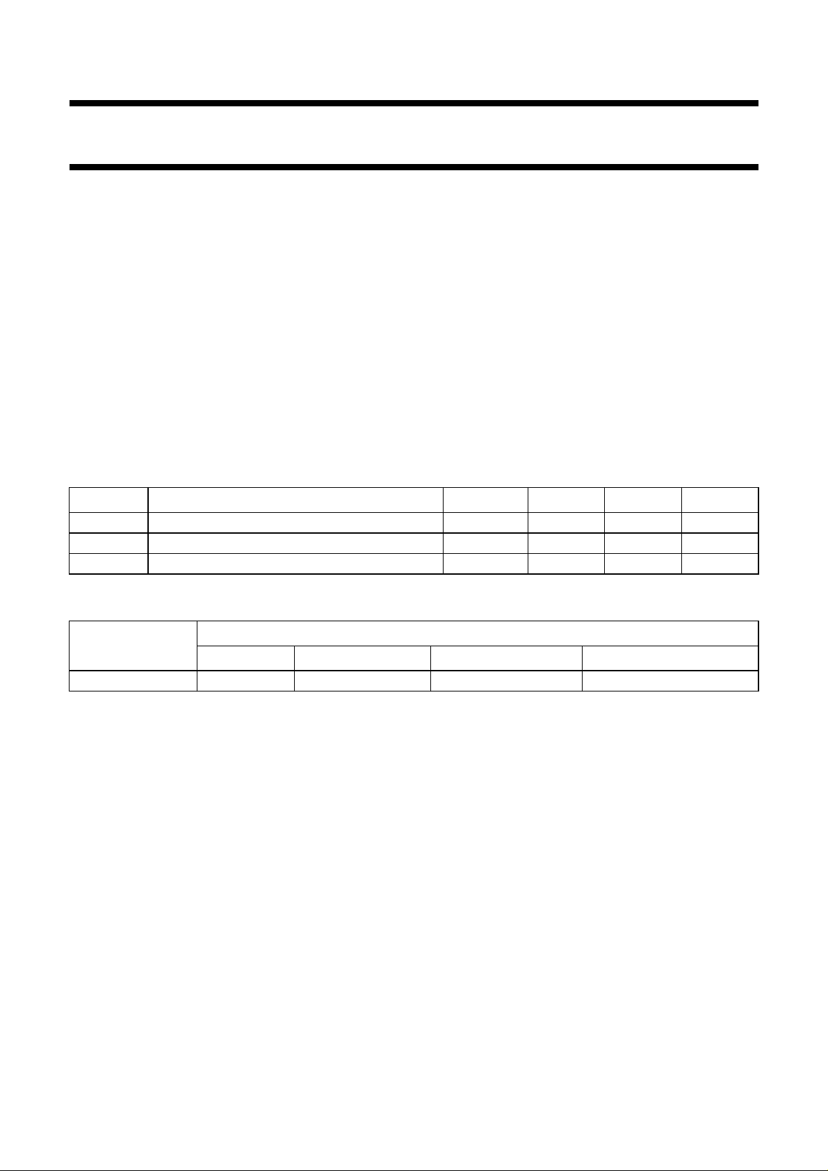
Instead of potentiometers at EQ AMP
fixed resistors may be used. The value
depends on applied heads.
TEA0677T
Fig.1 Block and application diagram.
Page 4
Philips Semiconductors Product specification
Dual pre-amplifier and equalizer for
reverse tape decks
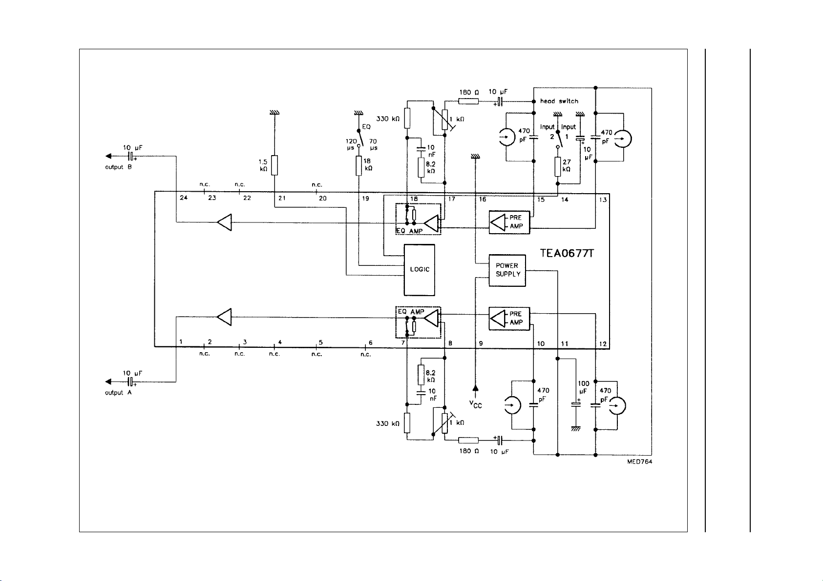
PINNING
SYMBOL PIN DESCRIPTION
OUTA 1 output channel A
n.c. 2 not connected
n.c. 3 not connected
n.c. 4 not connected
n.c. 5 not connected
n.c. 6 not connected
EQA 7 equalizing output channel A
EQFA 8 equalizing input channel A
V
CC
INA1 10 input channel A1 (forward or
V
REF
INA2 12 input channel A2 (reverse or
INB2 13 input channel B2 (reverse or
HS 14 head switch input
INB1 15 input channel B1 (forward or
GND 16 ground
EQFB 17 equalizing input channel B
EQB 18 equalizing output channel B
EQS 19 equalizing switch input
n.c. 20 not connected
ACUR 21 auxiliary current
n.c. 22 not connected
n.c. 23 not connected
OUTB 24 output channel B
9 supply voltage
reverse)
11 reference voltage
forward)
forward)
reverse)
TEA0677T
Fig.2 Pin configuration.
FUNCTIONAL DESCRIPTION
Head switching is achieved when pin 14 (HS) is
connected to GND via a 27 kΩ resistor (inputs INA2, INB2
active), or left open-circuit (inputs INA1, INB1 active).
The 10 µF capacitor at pin 14 sets the time constant for
smooth switching.
August 1993 4
Time constant switching for equalization
(70 µs/120 µs) is achieved when pin 19 (EQS) is
connected to ground via an 18 kΩ resistor (120µs) or left
open-circuit (70 µs).
Page 5

Philips Semiconductors Product specification
Dual pre-amplifier and equalizer for
TEA0677T
reverse tape decks
LIMITING VALUES
In accordance with the Absolute Maximum Rating System (IEC134).
SYMBOL PARAMETER MIN. MAX. UNIT
V
CC
V
I
t
short
T
amb
T
stg
T
s
V
es
Note to the Limiting values
1. Classification A: human body model; C = 100 pF, R = 1.5 kΩ, V ≥ 2 kV; charge device model; C = 200 pF, R = 0 Ω,
V ≥ 500 V.
CHARACTERISTICS
= 10 V; f = 20 Hz to 20 kHz; T
V
CC
EQ switch in the 70 µs position; unless otherwise specified.
DC supply voltage 0 16 V
input voltage (pin 1 to 24) except pin 11 (V
pin 11 (V
) to VCCshort-circuiting duration − 5s
REF
REF
) to V
CC
−0.3 V
CC
V
operating ambient temperature −40 +85 °C
storage temperature −65 +150 °C
soldering temperature (wave solder for 10 s at lead) − 260 °C
electrostatic handling (note 1) −−−
= +25 °C; all levels are referenced to 387.5 mV (RMS; 0 dB) at output; see Fig.1;
amb
SYMBOL PARAMETER CONDITIONS MIN. TYP. MAX. UNIT
V
CC
I
CC
supply voltage 7.6 10 12 V
supply current pins 10, 12, 13 and 15 − 23 26 mA
connected to V
REF
channel matching f = 1 kHz; VO= 0 dB −0.5 − +0.5 dB
THD total harmonic distortion 2nd and 3rd f = 1 kHz; V
harmonic f = 10 kHz; V
head room at output V
= 7.6 V; 12 14 − dB
CC
= 0 dB − 0.04 0.1 %
O
= 6 dB − 0.08 0.15 %
O
THD = 1%; f = 1 kHz
PSRR power supply ripple rejection 0.25 V (RMS); 45 50 − dB
f = 1 kHz; see Fig.3
α
CS
channel separation f = 1 kHz; VO= +10 dB; 64 70 − dB
see Fig.4
α
CC
crosstalk between active and inactive
f = 1 kHz; VO= +10 dB 70 77 − dB
input
R
Lmin
minimum load resistance at output f = 1 kHz; VO= 12 dB; 10 −−kΩ
THD = 1%
G
v
voltage gain (pre-amplifier) from input
f = 1 kHz 29 30 31 dB
pins 10, 12, 13 and 15 to pin EQF
V
off
I
B
R
EQ
R
I
input offset voltage − 2 − mV
input bias current − 0.1 0.4 µA
equalizing resistor 4.7 5.8 6.9 kΩ
input resistance head inputs 60 100 − kΩ
August 1993 5
Page 6

Philips Semiconductors Product specification
Dual pre-amplifier and equalizer for
TEA0677T
reverse tape decks
SYMBOL PARAMETER CONDITIONS MIN. TYP. MAX. UNIT
A
V
N equivalent noise voltage input unweighted; − 0.7 1.4 µV
(S+N)/N signal-plus-noise to noise ratio internal gain 40 dB
I
OGND
I
OVCC
Z
O
Switching thresholds
Equalization (pin 19)
V
EQS
I
EQ70
I
EQ120
Head switch (pin 14)
V
IN1
I
IN1
V
IN2
I
IN2
Note to the characteristics
1. For an application with a fixed EQ time constant of 120 µs the equalizing network may be applied completely
external. In this application the 8.2 kΩ resistor has to be changed to 14 kΩ and the internal resistor REQ = 5.8 kΩ
must be short-circuited by fixing the EQ-switch input at the 70 µs position (pin 19; EQS left open-circuit). To activate
the inputs INA1 and INB1 pin 10 (HS) may be left open-circuit. In this event the DC level at pin 10 (HS) is 0.775 VCC.
open-loop gain
pins INA1/INA2 to pin OUTA f = 10 kHz 80 86 − dB
pins INB1/INB2 to pin OUTB f = 400 Hz 104 110 − dB
(RMS value) 20 Hz to 20 kHz;
R
source
= 0 Ω
68 74 − dB
linear;
CCIR/ARM weighted;
see Fig.4
DC output voltage; pins 1 (OUTA) reference to V
REF;
−− ±0.15 V
and 16 (OUTB) tape head DC coupled
DC output current capability to ground −2 −−mA
DC output current capability to V
CC
300 −−µA
output impedance − 80 100 Ω
voltage at pin EQS −− 5V
70 µs input current −− −150 µA
120 µs input current −250 −−1000 µA
inputs INA1 and INB1 active note 1 0.65VCC0.775VCC1.0V
CC
V
maximum input current −150 90 150 µA
inputs INA2 and INB2 active 0.1V
0.225VCC0.35VCCV
CC
maximum input current −50 −90 −150 µA
General note
It is recommended to switch off V
with a gradient of 400 V/s at maximum to avoid plops on tape in the event of contact
CC
between tape and tape head while switching off.
August 1993 6
Page 7

This text is here in white to force landscape pages to be rotated correctly when browsing through the pdf in the Acrobat reader.This text is here in
_white to force landscape pages to be rotated correctly when browsing through the pdf in the Acrobat reader.This text is here inThis text is here in
white to force landscape pages to be rotated correctly when browsing through the pdf in the Acrobat reader. white to force landscape pages to be ...
August 1993 7
Philips Semiconductors Product specification
Dual pre-amplifier and equalizer for
reverse tape decks
Fig.3 Test circuit for power supply ripple rejection.
TEA0677T
Page 8

This text is here in white to force landscape pages to be rotated correctly when browsing through the pdf in the Acrobat reader.This text is here in
_white to force landscape pages to be rotated correctly when browsing through the pdf in the Acrobat reader.This text is here inThis text is here in
white to force landscape pages to be rotated correctly when browsing through the pdf in the Acrobat reader. white to force landscape pages to be ...
August 1993 8
Philips Semiconductors Product specification
Dual pre-amplifier and equalizer for
reverse tape decks
Fig.4 Test circuit for channel separation and signal-to-noise ratio.
TEA0677T
Page 9

Philips Semiconductors Product specification
Dual pre-amplifier and equalizer for
reverse tape decks
TEA0677T
Fig.5 PCB layout example.
August 1993 9
Page 10

Philips Semiconductors Product specification
Dual pre-amplifier and equalizer for
reverse tape decks
Table 1 Component list pcb layout example.
COMPONENT VALUE
R1, R11 270 kΩ
R2, R12 180 kΩ
R3, R13, R20 1.5 kΩ
R4, R14 24 kΩ
R5, R15 8.2 kΩ
R6, R16 330 kΩ
R7, R17 1 kΩ
R8, R18 0.18 kΩ
R9 68 kΩ to 1000 kΩ
R10 27 kΩ
R19 18 kΩ
R21, R22 0 kΩ
C1, C11, C7, C17, C20 10 µF
C2, C12 330 nF
C3, C13 100 nF
C4, C14 15 nF
C5, C15 4.7 nF
C6, C16 10 nF
C8, C9, C18, C19 0.47 nF
C10 100 µF
TEA0677T
August 1993 10
Page 11

Philips Semiconductors Product specification
Dual pre-amplifier and equalizer for
reverse tape decks
PACKAGE OUTLINE
SO24: plastic small outline package; 24 leads; body width 7.5 mm
D
c
y
Z
24
13
TEA0677T
SOT137-1
E
H
E
A
X
v M
A
pin 1 index
1
e
0 5 10 mm
DIMENSIONS (inch dimensions are derived from the original mm dimensions)
mm
A
max.
2.65
0.10
A1A2A
0.30
2.45
0.10
2.25
0.012
0.096
0.004
0.089
0.25
0.01
b
3
p
0.49
0.32
0.36
0.23
0.019
0.013
0.014
0.009
UNIT
inches
Note
1. Plastic or metal protrusions of 0.15 mm maximum per side are not included.
(1)E(1) (1)
cD
15.6
15.2
0.61
0.60
12
w M
b
p
scale
eHELLpQ
7.6
1.27
7.4
0.30
0.050
0.29
10.65
10.00
0.419
0.394
A
1.4
0.055
Q
2
A
1
detail X
1.1
1.1
0.4
0.043
0.016
1.0
0.043
0.039
0.25
0.01
L
p
L
(A )
0.25 0.1
0.01
A
3
θ
ywv θ
Z
0.9
0.4
0.035
0.004
0.016
o
8
o
0
OUTLINE
VERSION
SOT137-1
IEC JEDEC EIAJ
075E05 MS-013AD
REFERENCES
August 1993 11
EUROPEAN
PROJECTION
ISSUE DATE
95-01-24
97-05-22
Page 12

Philips Semiconductors Product specification
Dual pre-amplifier and equalizer for
reverse tape decks
SOLDERING
Introduction
There is no soldering method that is ideal for all IC
packages. Wave soldering is often preferred when
through-hole and surface mounted components are mixed
on one printed-circuit board. However, wave soldering is
not always suitable for surface mounted ICs, or for
printed-circuits with high population densities. In these
situations reflow soldering is often used.
This text gives a very brief insight to a complex technology.
A more in-depth account of soldering ICs can be found in
our
“IC Package Databook”
Reflow soldering
Reflow soldering techniques are suitable for all SO
packages.
Reflow soldering requires solder paste (a suspension of
fine solder particles, flux and binding agent) to be applied
to the printed-circuit board by screen printing, stencilling or
pressure-syringe dispensing before package placement.
Several techniques exist for reflowing; for example,
thermal conduction by heated belt. Dwell times vary
between 50 and 300 seconds depending on heating
method. Typical reflow temperatures range from
215 to 250 °C.
Preheating is necessary to dry the paste and evaporate
the binding agent. Preheating duration: 45 minutes at
45 °C.
(order code 9398 652 90011).
TEA0677T
Wave soldering
Wave soldering techniques can be used for all SO
packages if the following conditions are observed:
• A double-wave (a turbulent wave with high upward
pressure followed by a smooth laminar wave) soldering
technique should be used.
• The longitudinal axis of the package footprint must be
parallel to the solder flow.
• The package footprint must incorporate solder thieves at
the downstream end.
During placement and before soldering, the package must
be fixed with a droplet of adhesive. The adhesive can be
applied by screen printing, pin transfer or syringe
dispensing. The package can be soldered after the
adhesive is cured.
Maximum permissible solder temperature is 260 °C, and
maximum duration of package immersion in solder is
10 seconds, if cooled to less than 150 °C within
6 seconds. Typical dwell time is 4 seconds at 250 °C.
A mildly-activated flux will eliminate the need for removal
of corrosive residues in most applications.
Repairing soldered joints
Fix the component by first soldering two diagonallyopposite end leads. Use only a low voltage soldering iron
(less than 24 V) applied to the flat part of the lead. Contact
time must be limited to 10 seconds at up to 300 °C. When
using a dedicated tool, all other leads can be soldered in
one operation within 2 to 5 seconds between
270 and 320 °C.
August 1993 12
Page 13

Philips Semiconductors Product specification
Dual pre-amplifier and equalizer for
TEA0677T
reverse tape decks
DEFINITIONS
Data sheet status
Objective specification This data sheet contains target or goal specifications for product development.
Preliminary specification This data sheet contains preliminary data; supplementary data may be published later.
Product specification This data sheet contains final product specifications.
Limiting values
Limiting values given are in accordance with the Absolute Maximum Rating System (IEC 134). Stress above one or
more of the limiting values may cause permanent damage to the device. These are stress ratings only and operation
of the device at these or at any other conditions above those given in the Characteristics sections of the specification
is not implied. Exposure to limiting values for extended periods may affect device reliability.
Application information
Where application information is given, it is advisory and does not form part of the specification.
LIFE SUPPORT APPLICATIONS
These products are not designed for use in life support appliances, devices, or systems where malfunction of these
products can reasonably be expected to result in personal injury. Philips customers using or selling these products for
use in such applications do so at their own risk and agree to fully indemnify Philips for any damages resulting from such
improper use or sale.
August 1993 13
 Loading...