

Page 1

INTEGRATED CIRCUITS
DATA SH EET
TEA0676T
Dual pre-amplifier and equalizer for
reverse tape decks
Product specification
Supersedes data of 1996 Jun 20
File under Integrated Circuits, IC01
1997 Oct 07
Page 2

Philips Semiconductors Product specification
Dual pre-amplifier and equalizer for
TEA0676T
reverse tape decks
FEATURES
• Dual head pre-amplifiers
• Reverse head switching
• Equalization with electronically switched time constants
• Output level like Dolby level of 387.5 mV = 0 dB
• Improved EMC behaviour.
QUICK REFERENCE DATA
SYMBOL PARAMETER CONDITIONS MIN. TYP. MAX. UNIT
V
CC
I
CC
SN+
-------------N
V
o (rms)
supply voltage 7.6 10 12 V
supply current VCC=10V − 10 13 mA
signal plus noise-to-noise ratio unweighted RMS value 67 73 − dB
output voltage (0 dB) (RMS value) gain internal = 40 dB; linear − 387.5 − mV
GENERAL DESCRIPTION
The TEA0676T is a monolithic bipolar integrated circuit
intended for applications in car radios. It includes head and
equalization amplifiers with electronically switchable time
constants. Furthermore it includes electronically
switchable inputs for tape drivers with reverse heads.
The device will operate with power supplies in a range of
7.6 to 12.0 V. The output overload level increases with the
increase in supply voltage, so it is advisable to use a
regulated power supply or a supply with a long time
constant.
ORDERING INFORMATION
TYPE
NUMBER
TEA0676T SO16 plastic small outline package; 16 leads; body width 7.5 mm SOT162-1
NAME DESCRIPTION VERSION
PACKAGE
1997 Oct 07 2
Page 3
Philips Semiconductors Product specification
Dual pre-amplifier and equalizer for
reverse tape decks
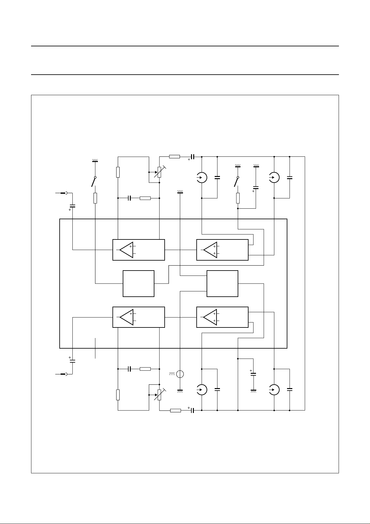
BLOCK DIAGRAM
handbook, full pagewidth
equalizer
switch
70 µs
10 µF
OUTB
16
120 µs
18 kΩ
EQSW
15
330 kΩ
10 nF
EQOUTB
14
8.2 kΩ
180 Ω
1 kΩ
EQINB
13
GND
12
10 µF
INB1
11
470
pF
head
switch
IN1
IN2
27 kΩ
HSW INB2
10
10
µF
TEA0676T
470
pF
9
TEA0676T
1
OUT A
10 µF
2
n.c.
LOGIC
3
EQOUT A
10 nF
330 kΩ
EQ
AMPLIFIER
EQ
AMPLIFIER
8.2 kΩ
4
EQINA
1 kΩ
180 Ω
5
V
CC
10 V
10 µF
INA1
PREAMPLIFIER
POWER
SUPPLY
PREAMPLIFIER
470
pF
µF
8
INA2
470
pF
MGE862
76
V
ref
100
Fig.1 Block and application diagram.
1997 Oct 07 3
Page 4
Philips Semiconductors Product specification
Dual pre-amplifier and equalizer for
reverse tape decks
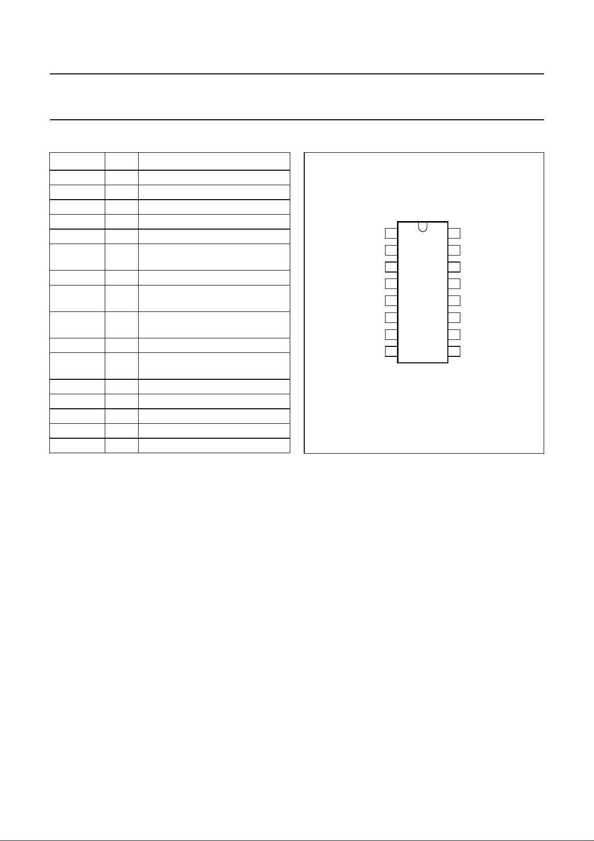
PINNING
SYMBOL PIN DESCRIPTION
OUTA 1 output channel A
n.c. 2 not connected
EQOUTA 3 output equalizer channel A
EQINA 4 input equalizer channel A
V
CC
INA1 6 input channel A1
V
ref
INA2 8 input channel A2
INB2 9 input channel B2
HSW 10 input head switch
INB1 11 input channel B1
GND 12 ground
EQINB 13 input equalizer channel B
EQOUTB 14 output equalizer channel B
EQSW 15 input equalizer switch
OUTB 16 output channel B
5 supply voltage
(forward or reverse)
7 reference voltage
(reverse or forward)
(reverse or forward)
(forward or reverse)
handbook, halfpage
EQOUTA
OUTA
1
n.c.
2
3
V
CC
INA1
V
ref
INA2
4
TEA0676T
5
6
7
8
MGE861
EQINA
Fig.2 Pin configuration.
TEA0676T
16
OUTB
15
EQSW
14
EQOUTB
13
EQINB
12
GND
11
INB1
10
HSW
9
INB2
FUNCTIONAL DESCRIPTION
Gain of pre-amplifier = 30 dB; minimum gain of
EQ-amplifier = 24.5 dB at f = 1 kHz with 70 µs cut-off
frequency.
Head switching is achieved when pin 10 (HSW) is
connected to ground via a 27 kΩ resistor (inputs INA2,
INB2 are active) or connected to HIGH level (0.8V
CC
)
(inputs INA1, INB1 are active).
Equalization time constant switching (70 µs/120 µs) is
achieved when pin 15 (EQSW) is connected to ground via
an 18 kΩ resistor (120 µs) or left open-circuit (70 µs).
1997 Oct 07 4
Page 5
Philips Semiconductors Product specification
Dual pre-amplifier and equalizer for
TEA0676T
reverse tape decks
LIMITING VALUES
In accordance with the Absolute Maximum Rating System (IEC 134).
SYMBOL PARAMETER CONDITIONS MIN. MAX. UNIT
V
CC
∆V
(12-x)
T
stg
T
amb
V
es
Notes
1. Human body model: C = 100 pF; R = 1.5 kΩ.
2. Machine model: C = 200 pF; R = 0 Ω.
THERMAL CHARACTERISTICS
SYMBOL PARAMETER VALUE UNIT
R
th j-a
supply voltage 0 14 V
voltage at pins 1 to 11, 13 to 16 with respect to pin 12 0 V
CC
V
storage temperature −55 +150 °C
operating ambient temperature −40 +85 °C
electrostatic handling voltage note 1 −2000 +2000 V
note 2 −500 +500 V
thermal resistance from junction to ambient in free air 70 K/W
1997 Oct 07 5
Page 6

Philips Semiconductors Product specification
Dual pre-amplifier and equalizer for
TEA0676T
reverse tape decks
CHARACTERISTICS
V
= 10 V; RL=10kΩ; CL= 2.5 nF; T
CC
387.5 mV with 0 dB as standard; EQ switch in 70 µs position; unless otherwise specified; see notes 1 and 2.
SYMBOL PARAMETER CONDITIONS MIN. TYP. MAX. UNIT
Supply
V
CC
I
CC
supply voltage (pin 5) 7.6 10.0 12.0 V
supply current − 10 13 mA
THD total harmonic distortion f = 1 kHz; V
H
R
headroom at output VCC= 7.6 V; THD = 1%;
PSRR power supply ripple
rejection
α
cs
α
m
α
ct
channel separation selective measurement;
channel matching selective measurement;
crosstalk between active
and inactive input
SN+
-------------N
V
no(rms)
signal plus noise-to-noise
ratio (RMS value)
equivalent input noise
voltage (RMS value)
G
v
voltage gain of
pre-amplifier
A
v
R
EQ
Z
I
open-loop amplification pin INA1 to pin OUTA and
equalization resistor 4.7 5.8 6.9 kΩ
input impedance
pre-amplifier
Z
O
output impedance
EQ-amplifier
R
L
C
L
V
offset(DC)
I
O(GND)
I
O(VCC)
output load resistance 10 −− kΩ
output load capacitance 0 − 10 nF
input offset voltage pins INA1, INA2, INB1 and
DC current capability output to ground −2 −− mA
DC current capability output to V
EMC DC offset voltage at
pins 1 and 16
=25°C; Vo= 0 dB means 387.5 mV at output; all levels are referenced to
amb
=0dB − 0.08 0.15 %
o
f = 10 kHz; V
=6dB − 0.15 0.3 %
o
12 −− dB
f=1kHz
V
< 0.25 V; f = 1 kHz − 50 − dB
R(rms)
57 63 − dB
f = 1 kHz; Vo=10dB
−0.5 − +0.5 dB
f = 1 kHz; Vo=0dB
selective measurement;
70 77 − dB
f = 1 kHz; Vo=10dB
unweighted;
f = 20 Hz to 20 kHz; R
=0Ω;
s
67 73 − dB
internal gain 40 dB; linear;
see Fig.13
unweighted;
− 0.8 −µV
f = 20 Hz to 20 kHz; Rs=0Ω
from pin INA1 or INA2 to
29 30 31 dB
pin EQINA and from pin INB1
or INB2 to pin EQINB
pin INB1 to pin OUTB
f = 10 kHz 80 86 − dB
f = 400 Hz 104 110 − dB
60 100 − kΩ
− 80 100 Ω
− 2 − mV
INB2 connected to V
CC
f = 900 MHz; V
ref
= 6 V (RMS);
i
300 −− µA
− 50 − mV
see Figs 12, 14 and 15
1997 Oct 07 6
Page 7

Philips Semiconductors Product specification
Dual pre-amplifier and equalizer for
TEA0676T
reverse tape decks
SYMBOL PARAMETER CONDITIONS MIN. TYP. MAX. UNIT
Switching thresholds
E
QUALIZATION TIME CONSTANT SWITCHING
V
EQSW
I
EQSW
V
EQSW(HIGH)
V
EQSW(LOW)
HEAD SWITCHING
V
HSW
I
HSW
V
HSW(HIGH)
V
HSW(LOW)
Notes
1. For an application with a fixed equalization time constant of 120 µs the equalizing network may be applied completely
external. In this application the 8.2 kΩ resistor has to be changed to 14 kΩ and the internal resistor REQ= 5.8 kΩ
must be short-circuited by fixing the equalization switch input at 70 µs (pin 15 left open-circuit). To activate the inputs
INA1 and INB1, pin 10 (HSW) might be left open-circuit. In this event the DC level at pin 10 (HSW) is 0.8V
2. It is recommended to switch off VCC with a gradient of 400 V/s at maximum to avoid plops on the tape in the event
of contact between tape and tape head while switching off.
pin voltage load current +100 to −100 µA − 0.8VCC− V
input current V
pin voltage time constant 70 µs active
pin voltage time constant 120 µs active 0 −
EQSW
= 0 to V
CC
−180 − +180 µA
1
⁄2VCC+ 0.5 − V
CC
1
⁄2VCC− 0.5 V
pin voltage load current +90 to −90 µA − 0.8VCC− V
input current V
HIGH-level pin voltage inputs INA1 and INB1 active
LOW-level pin voltage inputs INA2 and INB2 active 0 −
HSW
= 0 to V
CC
−170 − +170 µA
1
⁄2VCC+ 0.5 − V
CC
1
⁄2VCC− 0.5 V
CC
V
V
1997 Oct 07 7
Page 8

Philips Semiconductors Product specification
Dual pre-amplifier and equalizer for
reverse tape decks
INTERNAL PIN CONFIGURATIONS
handbook, halfpage
+
100
Ω
1
5 V
80 Ω
MGE863
handbook, halfpage
TEA0676T
5.8
kΩ
3
5 V
MGE864
+
80 Ω
100
Ω
Fig.3 Pins 1 and 16: output channel.
handbook, halfpage
Fig.4 Pins 3 and 14: equalizer outputs.
MGE865
4
10 kΩ
1 pF
handbook, halfpage
5
MGE866
+
Fig.5 Pins 4 and 13: equalizer inputs.
1997 Oct 07 8
Fig.6 Pin 5: supply voltage.
Page 9

Philips Semiconductors Product specification
Dual pre-amplifier and equalizer for
reverse tape decks
handbook, halfpage
6
5 V
100 kΩ
5 V
220 Ω
12
pF
+
MGE867
handbook, halfpage
TEA0676T
+
2.5 kΩ
5 V
7
2.5 kΩ
MGE868
Fig.7 Pins 6, 8, 9, 11: input channel.
handbook, halfpage
Fig.8 Pin 7: reference voltage.
10
8 V
+
MGE869
handbook, halfpage
15
8 V
+
MGE870
Fig.9 Pin 10: input head switch.
1997 Oct 07 9
Fig.10 Pin 15: input equalizer switch.
Page 10

Philips Semiconductors Product specification
Dual pre-amplifier and equalizer for
reverse tape decks
TEST AND APPLICATION INFORMATION
handbook, full pagewidth
10 kΩ
equalizer
switch
70 µs
10 µF
OUTB
16
120 µs
18 kΩ
EQSW
15
330 kΩ
10 nF
EQOUTB
14
8.2 kΩ
180 Ω
1 kΩ
EQINB
13
GND
12
10 µF
200 Ω
INB1
11
10
µF
470
head
pF
switch
IN1
IN2
27 kΩ
HSW INB2
10
10
µF
TEA0676T
470
pF
10
200 Ω
µF
9
10 kΩ
TEA0676T
1
OUT A
10 µF
2
n.c.
LOGIC
3
EQOUT A
10 nF
330 kΩ
EQ
AMPLIFIER
EQ
AMPLIFIER
8.2 kΩ
4
EQINA
1 kΩ
180 Ω
5
V
CC
10 V
200 Ω
10 µF
INA1
PREAMPLIFIER
POWER
SUPPLY
PREAMPLIFIER
10
µF
470
pF
µF
8
INA2
10
µF
200 Ω
470
pF
MGE871
76
V
ref
100
Fig.11 Test circuit.
1997 Oct 07 10
Page 11

Philips Semiconductors Product specification
Dual pre-amplifier and equalizer for
reverse tape decks
handbook, full pagewidth
20 kΩ
10 µF
OUTB
16
EQSW
15
EQOUTB
14
EQ
AMPLIFIER
EQINB
13
10 kΩ
GND
12
200 Ω
INB1
11
470
pF
PREAMPLIFIER
head
switch
IN1
IN2
27 kΩ
HSW INB2
10
200 Ω
10
µF
TEA0676T
470
pF
9
TEA0676T
1
OUT A
10 µF
2
n.c.
LOGIC
3
EQOUT A
EQ
AMPLIFIER
20 kΩ
10 kΩ
4
EQINA
5
V
CC
10 V
200 Ω
INA1
POWER
SUPPLY
PREAMPLIFIER
470
pF
10 Ω
µF
200 Ω
8
INA2
470
pF
f = 900 MHz
Vi = 6 V (RMS)
MGE872
76
V
ref
100
40 Ω
Fig.12 EMC test diagram.
1997 Oct 07 11
Page 12

Philips Semiconductors Product specification
Dual pre-amplifier and equalizer for
reverse tape decks
handbook, full pagewidth
equalizer
switch
70 µs
10 µF
OUTB
16
120 µs
18 kΩ
EQSW
15
EQOUTB
14
10 kΩ
20 kΩ
EQINB
13
EQ
AMPLIFIER
GND
12
INB1
11
head
switch
IN1
IN2
27 kΩ
HSW INB2
10
PREAMPLIFIER
10
µF
TEA0676T
9
TEA0676T
1
OUT A
10 µF
2
n.c.
LOGIC
3
EQOUT A
EQ
AMPLIFIER
20 kΩ
10 kΩ
4
EQINA
POWER
SUPPLY
PREAMPLIFIER
5
V
CC
INA1
10 V
76
V
ref
100
8
INA2
µF
MGE873
Fig.13 Noise test diagram.
1997 Oct 07 12
Page 13

Philips Semiconductors Product specification
Dual pre-amplifier and equalizer for
reverse tape decks
LAYOUT OF PRINTED CIRCUIT BOARD FOR EMC TEST CIRCUIT
handbook, full pagewidth
50
54
TEA0676T
27 kΩ 200 Ω
200 Ω
470 pF
0 Ω 0 Ω
100 nF
40 Ω
10 Ω
470 pF
200 Ω
TEA0676T
0 Ω
Fig.14 Top side with components.
1997 Oct 07 13
0 Ω
470 pF
10 kΩ
20 kΩ
20 kΩ
10 kΩ
470 pF
200 Ω
100 nF
MBH457
Page 14

Philips Semiconductors Product specification
Dual pre-amplifier and equalizer for
reverse tape decks
handbook, full pagewidth
50
TEA0676T
54
X3
10 µF
S1
MP
100 µF 100 µF
MP
HFDR.
MP
10 µF
10 µF
X2
X1
Fig.15 Bottom side with components.
X4
MBH458
1997 Oct 07 14
Page 15

Philips Semiconductors Product specification
Dual pre-amplifier and equalizer for
reverse tape decks
PACKAGE OUTLINE
SO16: plastic small outline package; 16 leads; body width 7.5 mm
D
c
y
Z
16
9
TEA0676T
SOT162-1
E
H
E
A
X
v M
A
pin 1 index
1
e
DIMENSIONS (inch dimensions are derived from the original mm dimensions)
mm
A
max.
2.65
0.10
A
1
0.30
0.10
0.012
0.004
A2A
2.45
2.25
0.096
0.089
0.25
0.01
b
3
p
0.49
0.32
0.36
0.23
0.019
0.013
0.014
0.009
UNIT
inches
Note
1. Plastic or metal protrusions of 0.15 mm maximum per side are not included.
8
w M
b
p
0 5 10 mm
scale
(1)E(1) (1)
cD
10.5
10.1
0.41
0.40
eHELLpQ
7.6
1.27
7.4
0.30
0.050
0.29
A
2
10.65
10.00
0.419
0.394
A
1
1.4
0.055
1.1
0.4
0.043
0.016
detail X
0.043
0.039
1.1
1.0
Q
3
0.25 0.1
0.01
A
θ
ywv θ
0.004
Z
0.9
0.4
0.035
0.016
o
8
o
0
(A )
L
p
L
0.25
0.01
OUTLINE
VERSION
SOT162-1
IEC JEDEC EIAJ
075E03 MS-013AA
REFERENCES
1997 Oct 07 15
EUROPEAN
PROJECTION
ISSUE DATE
95-01-24
97-05-22
Page 16

Philips Semiconductors Product specification
Dual pre-amplifier and equalizer for
reverse tape decks
SOLDERING
Introduction
There is no soldering method that is ideal for all IC
packages. Wave soldering is often preferred when
through-hole and surface mounted components are mixed
on one printed-circuit board. However, wave soldering is
not always suitable for surface mounted ICs, or for
printed-circuits with high population densities. In these
situations reflow soldering is often used.
This text gives a very brief insight to a complex technology.
A more in-depth account of soldering ICs can be found in
our
“IC Package Databook”
Reflow soldering
Reflow soldering techniques are suitable for all SO
packages.
Reflow soldering requires solder paste (a suspension of
fine solder particles, flux and binding agent) to be applied
to the printed-circuit board by screen printing, stencilling or
pressure-syringe dispensing before package placement.
Several techniques exist for reflowing; for example,
thermal conduction by heated belt. Dwell times vary
between 50 and 300 seconds depending on heating
method. Typical reflow temperatures range from
215 to 250 °C.
Preheating is necessary to dry the paste and evaporate
the binding agent. Preheating duration: 45 minutes at
45 °C.
(order code 9398 652 90011).
TEA0676T
Wave soldering
Wave soldering techniques can be used for all SO
packages if the following conditions are observed:
• A double-wave (a turbulent wave with high upward
pressure followed by a smooth laminar wave) soldering
technique should be used.
• The longitudinal axis of the package footprint must be
parallel to the solder flow.
• The package footprint must incorporate solder thieves at
the downstream end.
During placement and before soldering, the package must
be fixed with a droplet of adhesive. The adhesive can be
applied by screen printing, pin transfer or syringe
dispensing. The package can be soldered after the
adhesive is cured.
Maximum permissible solder temperature is 260 °C, and
maximum duration of package immersion in solder is
10 seconds, if cooled to less than 150 °C within
6 seconds. Typical dwell time is 4 seconds at 250 °C.
A mildly-activated flux will eliminate the need for removal
of corrosive residues in most applications.
Repairing soldered joints
Fix the component by first soldering two diagonallyopposite end leads. Use only a low voltage soldering iron
(less than 24 V) applied to the flat part of the lead. Contact
time must be limited to 10 seconds at up to 300 °C. When
using a dedicated tool, all other leads can be soldered in
one operation within 2 to 5 seconds between
270 and 320 °C.
1997 Oct 07 16
Page 17

Philips Semiconductors Product specification
Dual pre-amplifier and equalizer for
TEA0676T
reverse tape decks
DEFINITIONS
Data sheet status
Objective specification This data sheet contains target or goal specifications for product development.
Preliminary specification This data sheet contains preliminary data; supplementary data may be published later.
Product specification This data sheet contains final product specifications.
Limiting values
Limiting values given are in accordance with the Absolute Maximum Rating System (IEC 134). Stress above one or
more of the limiting values may cause permanent damage to the device. These are stress ratings only and operation
of the device at these or at any other conditions above those given in the Characteristics sections of the specification
is not implied. Exposure to limiting values for extended periods may affect device reliability.
Application information
Where application information is given, it is advisory and does not form part of the specification.
LIFE SUPPORT APPLICATIONS
These products are not designed for use in life support appliances, devices, or systems where malfunction of these
products can reasonably be expected to result in personal injury. Philips customers using or selling these products for
use in such applications do so at their own risk and agree to fully indemnify Philips for any damages resulting from such
improper use or sale.
1997 Oct 07 17
Page 18

Philips Semiconductors Product specification
Dual pre-amplifier and equalizer for
reverse tape decks
TEA0676T
NOTES
1997 Oct 07 18
Page 19

Philips Semiconductors Product specification
Dual pre-amplifier and equalizer for
reverse tape decks
TEA0676T
NOTES
1997 Oct 07 19
Page 20

Philips Semiconductors – a worldwide company
Argentina: see South America
Australia: 34 Waterloo Road, NORTH RYDE, NSW 2113,
Tel. +61 2 9805 4455, Fax. +61 2 98054466
Austria: Computerstr. 6, A-1101 WIEN, P.O. Box 213, Tel. +43 160 1010,
Fax. +43 160 101 1210
Belarus: Hotel Minsk Business Center, Bld. 3, r. 1211, Volodarski Str. 6,
220050 MINSK, Tel. +375 172 200 733, Fax. +375 172200 773
Belgium: see The Netherlands
Brazil: seeSouth America
Bulgaria: Philips Bulgaria Ltd., Energoproject, 15thfloor,
51 James Bourchier Blvd., 1407 SOFIA,
Tel. +359 2 689 211, Fax. +359 2 689102
Canada: PHILIPS SEMICONDUCTORS/COMPONENTS,
Tel. +1 800 234 7381
China/Hong Kong: 501 Hong Kong Industrial Technology Centre,
72 Tat Chee Avenue, Kowloon Tong, HONG KONG,
Tel. +852 2319 7888, Fax. +852 2319 7700
Colombia: see South America
Czech Republic: see Austria
Denmark: Prags Boulevard 80, PB 1919, DK-2300 COPENHAGEN S,
Tel. +45 32 88 2636, Fax. +45 31 570044
Finland: Sinikalliontie 3, FIN-02630 ESPOO,
Tel. +358 9 615800, Fax. +358 9 61580920
France: 4 Rue du Port-aux-Vins, BP317, 92156 SURESNES Cedex,
Tel. +33 1 40 99 6161, Fax. +33 140 99 6427
Germany: Hammerbrookstraße 69, D-20097 HAMBURG,
Tel. +49 40 23 53 60, Fax. +49 4023 536 300
Greece: No. 15, 25th March Street, GR 17778 TAVROS/ATHENS,
Tel. +30 1 4894 339/239, Fax. +30 1 4814240
Hungary: seeAustria
India: Philips INDIA Ltd, Band Box Building, 2nd floor,
254-D, Dr. Annie Besant Road, Worli, MUMBAI 400 025,
Tel. +91 22 493 8541, Fax. +91 22 4930966
Indonesia: see Singapore
Ireland: Newstead, Clonskeagh, DUBLIN 14,
Tel. +353 1 7640 000, Fax. +353 1 7640200
Israel: RAPAC Electronics, 7 Kehilat Saloniki St, PO Box 18053,
TEL AVIV 61180, Tel. +972 3 645 0444, Fax. +9723 649 1007
Italy: PHILIPS SEMICONDUCTORS, Piazza IV Novembre 3,
20124 MILANO, Tel. +39 2 6752 2531, Fax. +39 26752 2557
Japan: Philips Bldg 13-37, Kohnan 2-chome, Minato-ku, TOKYO 108,
Tel. +81 3 3740 5130, Fax. +81 3 37405077
Korea: Philips House, 260-199 Itaewon-dong, Yongsan-ku, SEOUL,
Tel. +82 2 709 1412, Fax. +82 2 7091415
Malaysia: No. 76 Jalan Universiti, 46200 PETALING JAYA, SELANGOR,
Tel. +60 3 750 5214, Fax. +60 3 757 4880
Mexico: 5900 Gateway East, Suite 200, EL PASO, TEXAS 79905,
Tel. +9-5 800 234 7381
Middle East: see Italy
Netherlands: Postbus 90050, 5600 PB EINDHOVEN, Bldg. VB,
Tel. +31 40 27 82785, Fax. +31 40 2788399
New Zealand: 2 Wagener Place, C.P.O. Box 1041, AUCKLAND,
Tel. +64 9 849 4160, Fax. +64 9 8497811
Norway: Box 1, Manglerud 0612, OSLO,
Tel. +47 22 74 8000, Fax. +47 22 748341
Philippines: Philips Semiconductors Philippines Inc.,
106 Valero St. Salcedo Village, P.O. Box 2108 MCC, MAKATI,
Metro MANILA, Tel. +63 2 816 6380, Fax. +63 2817 3474
Poland: Ul. Lukiska 10, PL 04-123 WARSZAWA,
Tel. +48 22 612 2831, Fax. +48 22 6122327
Portugal: see Spain
Romania: see Italy
Russia: Philips Russia, Ul. Usatcheva 35A, 119048 MOSCOW,
Tel. +7 095 755 6918, Fax. +7 095 7556919
Singapore: Lorong 1, Toa Payoh, SINGAPORE 1231,
Tel. +65 350 2538, Fax. +65 251 6500
Slovakia: see Austria
Slovenia: see Italy
South Africa: S.A. PHILIPS Pty Ltd., 195-215 Main Road Martindale,
2092 JOHANNESBURG, P.O. Box 7430 Johannesburg 2000,
Tel. +27 11 470 5911, Fax. +27 11 4705494
South America: Rua do Rocio 220, 5th floor, Suite 51,
04552-903 São Paulo, SÃO PAULO - SP, Brazil,
Tel. +55 11 821 2333, Fax. +55 11 8291849
Spain: Balmes 22, 08007 BARCELONA,
Tel. +34 3 301 6312, Fax. +34 3 3014107
Sweden: Kottbygatan 7, Akalla, S-16485 STOCKHOLM,
Tel. +46 8 632 2000, Fax. +46 8 6322745
Switzerland: Allmendstrasse 140, CH-8027 ZÜRICH,
Tel. +41 1 488 2686, Fax. +41 1 4817730
Taiwan: Philips Semiconductors, 6F, No. 96, Chien Kuo N. Rd., Sec. 1,
TAIPEI, Taiwan Tel. +886 2 2134 2865, Fax. +886 2 21342874
Thailand: PHILIPS ELECTRONICS (THAILAND) Ltd.,
209/2 Sanpavuth-Bangna Road Prakanong, BANGKOK 10260,
Tel. +66 2 745 4090, Fax. +66 2 3980793
Turkey: Talatpasa Cad. No. 5, 80640 GÜLTEPE/ISTANBUL,
Tel. +90 212 279 2770, Fax. +90 212 2826707
Ukraine: PHILIPS UKRAINE, 4 Patrice Lumumba str., Building B, Floor 7,
252042 KIEV, Tel. +380 44 264 2776, Fax. +380 44 268 0461
United Kingdom: Philips Semiconductors Ltd., 276 Bath Road, Hayes,
MIDDLESEX UB3 5BX, Tel. +44 181 730 5000, Fax. +44181 754 8421
United States: 811 East Arques Avenue, SUNNYVALE, CA 94088-3409,
Tel. +1 800 234 7381
Uruguay: see South America
Vietnam: see Singapore
Yugoslavia: PHILIPS, Trg N. Pasica 5/v, 11000 BEOGRAD,
Tel. +381 11 625 344, Fax.+381 11 635 777
For all other countries apply to: Philips Semiconductors, Marketing & Sales Communications,
Building BE-p, P.O. Box 218, 5600 MD EINDHOVEN, The Netherlands, Fax. +3140 27 24825
© Philips Electronics N.V. 1997 SCA55
All rights are reserved. Reproduction in whole or in part is prohibited without the prior written consent of the copyright owner.
The information presented in this document does not form part of any quotation or contract, is believed to be accurate and reliable and may be changed
without notice. No liability will be accepted by the publisher for any consequence of its use. Publication thereof does not convey nor imply any license
under patent- or other industrial or intellectual property rights.
Internet: http://www.semiconductors.philips.com
Printed in The Netherlands 547027/1200/02/pp20 Date of release: 1997 Oct 07 Document order number: 9397 750 02743
 Loading...